Microelettronica Anno Accademico 2006 2007 Prof Adelio Salsano

- Slides: 59

Microelettronica Anno Accademico 2006 -2007 Prof. Adelio Salsano Presentazione e programma del corso 1: Introduction CMOS VLSI Design 1

OBIETTIVO Tecnologie, blocchi elementari e architetture per l’analisi e la sintesi di circuiti e sistemi microelettronici ALTERNATIVE Circuiti non programmabili Circuiti dedicati Soluzioni miste Il corso fornisce le competenze necessarie per la valutazione delle prestazioni di circuiti e sistemi elettronici come prerequisito per la sintesi 1: Introduction CMOS VLSI Design 2

Notizie sul corso Orario Mercoledì Giovedì Venerdì 11, 30 Aula 9 Aula 7 Aula 12 Materiale didattico q Diapositive lezioni q N. H. E. Weste, D. Harris “Principles of CMOS VLSI Design”, Addison Wesley q R. L. Geiger, P. E. Allen, N. R. Strader VLSIdesign techniques for analog and digital Circuits, Mac Graw Hill Int. Ed. 1: Introduction CMOS VLSI Design 3

PROGRAMMA DEL CORSO q q Introduzione Considerazioni generali Aspetti tecnici ed economici Richiami circuitali: – Inverter, NAND, NOR – Pass transistor, transmission gate – Latch, flip flop – Regole di progetto q Il transistor MOS – Caratteristiche I-V – Caratteristiche C-V – Modelli delle capacità G, S, D – Effetti non ideali 1: Introduction CMOS VLSI Design 4

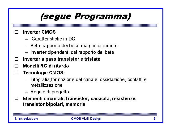
(segue Programma) q Inverter CMOS – Caratteristiche in DC – Beta, rapporto dei beta, margini di rumore – Inverter dipendenti dal rapporto dei beta q Inverter a pass transistor e tristate q Modelli RC di ritardo q Tecnologie CMOS: – Litografia, formazione del canale, ossidazione, contatti e metallizzazione – Regole di progetto q Elementi circuitali: transistor, caoacità, resistenze, transistor bipolari, memorie 1: Introduction CMOS VLSI Design 5

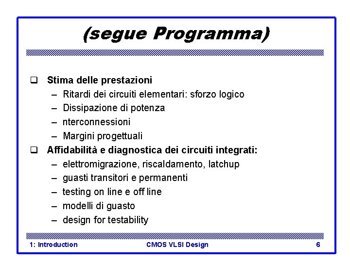
(segue Programma) q Stima delle prestazioni – Ritardi dei circuiti elementari: sforzo logico – Dissipazione di potenza – nterconnessioni – Margini progettuali q Affidabilità e diagnostica dei circuiti integrati: – elettromigrazione, riscaldamento, latchup – guasti transitori e permanenti – testing on line e off line – modelli di guasto – design for testability 1: Introduction CMOS VLSI Design 6

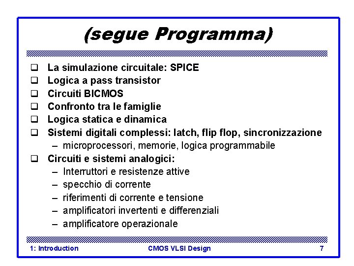
(segue Programma) q q q La simulazione circuitale: SPICE Logica a pass transistor Circuiti BICMOS Confronto tra le famiglie Logica statica e dinamica Sistemi digitali complessi: latch, flip flop, sincronizzazione – microprocessori, memorie, logica programmabile q Circuiti e sistemi analogici: – Interruttori e resistenze attive – specchio di corrente – riferimenti di corrente e tensione – amplificatori invertenti e differenziali – amplificatore operazionale 1: Introduction CMOS VLSI Design 7

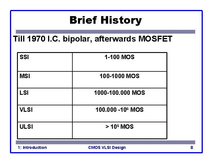
Brief History Till 1970 I. C. bipolar, afterwards MOSFET SSI 1 -100 MOS MSI 100 -1000 MOS LSI 1000 -100. 000 MOS VLSI 100. 000 -106 MOS ULSI > 106 MOS 1: Introduction CMOS VLSI Design 8

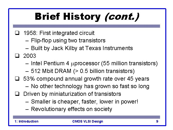
Brief History (cont. ) q 1958: First integrated circuit – Flip-flop using two transistors – Built by Jack Kilby at Texas Instruments q 2003 – Intel Pentium 4 mprocessor (55 million transistors) – 512 Mbit DRAM (> 0. 5 billion transistors) q 53% compound annual growth rate over 45 years – No other technology has grown so fast so long q Driven by miniaturization of transistors – Smaller is cheaper, faster, lower in power! – Revolutionary effects on society 1: Introduction CMOS VLSI Design 9

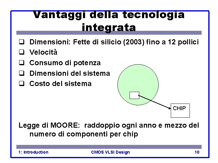
Vantaggi della tecnologia integrata q q q Dimensioni: Fette di silicio (2003) fino a 12 pollici Velocità Consumo di potenza Dimensioni del sistema Costo del sistema CHIP Legge di MOORE: raddoppio ogni anno e mezzo del numero di componenti per chip 1: Introduction CMOS VLSI Design 10

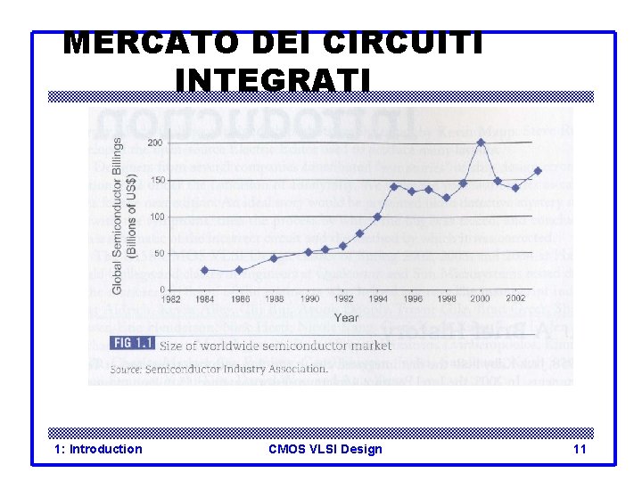
MERCATO DEI CIRCUITI INTEGRATI 1: Introduction CMOS VLSI Design 11

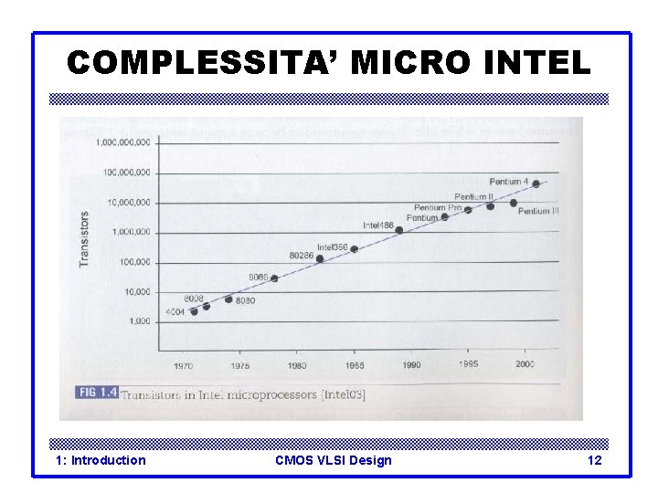
COMPLESSITA’ MICRO INTEL 1: Introduction CMOS VLSI Design 12

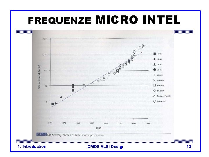
FREQUENZE 1: Introduction MICRO INTEL CMOS VLSI Design 13

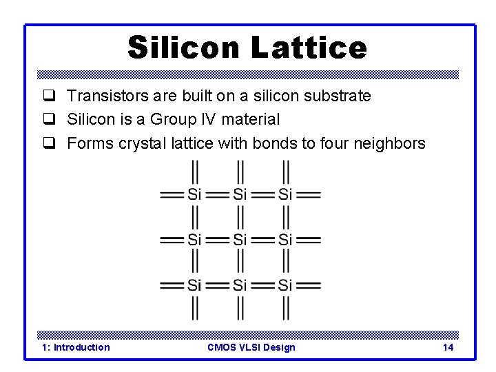
Silicon Lattice q Transistors are built on a silicon substrate q Silicon is a Group IV material q Forms crystal lattice with bonds to four neighbors 1: Introduction CMOS VLSI Design 14

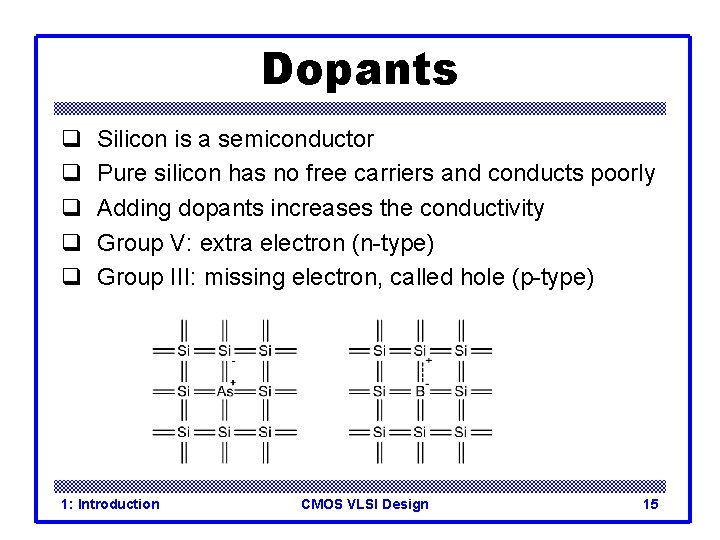
Dopants q q q Silicon is a semiconductor Pure silicon has no free carriers and conducts poorly Adding dopants increases the conductivity Group V: extra electron (n-type) Group III: missing electron, called hole (p-type) 1: Introduction CMOS VLSI Design 15

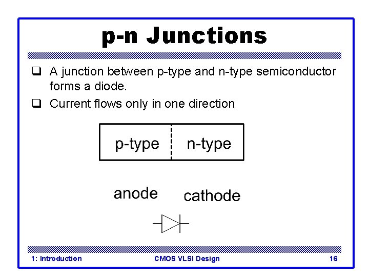
p-n Junctions q A junction between p-type and n-type semiconductor forms a diode. q Current flows only in one direction 1: Introduction CMOS VLSI Design 16

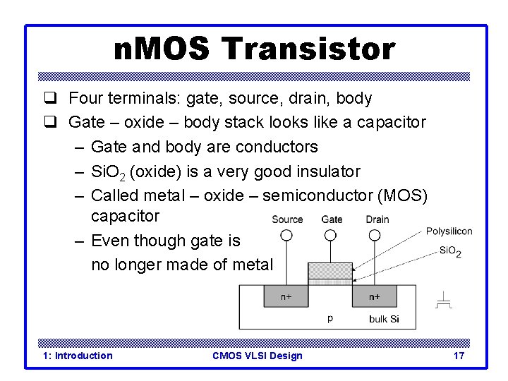
n. MOS Transistor q Four terminals: gate, source, drain, body q Gate – oxide – body stack looks like a capacitor – Gate and body are conductors – Si. O 2 (oxide) is a very good insulator – Called metal – oxide – semiconductor (MOS) capacitor – Even though gate is no longer made of metal 1: Introduction CMOS VLSI Design 17

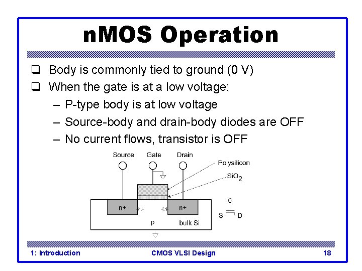
n. MOS Operation q Body is commonly tied to ground (0 V) q When the gate is at a low voltage: – P-type body is at low voltage – Source-body and drain-body diodes are OFF – No current flows, transistor is OFF 1: Introduction CMOS VLSI Design 18

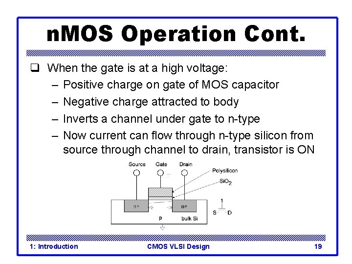
n. MOS Operation Cont. q When the gate is at a high voltage: – Positive charge on gate of MOS capacitor – Negative charge attracted to body – Inverts a channel under gate to n-type – Now current can flow through n-type silicon from source through channel to drain, transistor is ON 1: Introduction CMOS VLSI Design 19

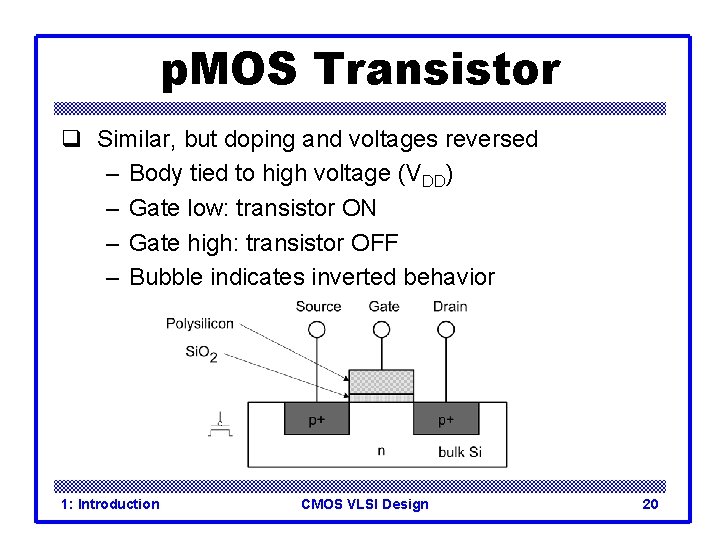
p. MOS Transistor q Similar, but doping and voltages reversed – Body tied to high voltage (VDD) – Gate low: transistor ON – Gate high: transistor OFF – Bubble indicates inverted behavior 1: Introduction CMOS VLSI Design 20

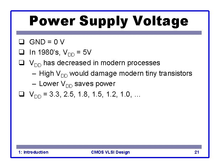
Power Supply Voltage q GND = 0 V q In 1980’s, VDD = 5 V q VDD has decreased in modern processes – High VDD would damage modern tiny transistors – Lower VDD saves power q VDD = 3. 3, 2. 5, 1. 8, 1. 5, 1. 2, 1. 0, … 1: Introduction CMOS VLSI Design 21

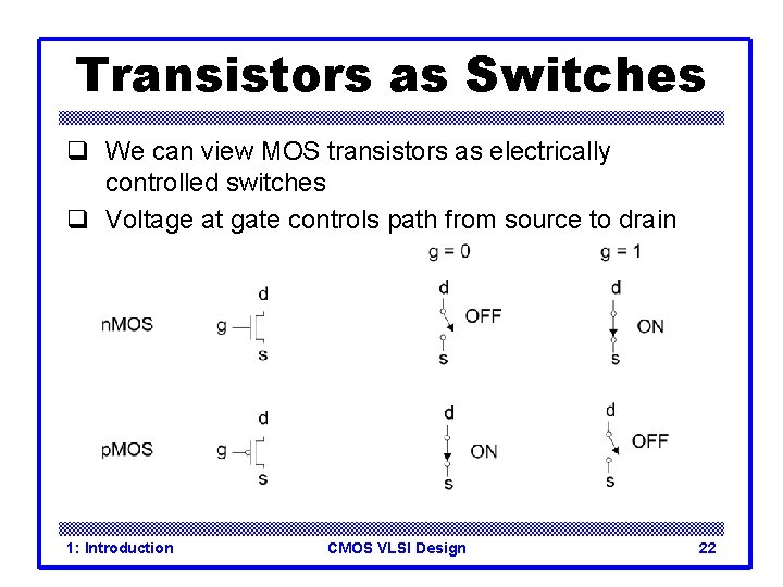
Transistors as Switches q We can view MOS transistors as electrically controlled switches q Voltage at gate controls path from source to drain 1: Introduction CMOS VLSI Design 22

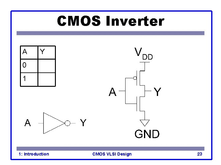
CMOS Inverter A Y 0 1 1: Introduction CMOS VLSI Design 23

CMOS Inverter A Y 0 1: Introduction CMOS VLSI Design 24

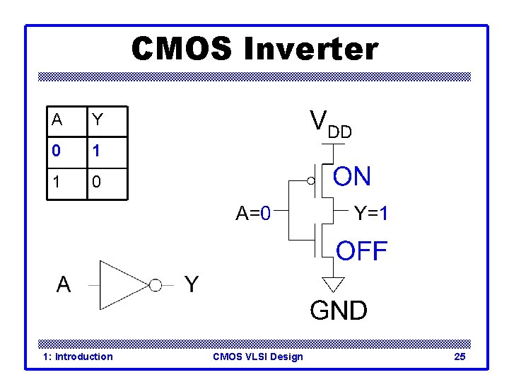
CMOS Inverter A Y 0 1 1 0 1: Introduction CMOS VLSI Design 25

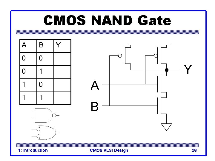
CMOS NAND Gate A B 0 0 0 1 1 1: Introduction Y CMOS VLSI Design 26

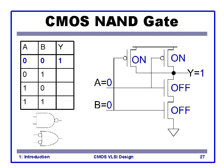
CMOS NAND Gate A B Y 0 0 1 1 1: Introduction CMOS VLSI Design 27

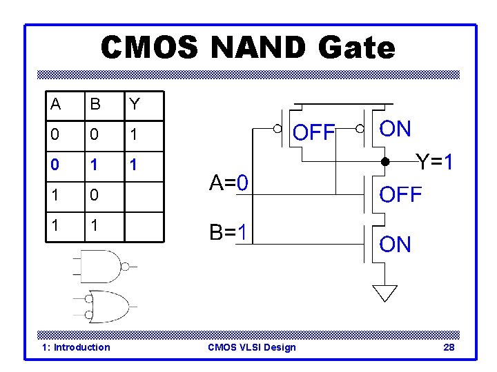
CMOS NAND Gate A B Y 0 0 1 1 1: Introduction CMOS VLSI Design 28

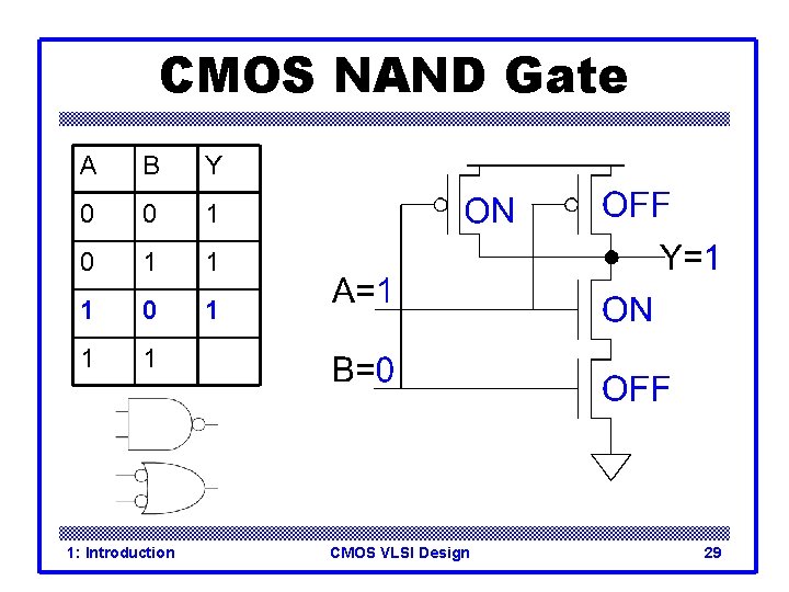
CMOS NAND Gate A B Y 0 0 1 1 1 0 1 1: Introduction CMOS VLSI Design 29

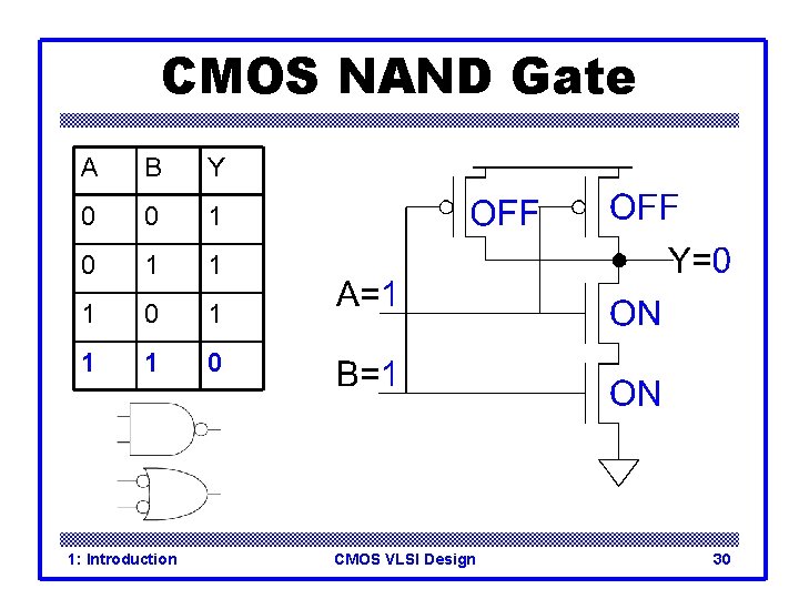
CMOS NAND Gate A B Y 0 0 1 1 1 0 1: Introduction CMOS VLSI Design 30

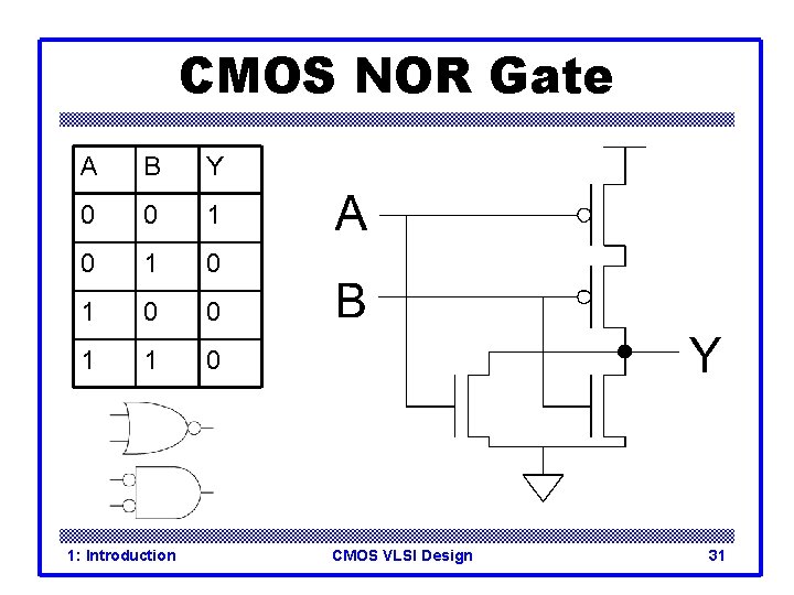
CMOS NOR Gate A B Y 0 0 1 0 1 0 0 1 1 0 1: Introduction CMOS VLSI Design 31

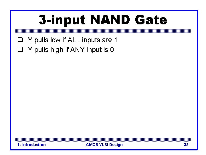
3 -input NAND Gate q Y pulls low if ALL inputs are 1 q Y pulls high if ANY input is 0 1: Introduction CMOS VLSI Design 32

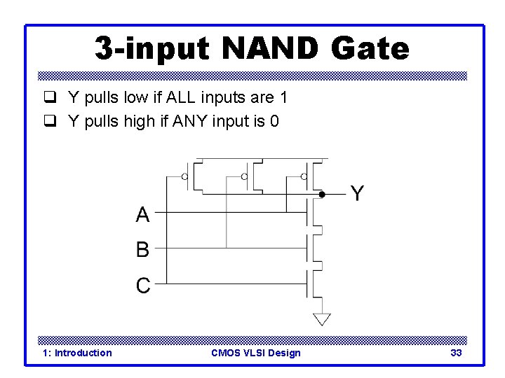
3 -input NAND Gate q Y pulls low if ALL inputs are 1 q Y pulls high if ANY input is 0 1: Introduction CMOS VLSI Design 33

CMOS Fabrication q CMOS transistors are fabricated on silicon wafer q Lithography process similar to printing press q On each step, different materials are deposited or etched q Easiest to understand by viewing both top and crosssection of wafer in a simplified manufacturing process 1: Introduction CMOS VLSI Design 34

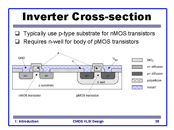
Inverter Cross-section q Typically use p-type substrate for n. MOS transistors q Requires n-well for body of p. MOS transistors 1: Introduction CMOS VLSI Design 35

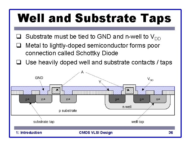
Well and Substrate Taps q Substrate must be tied to GND and n-well to VDD q Metal to lightly-doped semiconductor forms poor connection called Schottky Diode q Use heavily doped well and substrate contacts / taps 1: Introduction CMOS VLSI Design 36

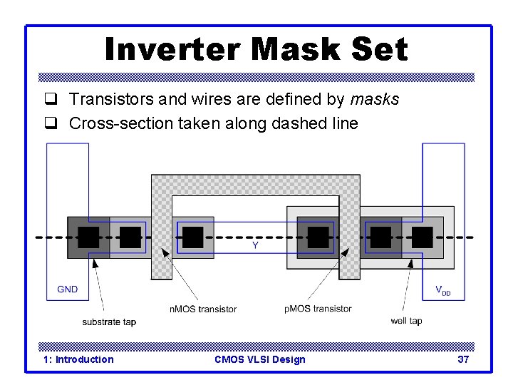
Inverter Mask Set q Transistors and wires are defined by masks q Cross-section taken along dashed line 1: Introduction CMOS VLSI Design 37

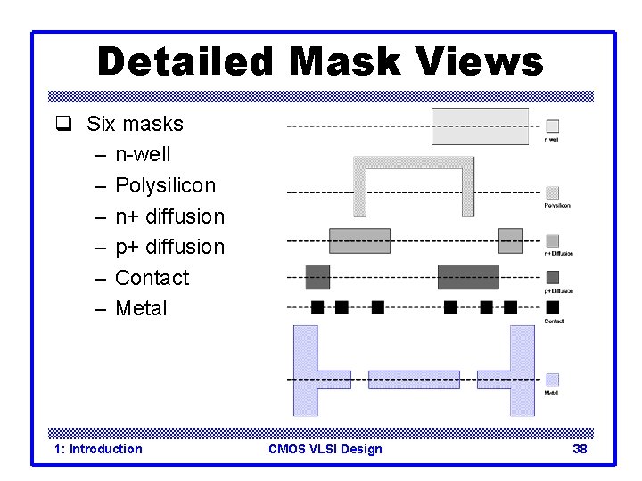
Detailed Mask Views q Six masks – n-well – Polysilicon – n+ diffusion – p+ diffusion – Contact – Metal 1: Introduction CMOS VLSI Design 38

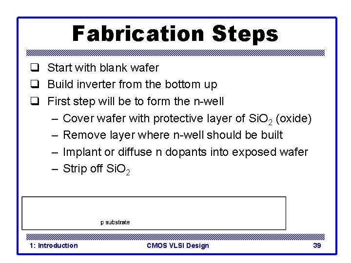
Fabrication Steps q Start with blank wafer q Build inverter from the bottom up q First step will be to form the n-well – Cover wafer with protective layer of Si. O 2 (oxide) – Remove layer where n-well should be built – Implant or diffuse n dopants into exposed wafer – Strip off Si. O 2 1: Introduction CMOS VLSI Design 39

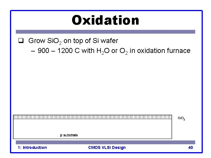
Oxidation q Grow Si. O 2 on top of Si wafer – 900 – 1200 C with H 2 O or O 2 in oxidation furnace 1: Introduction CMOS VLSI Design 40

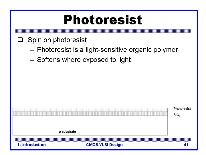
Photoresist q Spin on photoresist – Photoresist is a light-sensitive organic polymer – Softens where exposed to light 1: Introduction CMOS VLSI Design 41

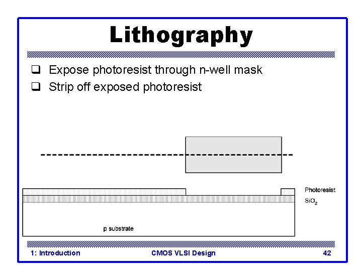
Lithography q Expose photoresist through n-well mask q Strip off exposed photoresist 1: Introduction CMOS VLSI Design 42

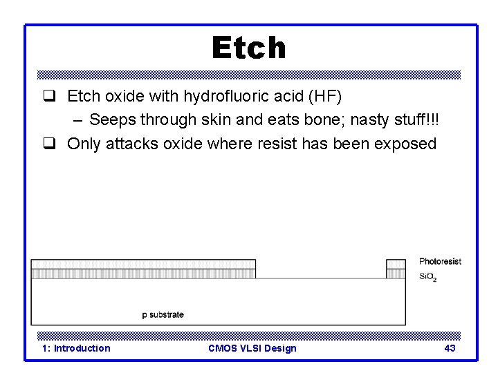
Etch q Etch oxide with hydrofluoric acid (HF) – Seeps through skin and eats bone; nasty stuff!!! q Only attacks oxide where resist has been exposed 1: Introduction CMOS VLSI Design 43

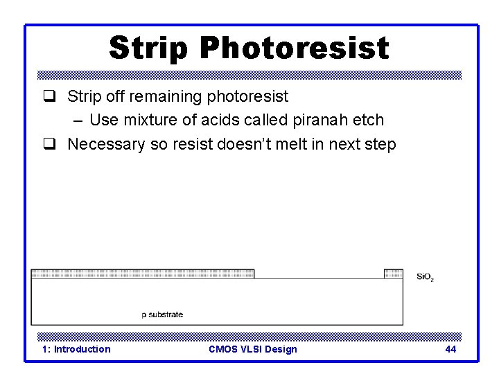
Strip Photoresist q Strip off remaining photoresist – Use mixture of acids called piranah etch q Necessary so resist doesn’t melt in next step 1: Introduction CMOS VLSI Design 44

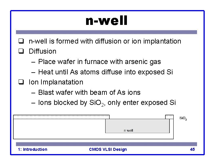
n-well q n-well is formed with diffusion or ion implantation q Diffusion – Place wafer in furnace with arsenic gas – Heat until As atoms diffuse into exposed Si q Ion Implanatation – Blast wafer with beam of As ions – Ions blocked by Si. O 2, only enter exposed Si 1: Introduction CMOS VLSI Design 45

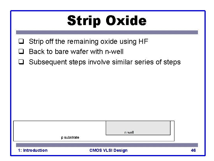
Strip Oxide q Strip off the remaining oxide using HF q Back to bare wafer with n-well q Subsequent steps involve similar series of steps 1: Introduction CMOS VLSI Design 46

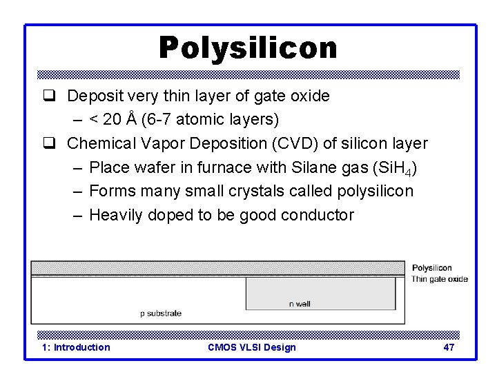
Polysilicon q Deposit very thin layer of gate oxide – < 20 Å (6 -7 atomic layers) q Chemical Vapor Deposition (CVD) of silicon layer – Place wafer in furnace with Silane gas (Si. H 4) – Forms many small crystals called polysilicon – Heavily doped to be good conductor 1: Introduction CMOS VLSI Design 47

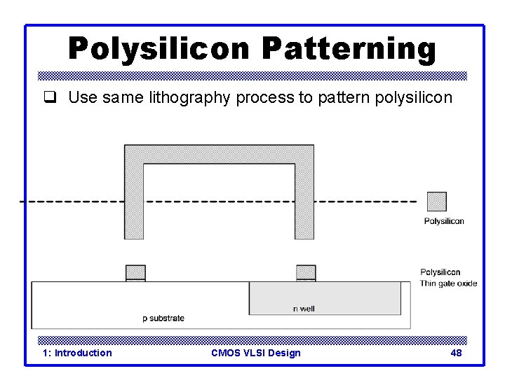
Polysilicon Patterning q Use same lithography process to pattern polysilicon 1: Introduction CMOS VLSI Design 48

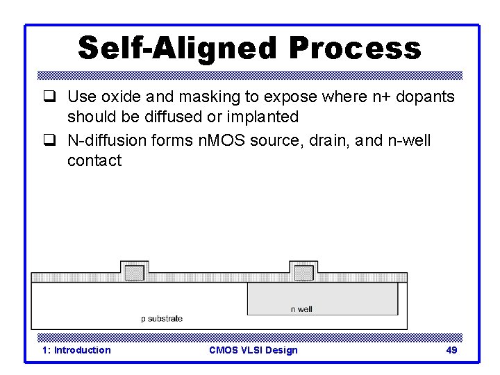
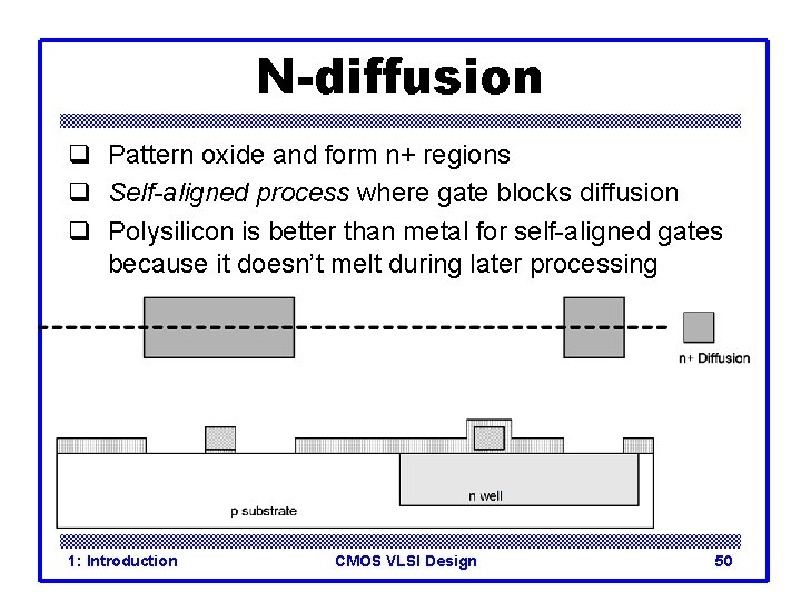
Self-Aligned Process q Use oxide and masking to expose where n+ dopants should be diffused or implanted q N-diffusion forms n. MOS source, drain, and n-well contact 1: Introduction CMOS VLSI Design 49

N-diffusion q Pattern oxide and form n+ regions q Self-aligned process where gate blocks diffusion q Polysilicon is better than metal for self-aligned gates because it doesn’t melt during later processing 1: Introduction CMOS VLSI Design 50

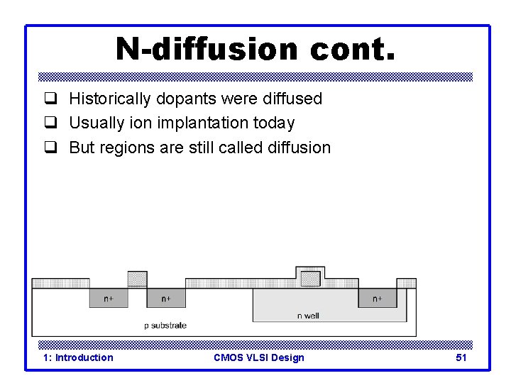
N-diffusion cont. q Historically dopants were diffused q Usually ion implantation today q But regions are still called diffusion 1: Introduction CMOS VLSI Design 51

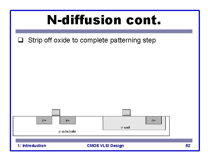
N-diffusion cont. q Strip off oxide to complete patterning step 1: Introduction CMOS VLSI Design 52

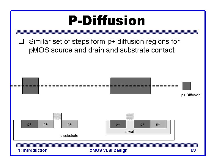
P-Diffusion q Similar set of steps form p+ diffusion regions for p. MOS source and drain and substrate contact 1: Introduction CMOS VLSI Design 53

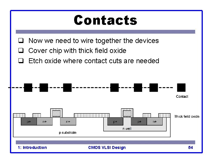
Contacts q Now we need to wire together the devices q Cover chip with thick field oxide q Etch oxide where contact cuts are needed 1: Introduction CMOS VLSI Design 54

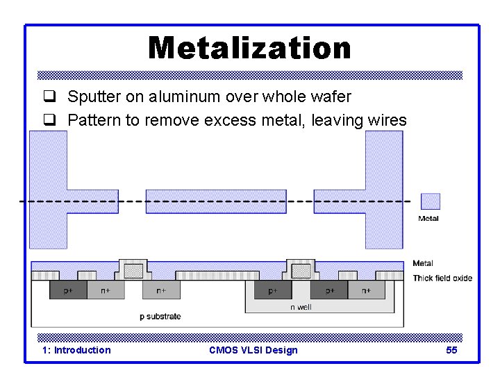
Metalization q Sputter on aluminum over whole wafer q Pattern to remove excess metal, leaving wires 1: Introduction CMOS VLSI Design 55

Layout q Chips are specified with set of masks q Minimum dimensions of masks determine transistor size (and hence speed, cost, and power) q Feature size f = distance between source and drain – Set by minimum width of polysilicon q Feature size improves 30% every 3 years or so q Normalize for feature size when describing design rules q Express rules in terms of l = f/2 – E. g. l = 0. 3 mm in 0. 6 mm process 1: Introduction CMOS VLSI Design 56

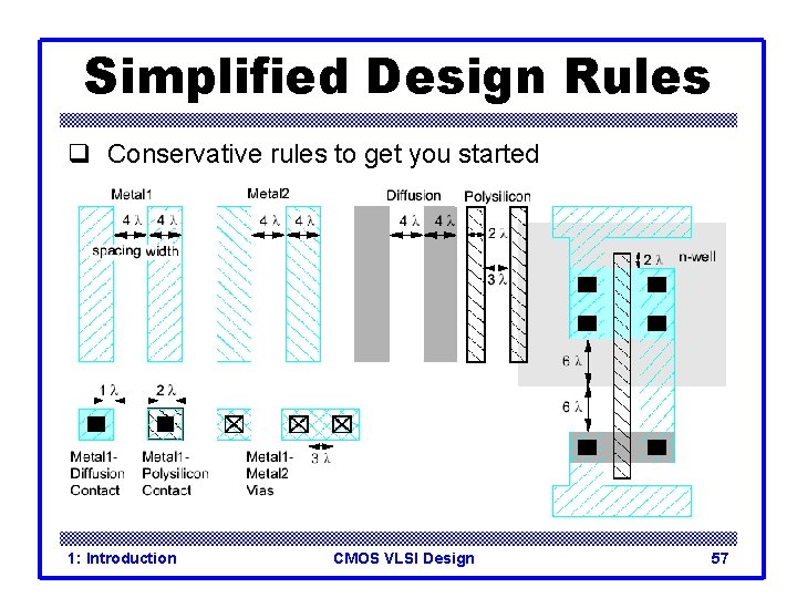
Simplified Design Rules q Conservative rules to get you started 1: Introduction CMOS VLSI Design 57

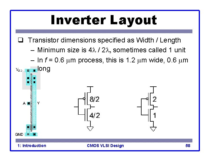
Inverter Layout q Transistor dimensions specified as Width / Length – Minimum size is 4 l / 2 l, sometimes called 1 unit – In f = 0. 6 mm process, this is 1. 2 mm wide, 0. 6 mm long 1: Introduction CMOS VLSI Design 58

Summary q q MOS Transistors are stack of gate, oxide, silicon Can be viewed as electrically controlled switches Build logic gates out of switches Draw masks to specify layout of transistors q Now you know everything necessary to start designing schematics and layout for a simple chip! 1: Introduction CMOS VLSI Design 59