LowPower and HighSpeed Interconnect Using Serial Passive Compensation

- Slides: 31

Low-Power and High-Speed Interconnect Using Serial Passive Compensation Chun-Chen Liu and Chung-Kuan Cheng Computer Science and Engineering Dept. University of California, San Diego http: //www. cse. ucsd. edu/~kuan/

Outline l Motivation l Previous Works and Our Contributions l Proposed Passive Compensation Technique ¤ Theory ¤ Experiments: An MCM stripline Case l Analytical Performance Prediction l Experimental Results and Future Work

Motivation l Technology Advancement: Interconnect is one bottleneck of system performance. l Bandwidth Increase: Interchip communication is expected to exceed 15 GHz in 2010. l Low Power Requirement: IO consumes one major portion of chip power budget.

Previous Works Overview l On-chip serial link signaling schemes ¤ ¤ Pre-emphasis and equalization (W. Dally, ’ 98) Clocked discharging (Horowitz, ISVLSI’ 03) Frequency modulation (Wong, JSSC’ 03, Jose, ISVLSI‘ 05) Non-linear transmission line (Hajimiri, JSSC’ 05, E. C. Kan, CICC’ 05) l Passive compensation ¤ ¤ Resistive termination (Hashimoto, EPEP’ 04, Tsuchiya, CICC’ 04, Flynn, ICCAD’ 05, CICC’ 05) Surfliner (C. K Cheng, ASPDAC’ 07)

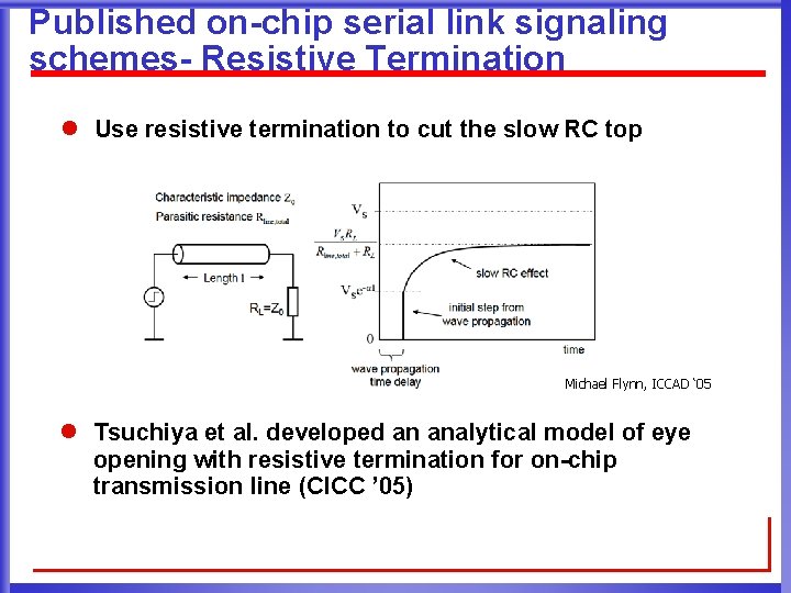
Published on-chip serial link signaling schemes- Resistive Termination l Use resistive termination to cut the slow RC top Michael Flynn, ICCAD ‘ 05 l Tsuchiya et al. developed an analytical model of eye opening with resistive termination for on-chip transmission line (CICC ’ 05)

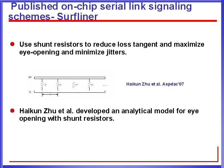
Published on-chip serial link signaling schemes- Surfliner l Use shunt resistors to reduce loss tangent and maximize eye-opening and minimize jitters. Haikun Zhu et al. Aspdac’ 07 l Haikun Zhu et al. developed an analytical model for eye opening with shunt resistors.

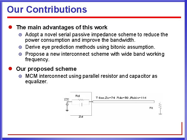
Our Contributions l The main advantages of this work ¤ ¤ ¤ Adopt a novel serial passive impedance scheme to reduce the power consumption and improve the bandwidth. Derive eye prediction methods using bitonic assumption. Propose a new interconnect scheme with wide band working frequency. l Our proposed scheme ¤ MCM interconnect using parallel resistor and capacitor as equalizer.

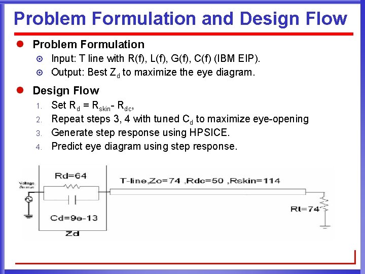
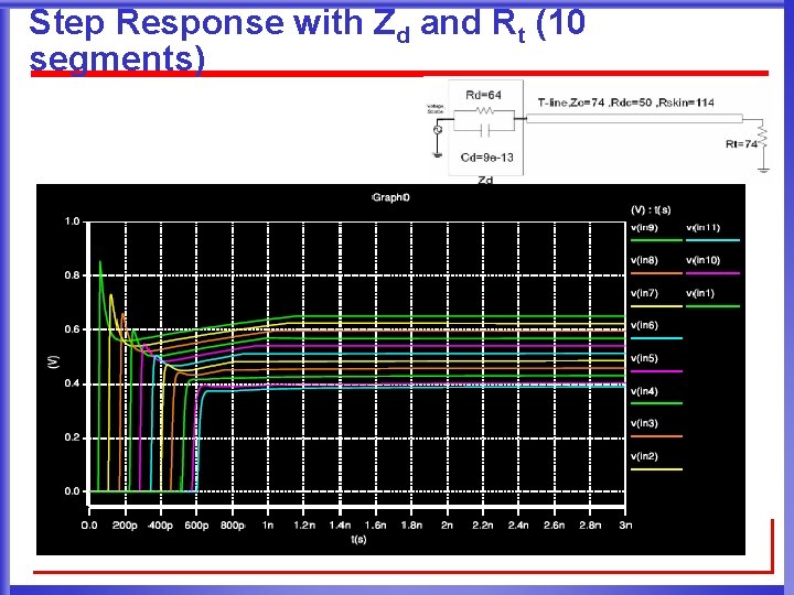
Problem Formulation and Design Flow l Problem Formulation ¤ ¤ Input: T line with R(f), L(f), G(f), C(f) (IBM EIP). Output: Best Zd to maximize the eye diagram. l Design Flow 1. 2. 3. 4. Set Rd = Rskin- Rdc, Repeat steps 3, 4 with tuned Cd to maximize eye-opening Generate step response using HPSICE. Predict eye diagram using step response.

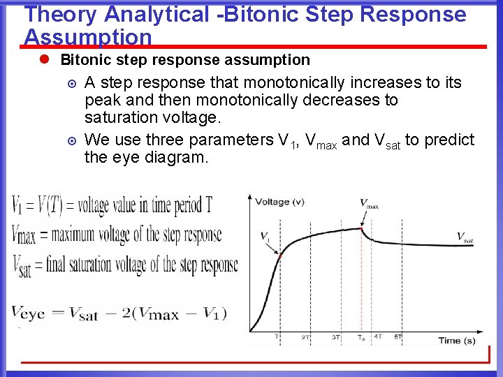
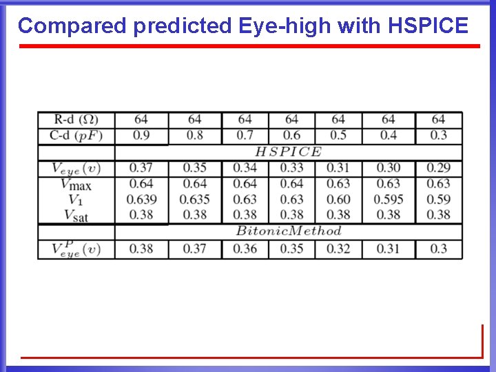
Theory Analytical -Bitonic Step Response Assumption l Bitonic step response assumption ¤ ¤ A step response that monotonically increases to its peak and then monotonically decreases to saturation voltage. We use three parameters V 1, Vmax and Vsat to predict the eye diagram.

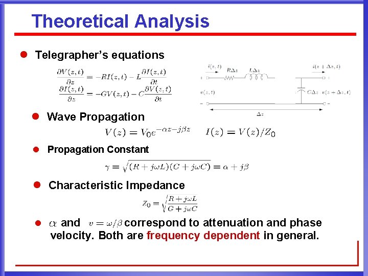
Theoretical Analysis l Telegrapher’s equations l Wave Propagation l Propagation Constant l Characteristic Impedance l and correspond to attenuation and phase velocity. Both are frequency dependent in general.

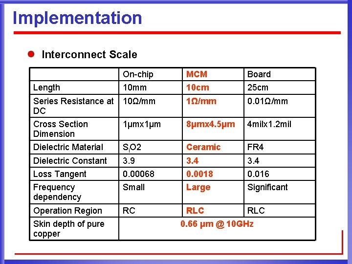
Implementation l Interconnect Scale On-chip MCM Board Length 10 mm 10 cm 25 cm Series Resistance at DC 10Ω/mm 1Ω/mm 0. 01Ω/mm Cross Section Dimension 1μmx 1μm 8μmx 4. 5μm 4 milx 1. 2 mil Dielectric Material Si. O 2 Ceramic FR 4 Dielectric Constant 3. 9 3. 4 Loss Tangent 0. 00068 0. 0018 0. 016 Frequency dependency Small Large Significant Operation Region RC RLC Skin depth of pure copper 0. 66 μm @ 10 GHz

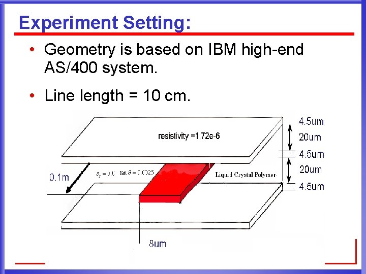
Experiment Setting: • Geometry is based on IBM high-end AS/400 system. • Line length = 10 cm.

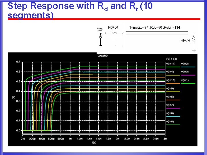
Step Response with Rd and Rt (10 segments)

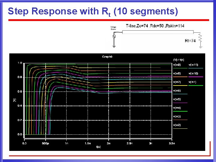
Step Response with Rt (10 segments)

Step Response with Zd and Rt (10 segments)

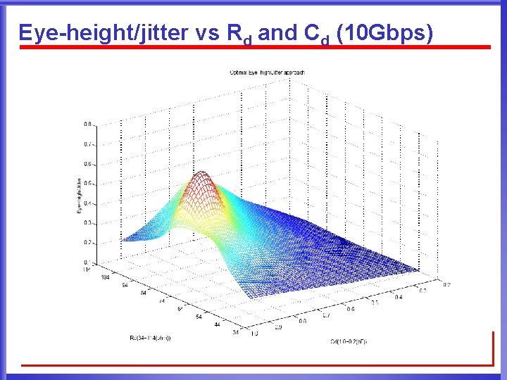
Eye-height/jitter vs Rd and Cd (10 Gbps)

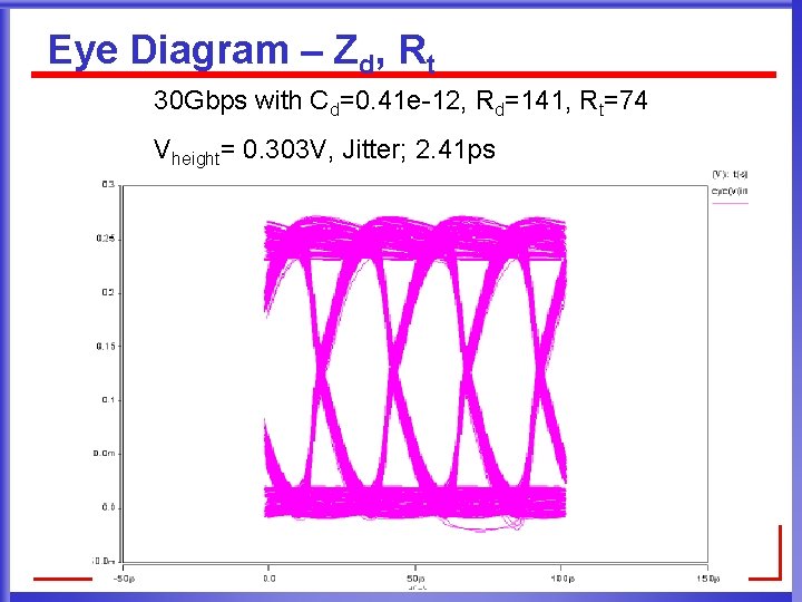
Eye Diagram – Zd, Rt 30 Gbps with Cd=0. 41 e-12, Rd=141, Rt=74 Vheight= 0. 303 V, Jitter; 2. 41 ps

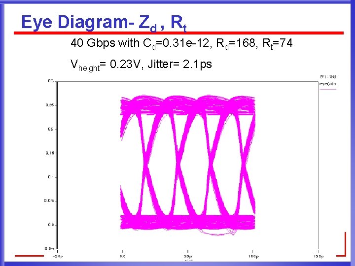
Eye Diagram- Zd , Rt 40 Gbps with Cd=0. 31 e-12, Rd=168, Rt=74 Vheight= 0. 23 V, Jitter= 2. 1 ps

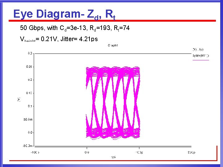
Eye Diagram- Zd, Rt 50 Gbps, with Cd=3 e-13, Rd=193, Rt=74 Vheight= 0. 21 V, Jitter= 4. 21 ps

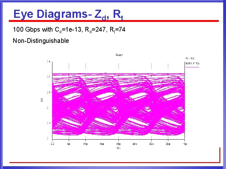
Eye Diagrams- Zd, Rt 100 Gbps with Cd=1 e-13, Rd=247, Rt=74 Non-Distinguishable

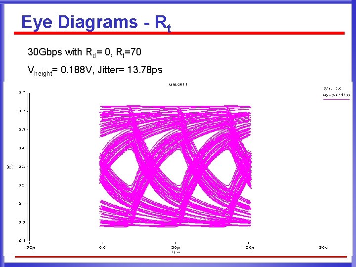
Eye Diagrams - Rt 30 Gbps with Rd= 0, Rt=70 Vheight= 0. 188 V, Jitter= 13. 78 ps

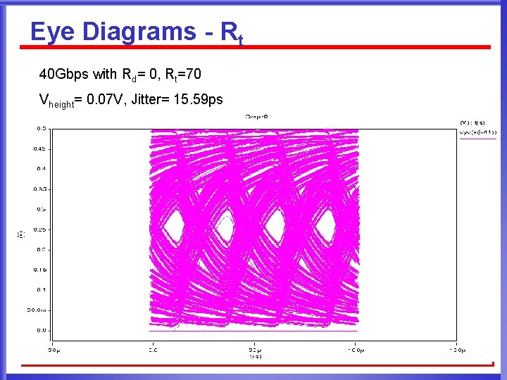
Eye Diagrams - Rt 40 Gbps with Rd= 0, Rt=70 Vheight= 0. 07 V, Jitter= 15. 59 ps

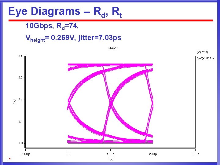
Eye Diagrams – Rd, Rt 10 Gbps, Rd=74, Vheight= 0. 269 V, jitter=7. 03 ps

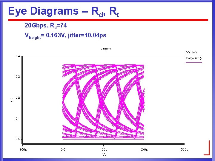
Eye Diagrams – Rd, Rt 20 Gbps, Rd=74 Vheight= 0. 163 V, jitter=10. 04 ps

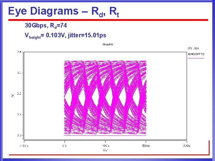
Eye Diagrams – Rd, Rt 30 Gbps, Rd=74 Vheight= 0. 103 V, jitter=15. 01 ps

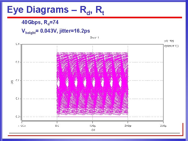
Eye Diagrams – Rd, Rt 40 Gbps, Rd=74 Vheight= 0. 043 V, jitter=16. 2 ps

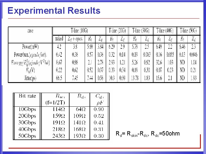
Experimental Results Rd= Rskin-Rdc, Rdc=50 ohm

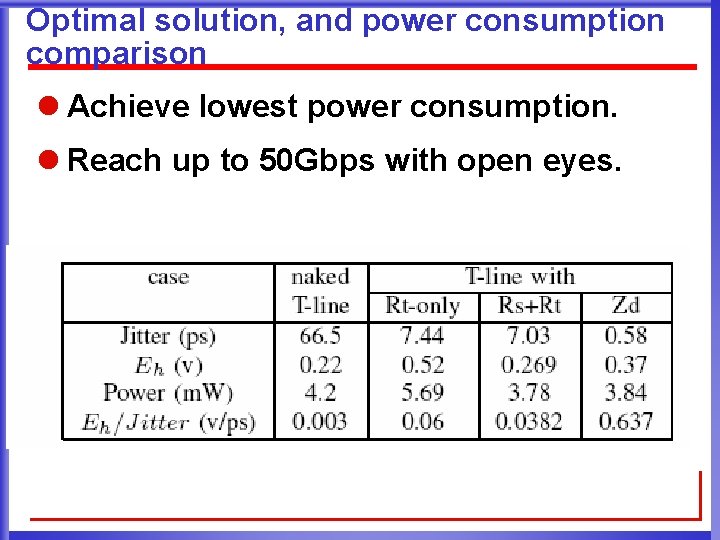
Optimal solution, and power consumption comparison l Achieve lowest power consumption. l Reach up to 50 Gbps with open eyes.

Compared predicted Eye-high with HSPICE

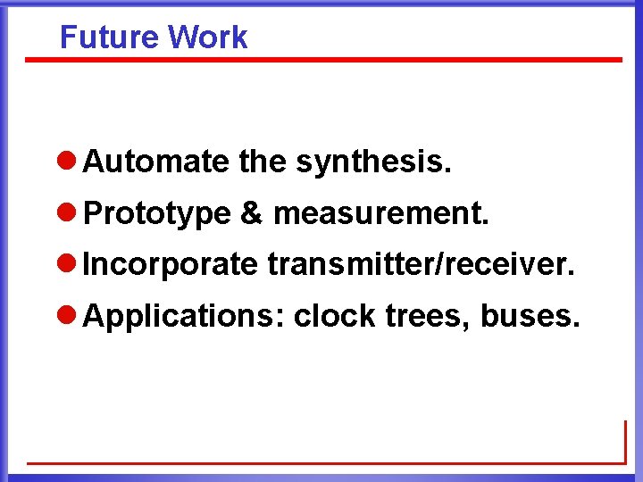
Future Work l Automate the synthesis. l Prototype & measurement. l Incorporate transmitter/receiver. l Applications: clock trees, buses.

Q/A Thank You