LOGIC FAMILIES UNIT IV ICs Logic gates and


")


")
- Slides: 27
LOGIC FAMILIES UNIT IV
ICs • Logic gates and memory devices are fabricated as IC s because components like resistors , diodes, BJTs …. . are an integral part of the chip • The various components are interconnected within the chip to form an e circuit during assembly • Advantages : increased reliability , reduced weight and size • SSI – fewer than 10 gates • MSI – 12 -100 gates/chip • LSI – 100 -5000 gates/chip • VLSI – several 1000 gates • Ics – Digital /Analog
LOGIC FAMILIES • Based on IC fabrication process – Bipolar and MOS • BIPOLAR: Elements – Resistors , Transistors and Diodes Can be saturated or non saturated SATURATED LOGIC: NON SATURATED LOGIC: 1. Resistor Transistor Logic 1. Schottky Logic 2. Direct Coupled Transistor Logic 2. Emitter – Coupled Logic 3. Diode Transistor Logic MOS FAMILIES 4. High Threshold Logic 1. PMOS – P Channel MOSFET 5. Transistor - Transistor Logic 2. NMOS – N Channel MOSFET 6. Integrated Injection Logic 3. CMOS – Complementary MOS
CHARACTERISTICS – DIGITAL ICS 1. 2. 3. 4. 5. 6. 7. Speed of Operation/Propagation Delay: The time taken for the output of the gate to change after the inputs have been changed Power Dissipation: Measure of power consumed by the logic gate when fully driven by all its inputs and is expressed in m. W/n. W Fan In: No of inputs connected to the gate without any degradation in the voltage levels Fan Out Max no of similar logic gates that a gate can drive without any degradation in voltage levels Noise Immunity: Max noise voltage that may appear at the input of a logic gatewithout changing the logical state of its output The difference between the operating input logic voltage level and the threshold voltage – Noise Margin Operating requirements -sensitive to temperature - varies between commercial, military , industrial applications Power supply requirements
TRANSISTOR LOGIC -TTL Speed 1. Fastest switching speed compared to others 2. Basic circuit – TTL logic family – NAND gate 3. Uses a special single multi emitter transistor that is fabricated with several emitters at its input– instead of diode – small area –yield increases- lower capacitance to the substrate – reduces circuit rise and fall time – high speed 4. No of emitters depends on fan in
TRANSISTOR LOGIC -TTL
TRANSISTOR LOGIC -TTL • Output from collector of transistor Q 4 • Each emitter of Q 1 acts as diode • Q 1 + 4 kohm - 3 input and gate-rest of the circuit acts like inverter • Overall circuit – 3 input nand gate • When a/b/c – are at 0 v (logic 0 ) –the corresponding EB junction Q 1 F/W biased • Rb selected such that Q 1 is turned on • Ib 2 to base Q 2 reduced potential of base of Q 2 • Q 2 and Q 4 -cut off • Output voltage Vcc - Logic 1
TRANSISTOR LOGIC -TTL • If all the inputs are high – logic 1 – EB of Q 1 R/B Biased - No base current • Q 1 off – CB F/W biased supplying Ib 2 to Q 2 - Saturates Q 2 -Q 2 on –Drop across R 2 F/W biases BE juction of Q 4 -Q 4 on • Output of the collector is low – Logic 0 • The function of D – Prevents Q 3 and Q 4 simultaneously on • In the absence of diode Q 3 conducts slightly- Output low • To prevent D between Q 3 E and Q 4 C • Volt drop across diode keeps BE jn of Q 3 RB • Q 4 conducts when output is low- NAND operation
TTL Gate with Totem-Pole Output(NAND)
EMITTER COUPLED LOGIC -ECL
EMITTER COUPLED LOGIC -ECL 1. Current mode logic 2. Non saturated digital logic family 3. Operates the transistors in active mode-Eliminates turn off/saturation delay – Faster switching speed among all bipolar devices 4. Propagation delay – 1 ns 5. Large Silicon area- Dissipates high power 6. Basic circuit – Differential amplifier 7. VEE – Fixed current IE 8. Depending upon Vin (Logic 1 - -0. 8 V or Logic 0 - -1. 7 V) Current switches between collectors of Q 1 and Q 2 9. Vc 1 and Vc 2 complements each other- Output voltage not equal to input logic levels 10. Made equal by emitter follower stages Q 3 and Q 4
ECL – NOR/OR GATE 1. Basic ECL – Inverter – Output at Vout 1 2. By connecting transistors in parallel with Q 1 , the basic circuit can be expanded to more than one input 3. A, B Input s low – Q and Q 1 both off – Q 2 on – active region – Output collector at low state – A+B – collector of Q 3 – A+B “ 4. A or B high – Q or Q 1 on - Q 2 off – collector at high state – A+B – Collector of Q 3 – A +B Complement
ECL NOR/OR GATE
CMOS FAMILIES 1. MOS – MOS structure – Metal electrode on an oxide insulator over a semi conductor substrate 2. PMOS – P channel enhancement MOSFET NMOS – N channel enhancement MOSFET CMOS – Both p and n channel devices
CMOS FAMILIES A B Y Q 1/Q 2 Q 3/Q 4 0 0 1 ON OFF 0 1 0 Q 1 Q 3 1 0 0 Q 2 Q 4 1 1 0 OFF ON N Channel MOS P Channel MOS
CMOS NOR GATE 1. Q 1 and Q 2 – PMOS transistors 2. Q 3 and Q 4 – NMOS transistors 3. A and B low – Both PMOS ON – Both NMOS OFF Output – Vdd – HIGH 4. A or B high – associated PMOS OFF – associated NMOS ON – Output Low 5. CMOS OR – CMOS NOR+CMOS inverter
CMOS FAMILIES A B Y Q 1/Q 4 Q 3/Q 2 0 0 1 ON OFF 0 1 1 Q 3 1 0 1 Q 4 Q 2 1 1 0 OFF ON
CMOS NAND GATE 1. Q 1 and Q 4 – PMOS transistors in parallel 2. Q 2 and Q 3 – NMOS transistors in series 3. A and B high – Both PMOS OFF – Both NMOS ON Output – Vdd – low 4. A or B low – associated PMOS On – associated NMOS Off – Output High 5. CMOS AND – CMOS NAND +CMOS inverter
CMOS INVERTER 1. 2. 3. 4. 5. 6. 7. 8. Q 2 – driver , Q 2 OFF –NMOS – Q 1 – load , PMOS – Drains connected together – Output Source and substrate connected together Gates to common input Source of Q 1 – VDD Source of Q 2 grounded Vin low – Q 2 OFF –Q 1 ON - Output high Vin High – Vice Versa - INVERTER
CMOS INVERTER
• CPLD PAL and GAL are available only in small sizes, equivalent to a few hundred logic gates. For bigger logic circuits, complex PLD (CPLD) can be used. These contain the equivalent of several PAL linked by programmable interconnections, all in one integrated circuit. CPLDs can replace thousands, or even hundreds of thousands, of logic gates. • FPGA uses a grid of logic gates, similar to that of an ordinary gate array, but the programming of connection is done by the customer, not by the manufacturer.
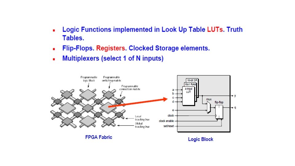
FPGA Ø Field Programmable Gate Array ØMonolithic highly integrated circuits –VLSI ØCustom- SEMI CUSTOM – Programmable logic ØIC designed to be configured by a customer or a designer after manufacturing ØModern day technology for building a breadboard or prototype from standard parts ØProgrammable logic blocks and programmable interconnects allow the same FPGA to be used in many different applications ØFPGA contain an array of programmable logic blocks and a hierarchy of reconfigurable interconnects that allows the blocks to be wired together like many logic gates that can be inter wired in different configurations ØFPGA configuration is generally specified using a HARDWARE DESCRIPTION LANGUAGE (HDL) similar to Application Specific Integrated Circuit (ASIC)rate 6/9/2021 22
FPGA • Logic Blocks configured to perform combinational function. In most FPGAs logic blocks also include memory elements(FF) or complete blocks of memory • CLB – Configurable Logic Blocks –fundamental building block of FPGA technology • Contemporary FPGAs have large resources of logic gates and RAM blocks to implement complex digital computations. 6/9/2021 23
FPGA • FPGA s member of class of devices called FPL, defined as programmable devices containing repeated fields of small logic blocks and elements(Configurable Logic Blocks(CLB) by Xilinx & Logic cell/Logic element LC/LE by Altera) Altera v. Gate arrays typically consist of a sea of NAND gates whose functions are customer provided in a wire list v. Wire list is used during the fabrication process to achieve the distinct definition of the final metal layer v. The designer of a programmable gate array solution has full control over the actual design implementation without the need and delay for any physical IC fabrication facility 6/9/2021 24
FPGA - ARCHITECTURE LOGIC BLOCKS Programmable Interconnect Routing channels Programmable Peripheral Devices
FPGA (Field Programmable Gate Array)