LOGIC CIRCUITS INTRODUCTION Aircraft logic systems follow the


 gates will only produce a logic")


 the nose landing gear door is open. §")


 devices provide us with a means of generating precise")


 have two clocked inputs (J and K),")


 - is the minimum value of high")
- Slides: 52
LOGIC CIRCUITS
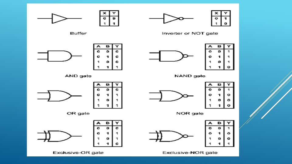
INTRODUCTION § Aircraft logic systems follow the same conventions and standards as those used in other electronic applications. § In particular, the MIL/ANSI standard logic symbols are invariably used and the logic elements they represent operate in exactly the same way as those used in non-aircraft applications. § MIL/ANSI standard symbols for the most common logic gates are shown together with their truth tables in Figure 5. 1. Buffers : Buffers do not affect the logical state of a digital signal (i. e. a logic 1 input results in a logic 1 output, whereas a logic 0 input results in a logic 0 output). Buffers are normally used to provide extra current drive at the output but can also be used to regularize the logic levels present at an interface.
INTRODUCTION Inverters : Inverters are used to complement the logical state (i. e. a logic 1 input results in a logic 0 output and vice versa). Inverters also provide extra current drive and, like buffers, are used in interfacing applications where they provide a means of regularizing logic levels present at the input or output of a digital system. AND gates : AND gates will only produce a logic 1 output when all inputs are simultaneously at logic 1. Any other input combination results in a logic 0 output. OR gates : OR gates will produce a logic 1 output whenever any one, or more, inputs are at logic 1. Putting this another way, an OR gate will only produce a logic 0 output whenever all of its inputs are simultaneously at logic 0. NAND gates : NAND (i. e. NOT-AND) gates will only produce a logic 0 output when all inputs are simultaneously at logic 1. Any other input combination will produce a logic 1 output. A NAND gate therefore is nothing more than an AND gate with its output inverted. The circle shown at the output of the gate denotes this inversion.
INTRODUCTION NOR gates : NOR (i. e. NOT-OR) gates will only produce a logic 1 output when all inputs are simultaneously at logic 0. Any other input combination will produce a logic 0 output. A NOR gate, therefore, is simply an OR gate with its output inverted. A circle is again used to indicate inversion. Exclusive-OR gates : Exclusive-OR gates will produce a logic 1 output whenever either one of the two inputs is at logic 1 and the other is at logic 0. Exclusive-OR gates produce a logic 0 output whenever both inputs have the same logical state (i. e. when both are at logic 0 or both are at logic 1). Exclusive-NOR gates : Exclusive-NOR gates will produce a logic 0 output whenever either one of the two inputs is at logic 1 and the other is at logic 0. Exclusive-OR gates produce a logic 1 output whenever both inputs have the same logical state (i. e. when both are at logic 0 or both are at logic 1).
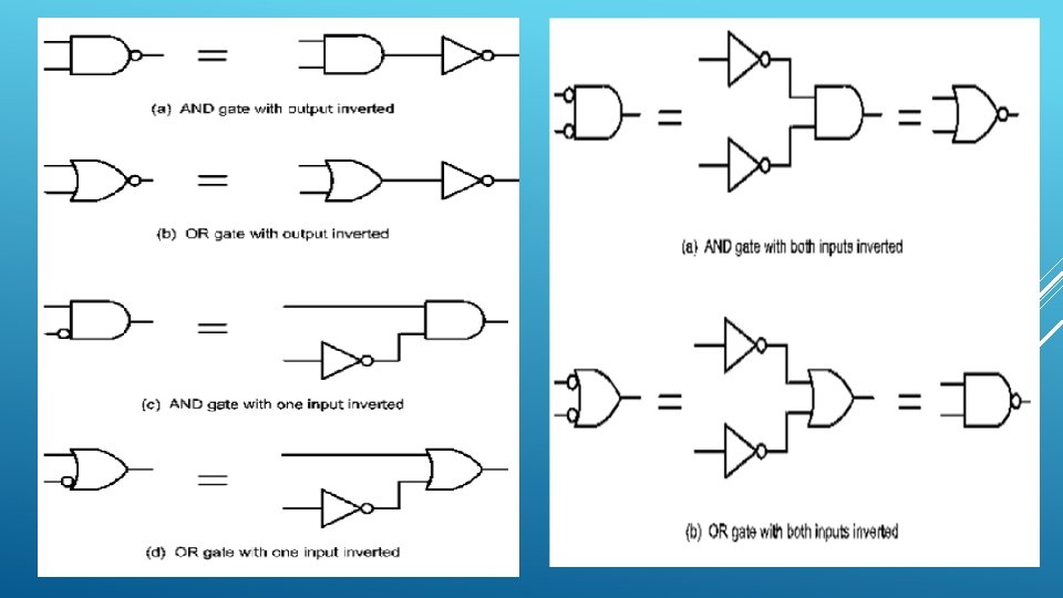
INTRODUCTION Inverted outputs and inputs : § The NAND and NOR gates that we have just met are said to have inverted outputs. § In other words, they are respectively equivalent to AND and OR gates with their outputs passed through an inverter (or NOT gate), as shown in Fig. § As well as inverted outputs, aircraft logic systems also tend to show logic gates in which one or more of the inputs are inverted. § In Figure 5. 2 c an AND gate is shown with one input inverted. This is equivalent to an inverter (NOT gate) connected to one input of the AND gate, as shown. § In Figure 5. 2 d an OR gate is shown with one input inverted. This is equivalent to an inverter (NOT gate) connected to one input of the OR gate, as shown. § Two further circuits with inverted inputs are shown in Figure 5. 3. In Figure 5. 3 a, both inputs of an AND gate are shown inverted. § This arrangement is equivalent to the two-input NOR gate shown. In Figure 5. 3 b, both inputs of an OR gate are shown inverted. This arrangement is equivalent to the two input NAND gate shown.
INTRODUCTION BOOLEAN ALGEBRA : Boolean algebra is frequently used to describe logical operations used in avionic systems. The rules (or laws) of Boolean algebra are as follows. The Commutative Law A + B = B + A A • B = B • A A + (B + C ) = ( A + B ) + C A • ( B • C ) = ( A • B ) • C The Distributive Law A • ( B + C ) = ( A • B ) + ( A • C ) The AND rules A • 0 = 0 A • 1 = A A • A’ = 0
INTRODUCTION The OR rules A + 0 = A A + 1 = 1 A + A’ = 1 A + A = A The NOT rules 0 = 1 1 = 0 A’’ = A (double inversion)
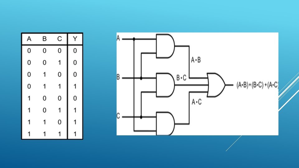
COMBINATIONAL LOGIC § By using a standard range of logic levels (i. e. voltage levels used to represent the logic 1 and logic 0 states) logic circuits can be combined together in order to solve more complex logic functions. § As an example, assume that a logic circuit is to be constructed that will produce a logic 1 output whenever two, or more, of its three inputs are at logic 1. § This circuit is referred to as a majority vote circuit and its truth table is shown in Fig below. § It shows the logic circuitry required and the Boolean expressions for the logic at each node in the circuit.
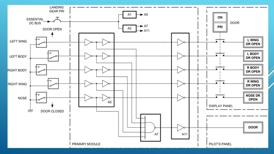
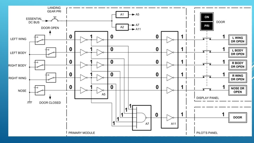
COMBINATIONAL LOGIC § Look at a more practical example of the use of logic in the typical aircraft system shown in Figure. § The inputs to this logic system consist of five switches that detect whether or not the respective landing gear door is open. § The output from the logic system is used to drive six warning indicators. Four of these are located on the overhead display panel and show which door (or doors) are left open, while an indicator located on the pilot’s instrument panel provides a master landing gear door warning. § A switch is also provided in order to enable or disable the five door warning indicators. § The landing gear warning logic primary module consists of the following integrated circuit devices: A 1 Regulated power supply for A 5 A 2 Regulated power supply for A 7 and A 11
COMBINATIONAL LOGIC A 1 Regulated power supply for A 5 A 2 Regulated power supply for A 7 and A 11 A 5 Ten inverting (NOT) gates A 7 Five-input NAND gates A 11 Six inverting (NOT) gates § Note that the power supply for A 1 and A 2 is derived from the essential services DC bus. § This is a 28 V DC bus which is maintained in the event of an aircraft generator failure. § Note also that the indicators are active-low devices (in other words, in Figure they require a logic 0 input in order to become illuminated).
COMBINATIONAL LOGIC § In order to understand how the landing gear warning logic works it is simply a matter of tracing logic 0 and logic 1 states through the logic diagram. § Figure below shows how this is done when all of the landing gear doors are closed (this is the normal in-flight condition). § Note how the primary door warning indicator shows the pilot that the system is active. § When all of the landing gear doors are closed all inputs to A 5 are taken to logic 0, all outputs from A 5 are at logic 0, as is the output from A 7. § This, in turn, results in logic 1 inputs to the indicators, which remain in the off (non illuminated) state.
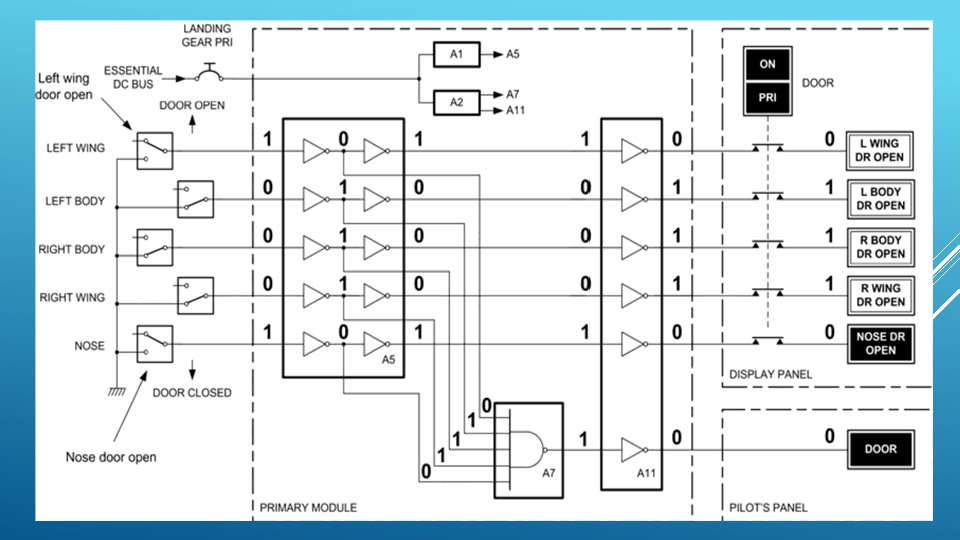
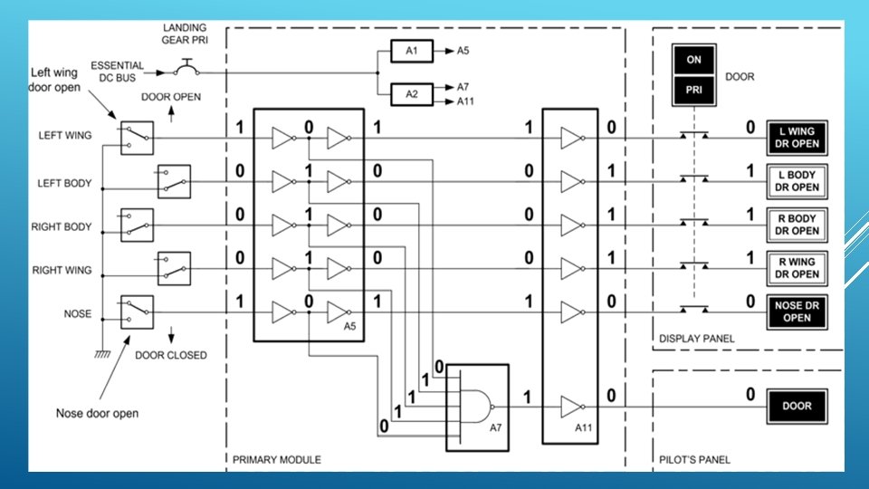
COMBINATIONAL LOGIC § In Figure (a) the nose landing gear door is open. § In this condition the output of A 7 goes to logic 1 and the master warning becomes illuminated on the pilot’s panel. § At the same time, the nose-door open warning becomes illuminated. § In Figure (b) both the left wing and the nose landing gear doors are open. § In this condition the output of A 7 goes to logic 1 and the master warning becomes illuminated as before. § This time, however, both the nose-door open and left-wing-door-open warnings become illuminated. § Note that in a real passenger aircraft a secondary landing gear door warning logic system is fitted. § This system is identical to the primary system shown and provides a back-up in case the primary system fails. Primary or secondary system operation can be selected by the pilot.
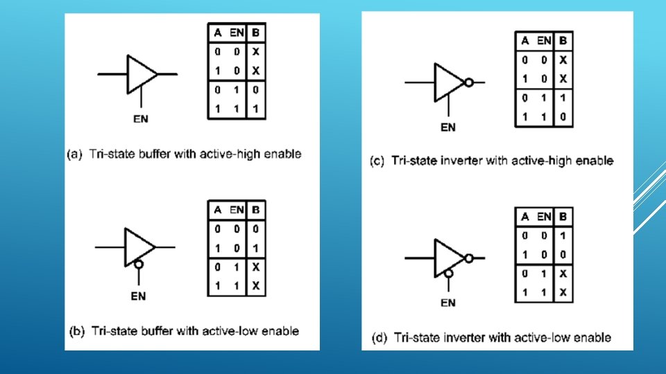
TRI-STATE LOGIC § Tristate logic devices operate in a similar manner to conventional logic gates but have a third, high impedance output state. § This high-impedance state permits the output of several tristate devices to be connected directly together. § Such arrangements are commonly used when a bus system has to be driven by several logic gates. § The output state (whether a logic level or high impedance) is controlled by means of an enable (EN) input. § This EN input may be either active-high or active- low, as shown in Figure. § Figures show the truth tables for a buffer with active-high and active-low enable inputs, respectively. § Note that the state of the EN input determines whether the output takes the same logical state as the input or whether the output is taken to its high impedance state (shown as X in the truth table).
TRI-STATE LOGIC § Figures show the truth table for an inverter with active-high and active-low enable inputs, respectively. § In this case, the state of the EN input determines whether the output takes the opposite logical state to the input or whether the output is taken to its highimpedance state (again shown as X in the truth table).
MONOSTABLES § Monostable (or one-shot) devices provide us with a means of generating precise time delays. § Such delays become important in many sequential logic applications where logic states are not constant but subject to change with time. § The action of a Monostable is quite simple – its output is initially logic 0 until a change of state occurs at its trigger input. § The level change can be from 0 to 1 (positive edge trigger) or 1 to 0 (negative edge trigger). § Immediately the trigger pulse arrives, the output of the Monostable changes state to logic 1. § It then remains at logic 1 for a pre-determined period before reverting back to logic 0. § Monostable circuits can be used as pulse stretchers (a means of elongating a short pulse) as well as producing accurate time delays.
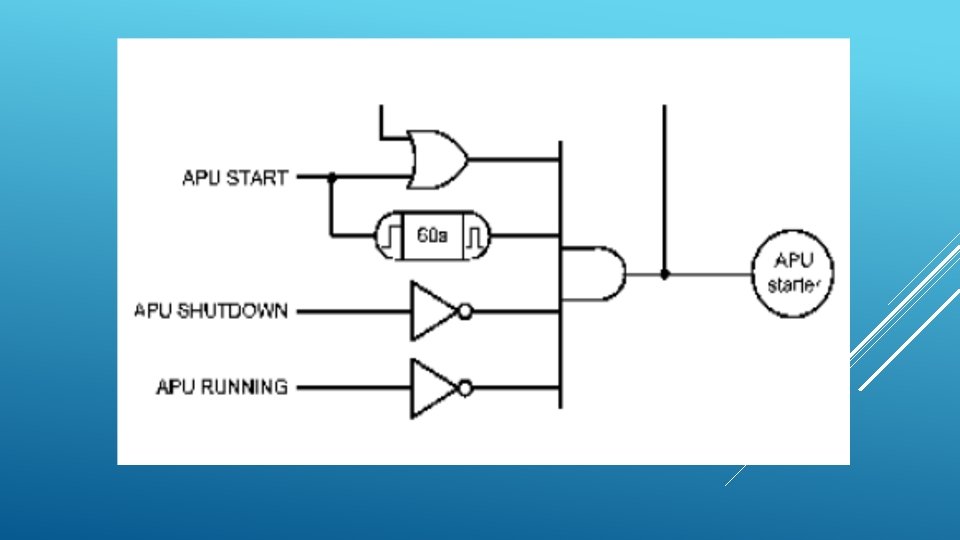
MONOSTABLES § An example of the use of a Monostable is shown in the auxiliary power unit (APU) starter logic shown in Figure. § This arrangement has three inputs (APU START, APU SHUTDOWN and APU RUNNING) and one output (APU STARTER MOTOR). § The inputs are all active-high (in other words, a logic 1 is generated when the pilot operates the APU START switch, and so on). § The output of the APU starter motor control logic goes to logic 1 in order to apply power to the starter motor via a large relay. § There a few things to note about the logic arrangement shown in Figure: 1. When the APU runs on its own we need to disengage the starter motor. In this condition the APU MOTOR signal needs to become inactive (i. e. it needs to revert to logic 0).
MONOSTABLES 2. We need to avoid the situation that might occur if the APU does not start but the starter motor runs continuously (as this will drain the aircraft batteries). Instead, we should run the starter motor for a reasonable time (say, 60 seconds) before disengaging the starter motor. The 60 seconds timing is provided by means of a positive edge triggered Monostable device. This device is triggered from the APU START signal. 3. Since the pilot is only required to momentarily press the APU START switch, we need to hold the condition until such time as the engine starts or times out (i. e. at the end of the 60 -second period). We can achieve this by OR-ing the momentary APU START signal with the APU STARTER MOTOR signal. 4. We need to provide a signal that the pilot can use to shutdown the APU (for example, when the aircraft’s main engines are running or perhaps in the event of a fault condition).
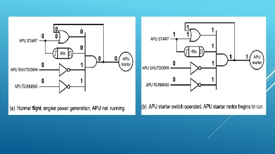
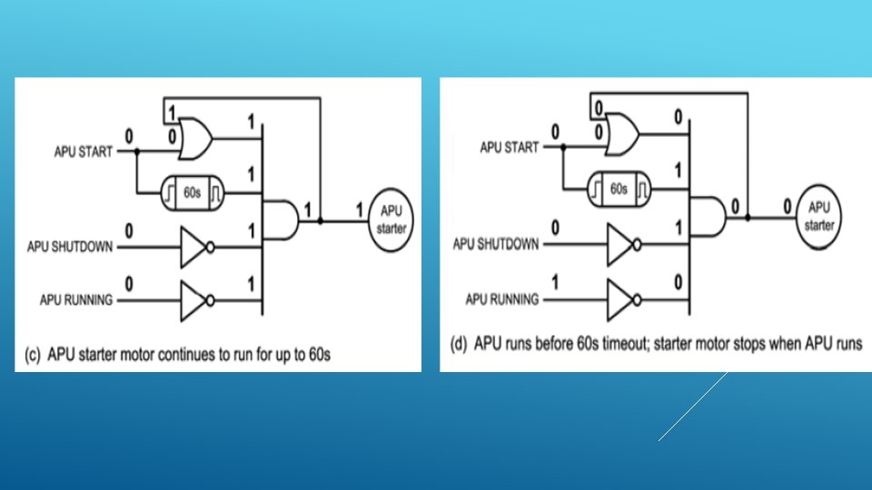
MONOSTABLES § In order to understand the operation of the APU starter motor logic system we can once again trace through the logic system using 1 s and 0 s to represent the logical condition at each point (just as we did for the landing gear door warning logic). § In Figure a the APU is in normal flight and the APU is not running. In this condition the main engines are providing the aircraft’s electrical power. § In Figure b the pilot is operating the APU START switch. § The monostable is triggered and output of the OR and AND gates both go to logic 1 in order to assert the APU STARTER MOTOR signal. § In Figure c the APU START signal is removed but the output of the AND gate is held at logic 1 by feeding back its logical state via the OR gate. § The monostable remains triggered and continues to produce a logic 1 output for its 60 -second period
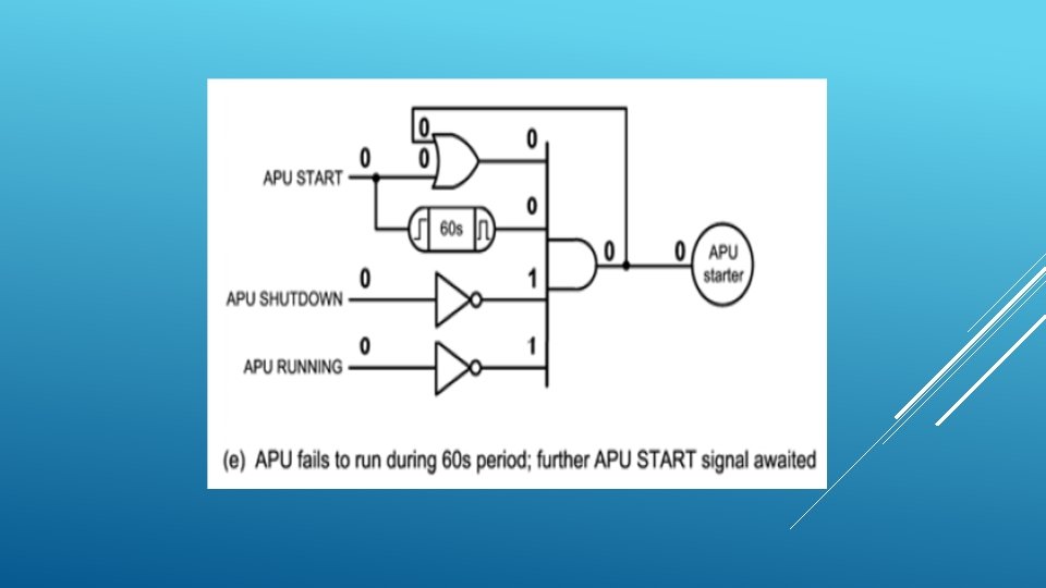
MONOSTABLES § In Figure d the APU is now running and the APU RUNNING signal has gone to logic 1 in order to signal this condition. § This results in the output of the AND gate going to logic 0 and the APU STARTER MOTOR signal is no longer made active. § The starter motor is therefore disengaged. § In Figure e the APU has failed to run during the 60 -second monostable period. In this timed-out condition the output of the AND gate goes to logic 0 and the APU STARTER MOTOR signal becomes inactive. § The system then waits for the pilot to operate the APU START button for a further attempt at starting!
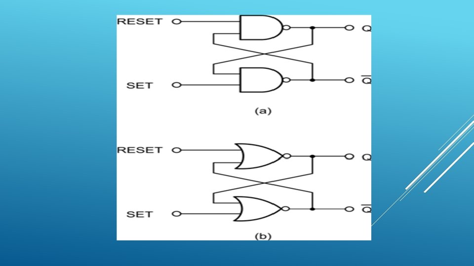
BISTABLES § The output of a bistable circuit has two stable states (logic 0 or logic 1). § Once set in one or other of these states, the output of a bistable will remain at a particular logic level for an indefinite period until reset. § A bistable thus forms a simple form of memory as it remains in its latched state (either set or reset) until a signal is applied to it in order to change its state (or until the supply is disconnected). § The simplest form of bistable is the R-S bistable. § This device has two inputs, SET and RESET, and complementary outputs, Q and Q. A logic 1 applied to the SET input will cause the Q output to become (or remain at) logic 1, while a logic 1 applied to the RESET input will cause the Q output to become (or remain at) logic 0. § In either case, the bistable will remain in its SET or RESET state until an input is applied in such a sense as to change the state. § Two simple forms of R-S bistable based on cross-coupled logic gates are shown in Figure.
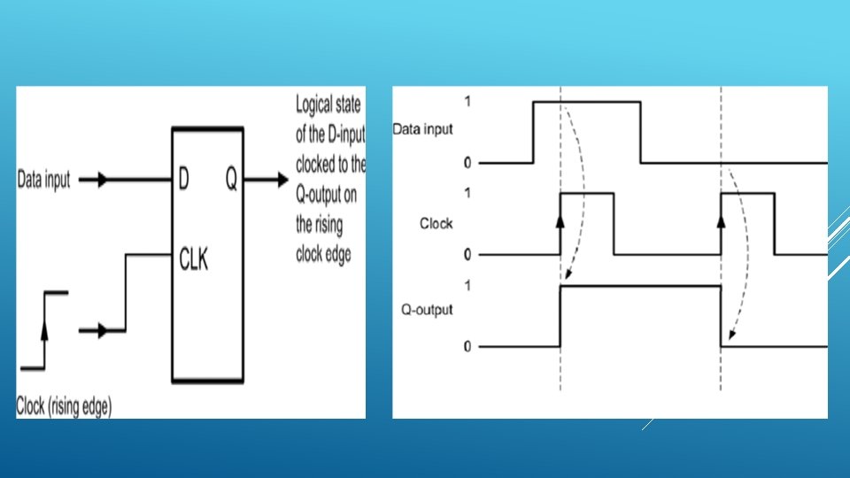
BISTABLES § The simple cross-coupled logic gate bistable has a number of serious shortcomings (consider what would happen if a logic 1 was simultaneously present on both the SET and RESET inputs!) and practical forms of bistable make use of much improved purposedesigned logic circuits such as D-type and J-K bistables. § The D-type bistable has two inputs: D (standing variously for ‘data’ or ‘delay’) and CLOCK (CLK). § The data input (logic 0 or logic 1) is clocked into the bistable such that the output state only changes when the clock changes state. § Operation is thus said to be synchronous. Additional subsidiary inputs (which are invariably active-low) are provided which can be used to directly set or reset the bistable. § These are usually called PRESET (PR) and CLEAR (CLR). D-type bistables are used both as latches (a simple form of memory) and as binary dividers. § The simple circuit arrangement in Figure together with the timing diagram which illustrate the operation of D-type bistables
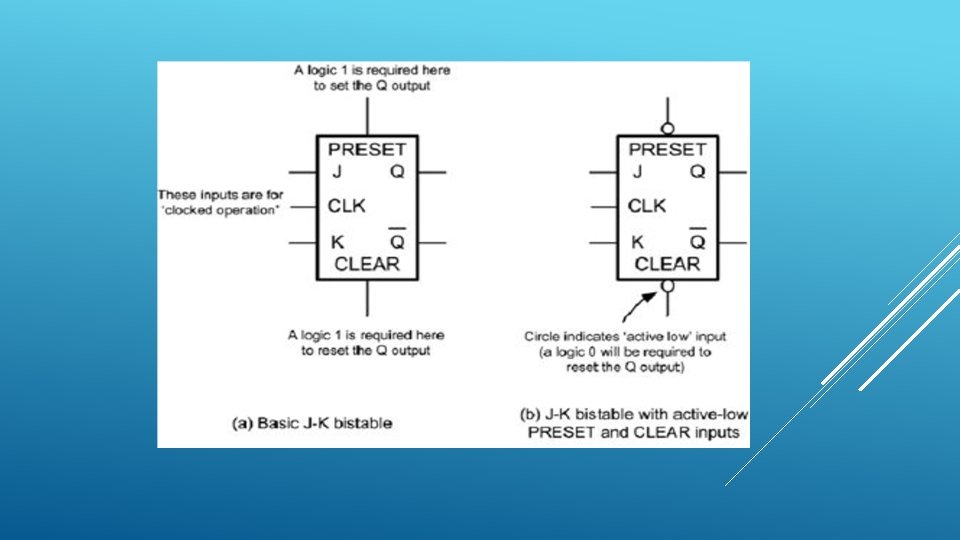
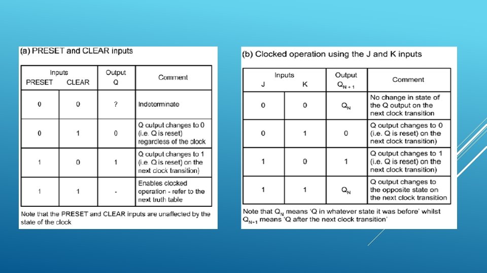
BISTABLES § J-K bistables (see Fig. ) have two clocked inputs (J and K), two direct inputs (PRESET and CLEAR), a CLOCK (CLK) input, and outputs (Q and Q]). § As with R-S bistables, the two outputs are complementary (i. e. when one is 0 the other is 1, and vice versa). § Similarly, the PRESET and CLEAR inputs are invariably both active-low (i. e. a 0 on the PRESET input will set the Q output to 1 whereas a 0 on the CLEAR input will set the Q output to 0). § Figure summarises the input and corresponding output states of a J-K bistable for various input states. § J-K bistables are the most sophisticated and flexible of the bistable types and they can be configured in various ways for use in binary dividers, shift registers and latches.
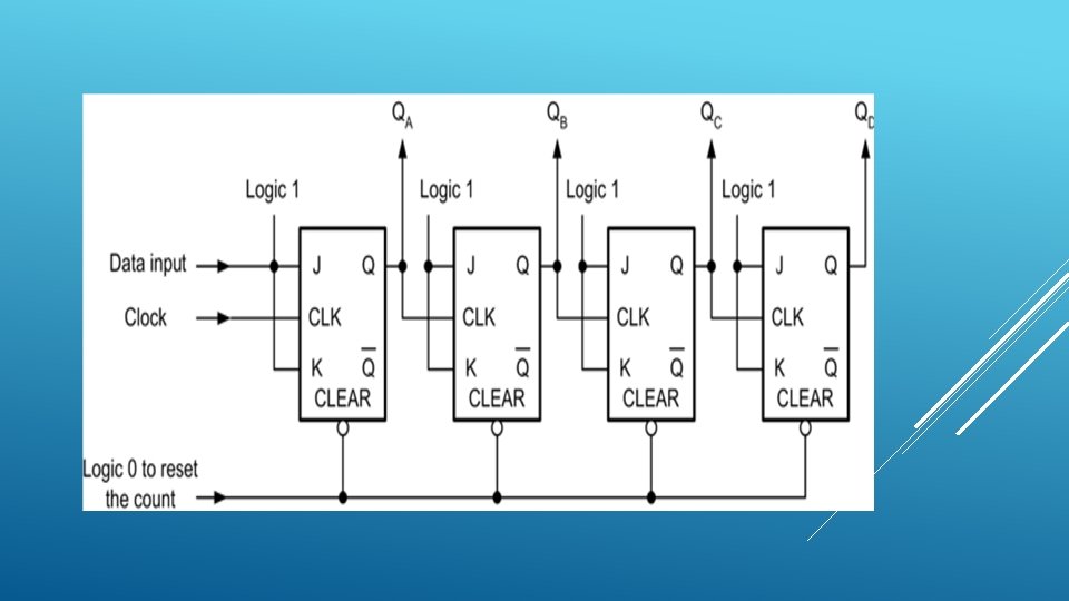
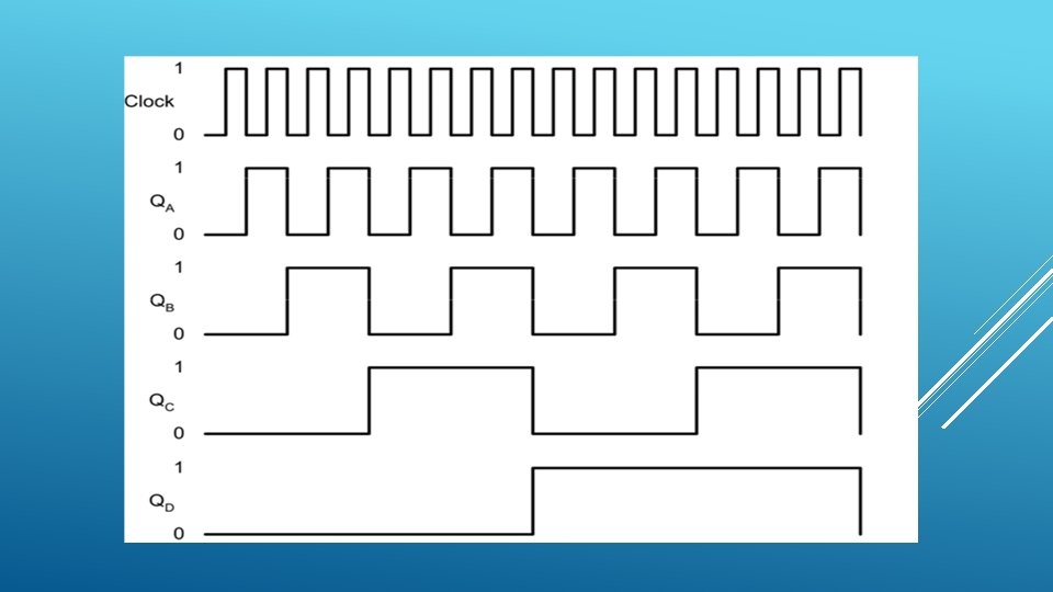
BINARY COUNTERS § Figure shows the arrangement of a four-stage binary counter based on J-K bistables. § The timing diagram for this circuit is shown in Figure. § § Each stage successively divides the clock input signal by a factor of two. Note that a logic 1 input is transferred to the respective Q-output on the falling edge of the clock pulse and all J and K inputs must be taken to logic 1 to enable binary counting.
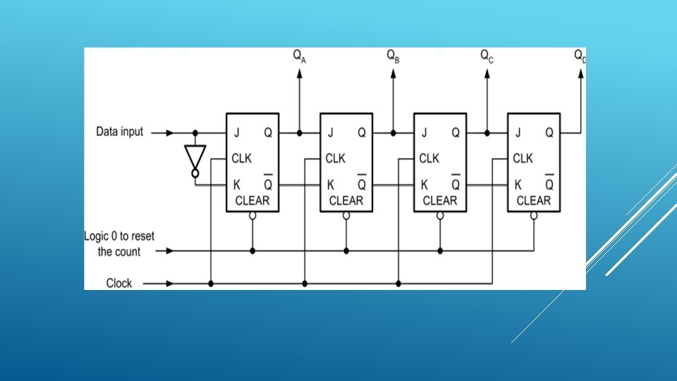
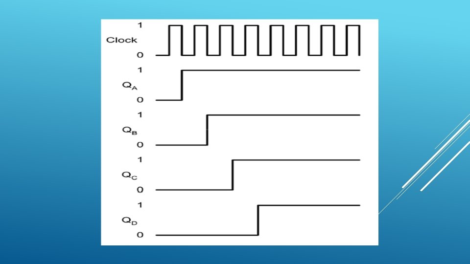
SHIFT REGISTERS § § § Figure shows the arrangement of a four-stage shift register based on J-K bistables. The timing diagram for this circuit is shown in Figure. Note that each stage successively feeds data (via the Q-output) to the next stage and that all data transfer occurs on the falling edge of the clock pulse.
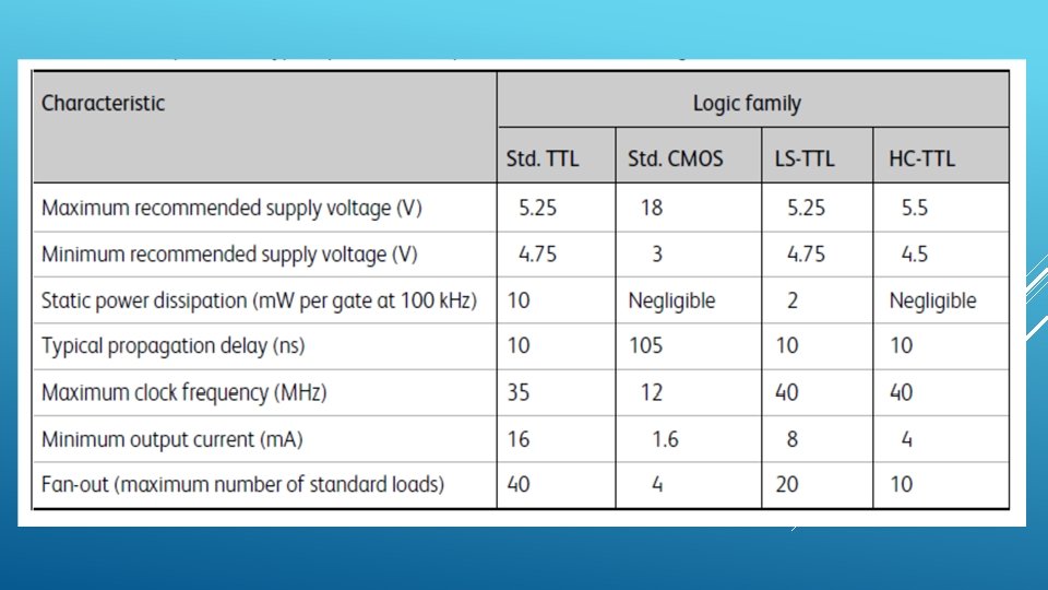
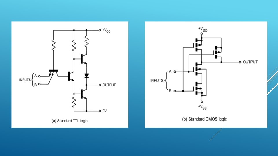
LOGIC FAMILIES The task of realizing a complex logic circuit is made simple with the aid of digital integrated circuits, which are classified according to the semiconductor technology used in their fabrication (the logic family to which a device belongs is largely instrumental in determining its operational characteristics, such as power consumption, speed and immunity to noise). The two basic logic families are complementary metal oxide semiconductor (CMOS) and transistor–transistor logic (TTL). Each of these families is then further sub-divided into classes that are based on refinements of the parent technology, such as ‘high-current’ (or buffered output), low-noise, etc. Representative circuits for a basic two-input NAND gate using TTL and CMOS technology are shown in Figures.
TTL LOGIC The most common family of TTL logic devices is the 74 -series. Devices from this family are coded with the prefix number 74 (e. g. 7400). Sub-families (based on the use of variations in the technology) are distinguished by letters which follow the initial prefix.
CMOS LOGIC The most common family of CMOS devices is the 4000 -series. Variants within the family are identified by the suffix letters :
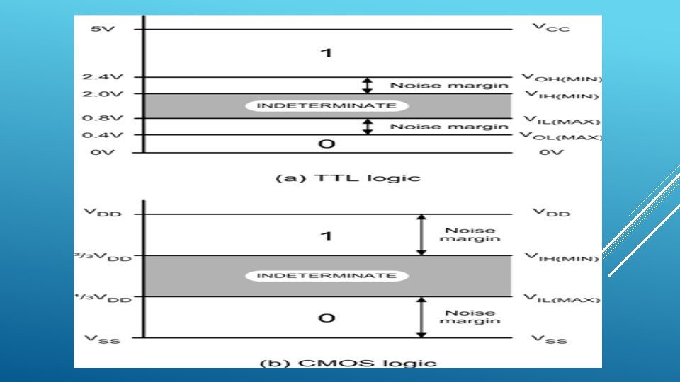
LOGIC LEVELS AND NOISE MARGIN
LOGIC LEVELS AND NOISE MARGIN Where VOH(MIN) - is the minimum value of high state (logic 1) output voltage, VIH(MIN)- is the minimum value of high state (logic 1) input voltage, VOL(MAX)- is the maximum value of low state (logic 0) output voltage VIL(MAX)- is the minimum value of low state (logic 0) input voltage. The noise margin for standard 7400 series TTL is typically 400 m. V, while that for CMOS is (1/3) VDD, as shown in Figure.