LightEmitting Diodes LED Lecturer Mauro Mosca www dieet
- Slides: 40

Light-Emitting Diodes (LED) Lecturer: Mauro Mosca (www. dieet. unipa. it/tfl) last release: 02/11/2020 University of Palermo – Master in Electronic Engineering

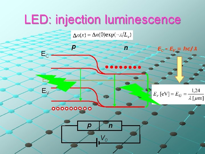
LED: injection luminescence EC p n EF EC - EV = hc/l EF EV p n V 0

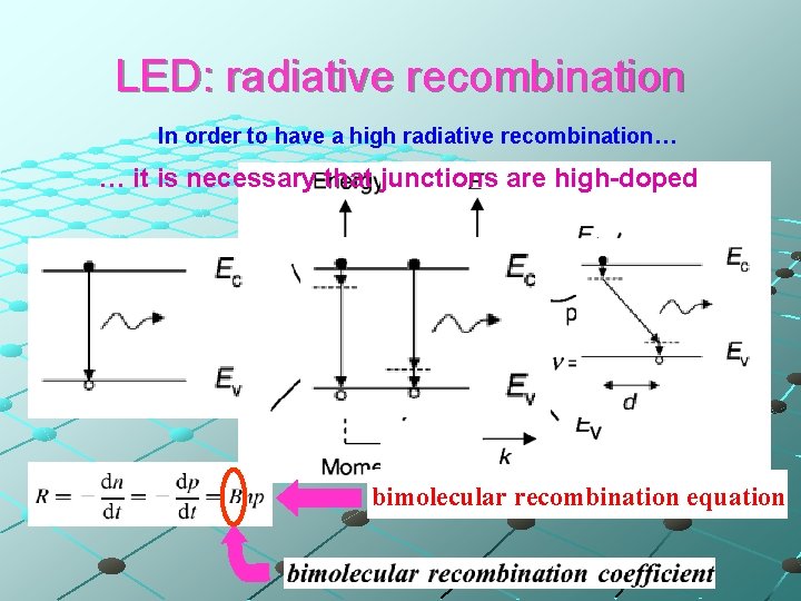
LED: radiative recombination In order to have a high radiative recombination… … it is necessary that junctions are high-doped bimolecular recombination equation

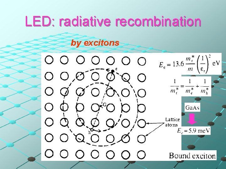
LED: radiative recombination by excitons

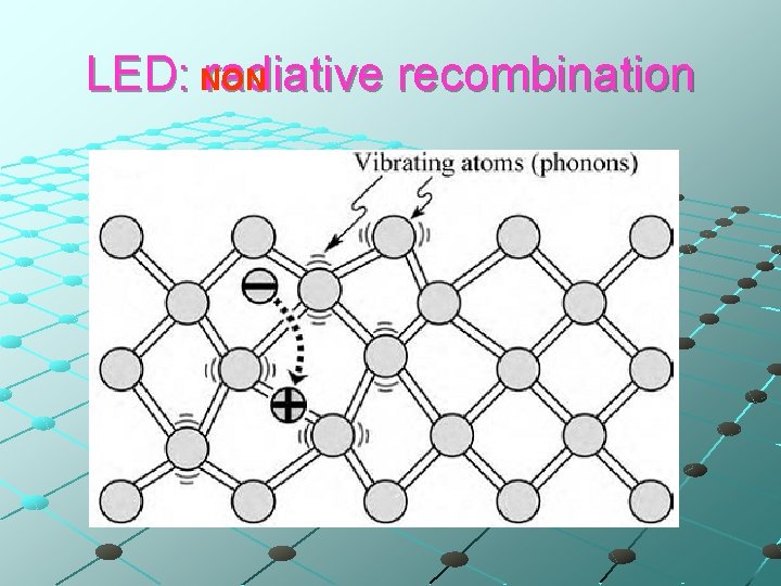
LED: NON radiative recombination

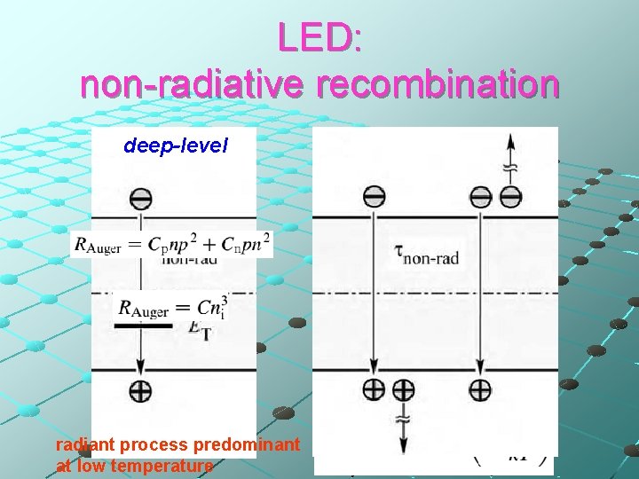
LED: non-radiative recombination deep-level radiant process predominant at low temperature Auger

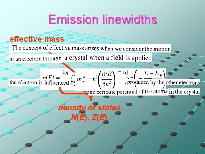
Emission linewidths effective mass density of states N(E), Z(E)

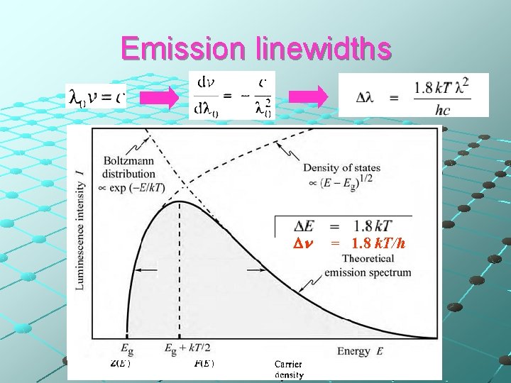
Emission linewidths Dn = 1. 8 k. T/h

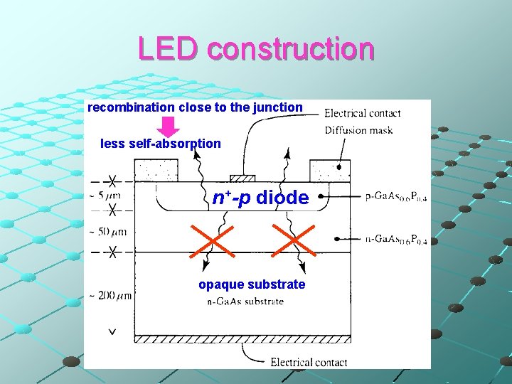
LED construction recombination close to the junction less self-absorption n+-p diode opaque substrate

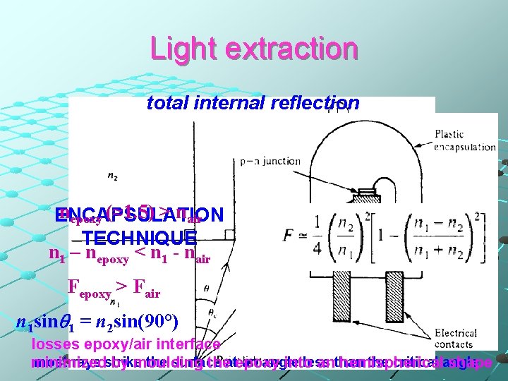
Light extraction total internal reflection nepoxy (≈1. 5) > nair ENCAPSULATION TECHNIQUE n 1 – nepoxy < n 1 - nair Fepoxy > Fair n 1 sin 1 = n 2 sin(90°) c = arcsin(n 2/n 1) losses epoxy/air interface most rays strike the surface an angle less the critical angle minimized by moulding theatepoxy into anthan hemispherical shape

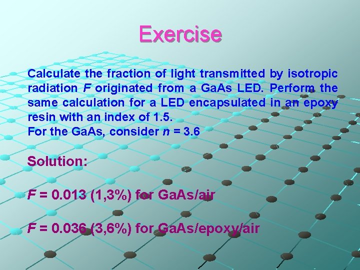
Exercise Calculate the fraction of light transmitted by isotropic radiation F originated from a Ga. As LED. Perform the same calculation for a LED encapsulated in an epoxy resin with an index of 1. 5. For the Ga. As, consider n = 3. 6 Solution: F = 0. 013 (1, 3%) for Ga. As/air F = 0. 036 (3, 6%) for Ga. As/epoxy/air

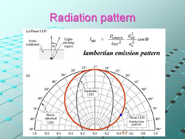
Radiation pattern 0. 5

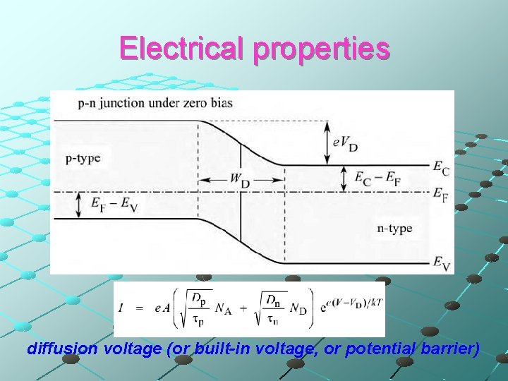
Electrical properties diffusion voltage (or built-in voltage, or potential barrier)

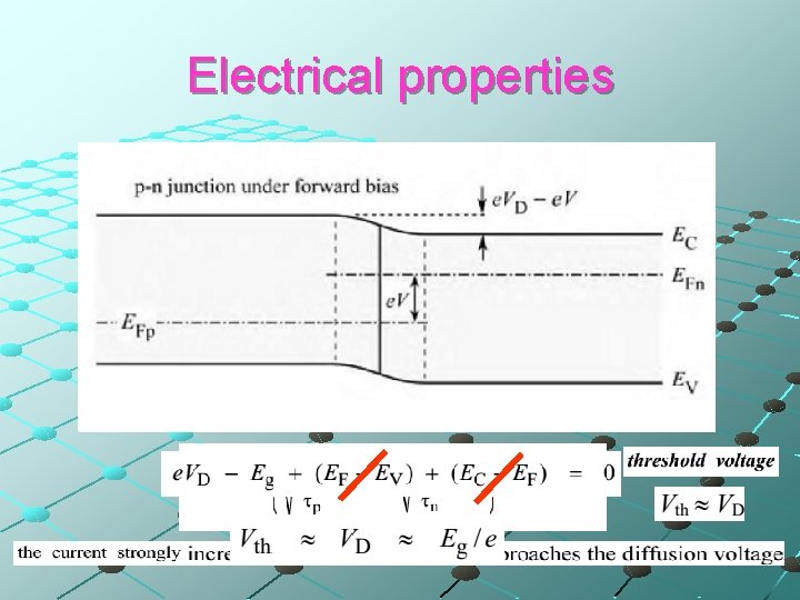
Electrical properties Eg

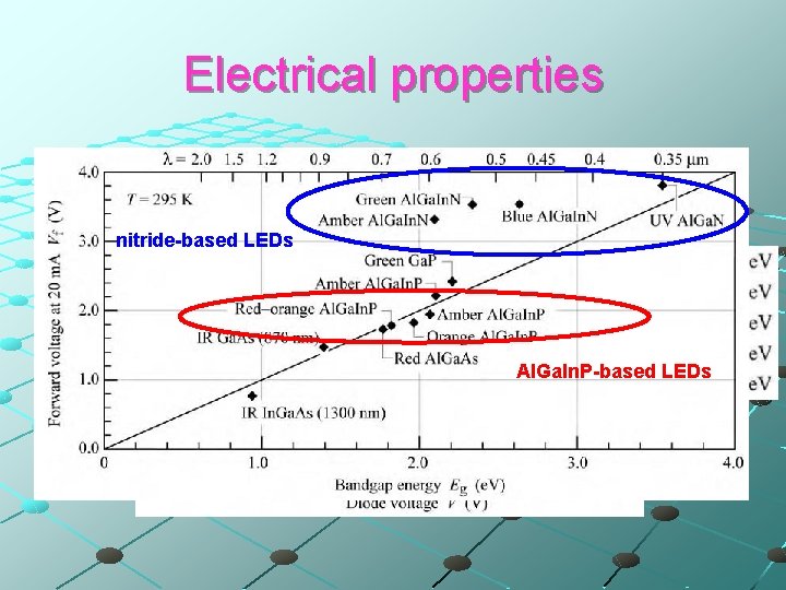
Electrical properties nitride-based LEDs Al. Ga. In. P-based LEDs

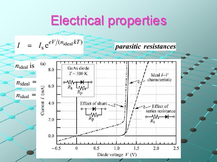
Electrical properties

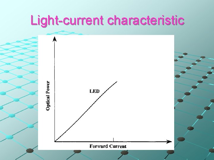
Light-current characteristic

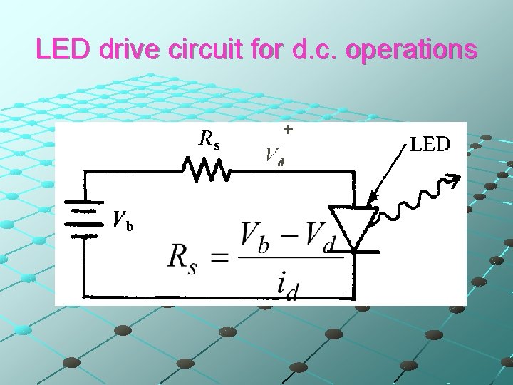
LED drive circuit for d. c. operations + Vd

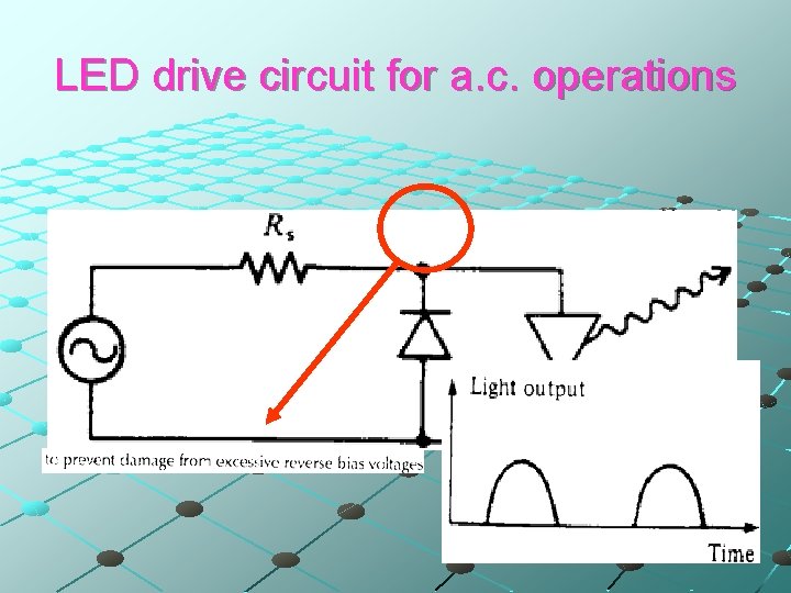
LED drive circuit for a. c. operations

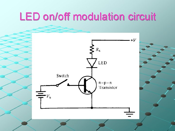
LED on/off modulation circuit

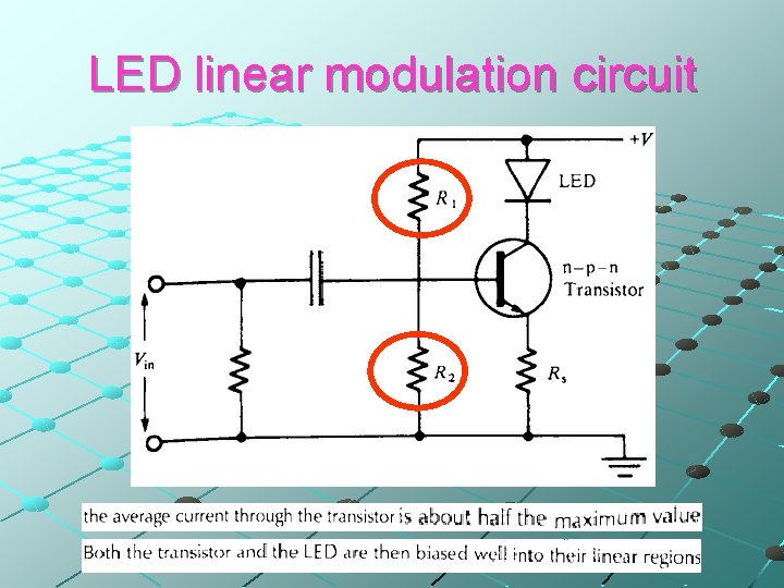
LED linear modulation circuit

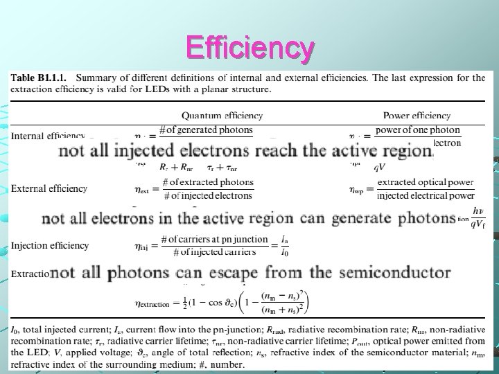
Efficiency

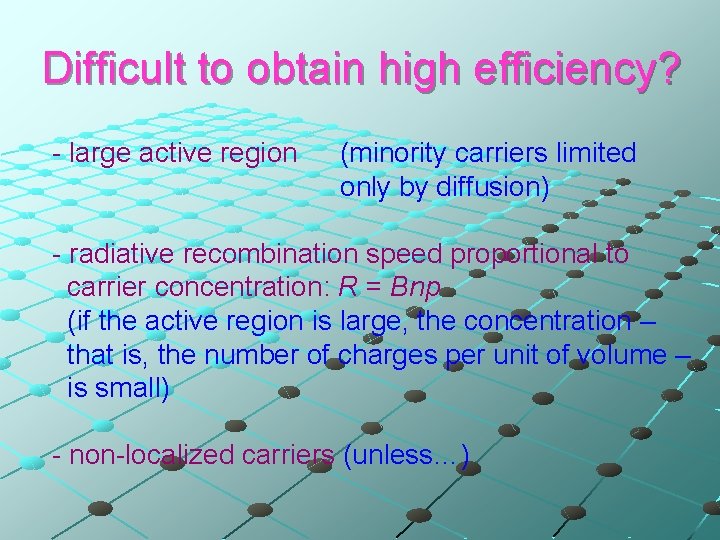
Difficult to obtain high efficiency? - large active region (minority carriers limited only by diffusion) - radiative recombination speed proportional to carrier concentration: R = Bnp (if the active region is large, the concentration – that is, the number of charges per unit of volume – is small) - non-localized carriers (unless…)

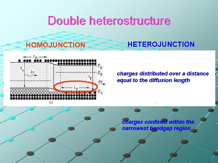
Double heterostructure HOMOJUNCTION HETEROJUNCTION charges distributed over a distance equal to the diffusion length (a) (b) charges confined within the narrowest bandgap region

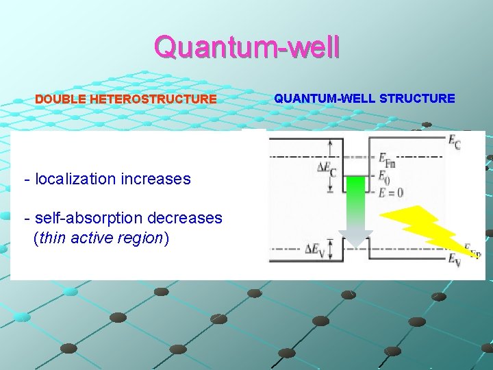
Quantum-well DOUBLE HETEROSTRUCTURE - localization increases - self-absorption decreases (thin active region) QUANTUM-WELL STRUCTURE

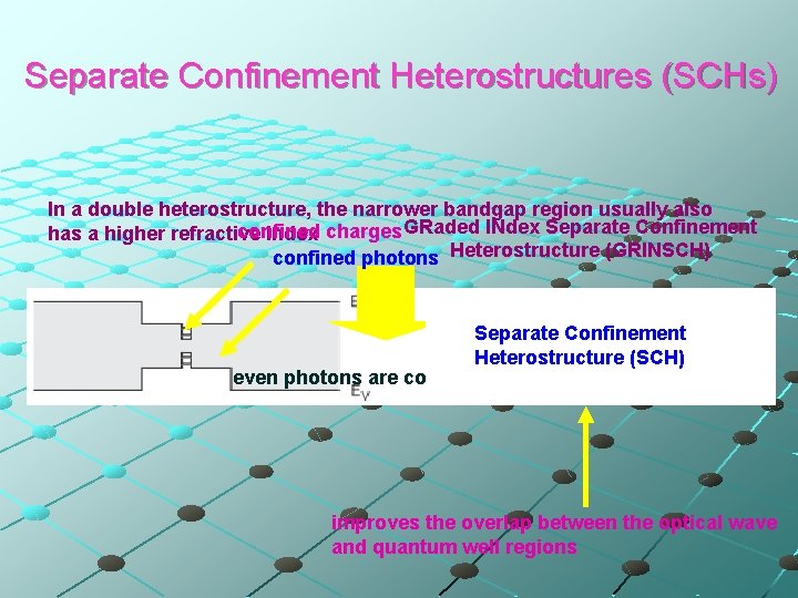
Separate Confinement Heterostructures (SCHs) In a double heterostructure, the narrower bandgap region usually also confined has a higher refractive index charges GRaded INdex Separate Confinement confined photons Heterostructure (GRINSCH) Separate Confinement Heterostructure (SCH) even photons are confined !! improves the overlap between the optical wave and quantum well regions

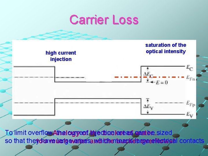
Carrier Loss high current injection saturation of the optical intensity To limit overflow, Analogy the current areas be sized of injection the bucket of can water. . . so that theytoo have largewater areas, and which large electrical contacts much themeans bucket overflows!

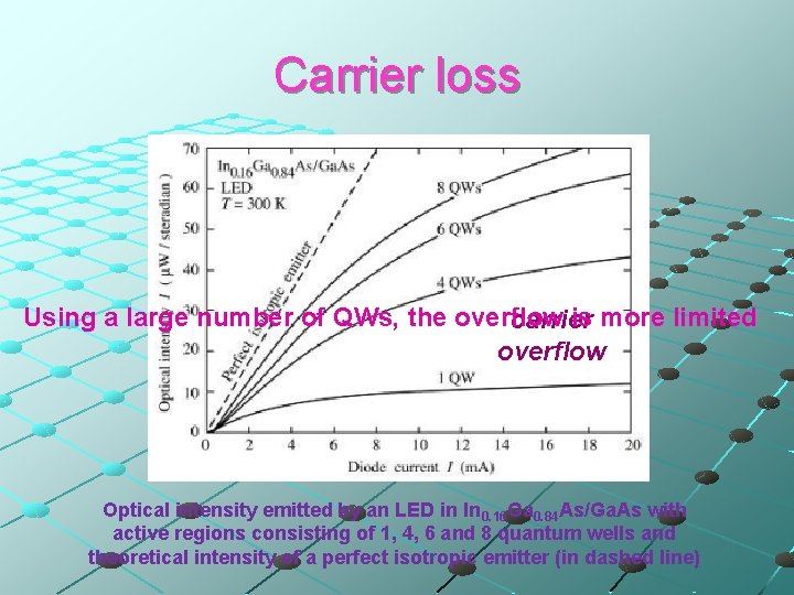
Carrier loss Using a large number of QWs, the overflow is more limited carrier overflow Optical intensity emitted by an LED in In 0. 16 Ga 0. 84 As/Ga. As with active regions consisting of 1, 4, 6 and 8 quantum wells and theoretical intensity of a perfect isotropic emitter (in dashed line)

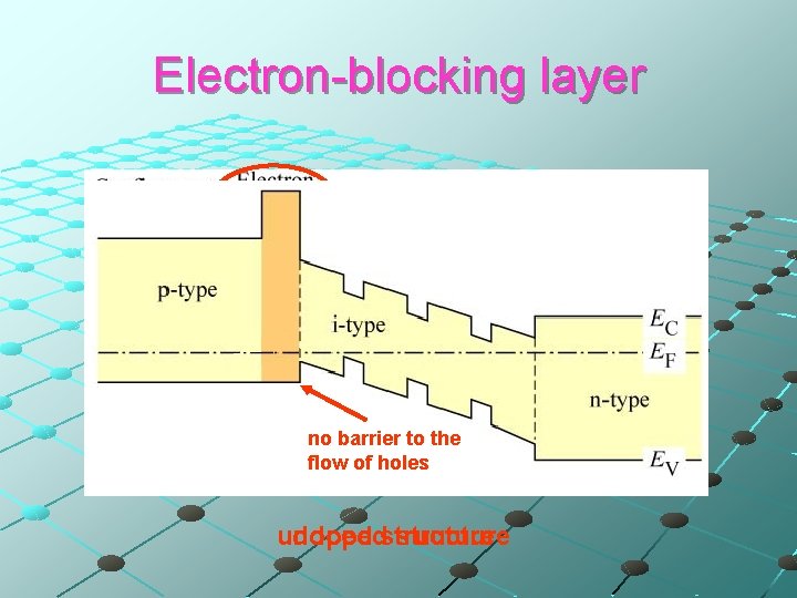
Electron-blocking layer no barrier to the flow of holes undoped structure

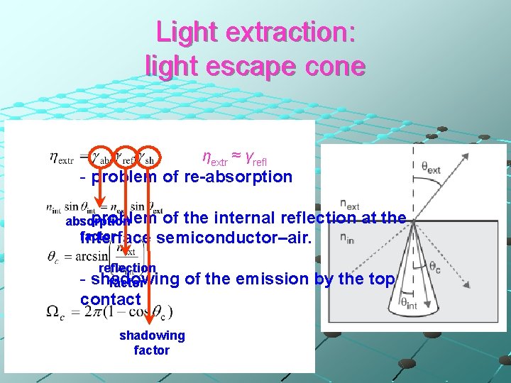
Light extraction: light escape cone ηextr ≈ γrefl - problem of re-absorption - problem of the internal reflection absorption factor interface semiconductor–air. reflection shadowing factor contact at the of the emission by the top shadowing factor

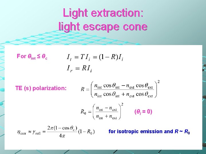
Light extraction: light escape cone For θint ≤ θc TE (s) polarization: (θi = 0) for isotropic emission and R ~ R 0

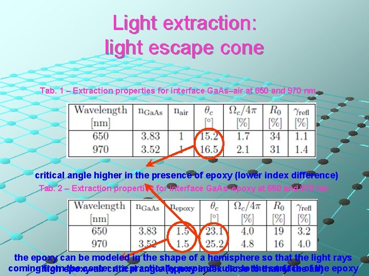
Light extraction: light escape cone Tab. 1 – Extraction properties for interface Ga. As–air at 650 and 970 nm critical angle higher in the presence of epoxy (lower index difference) Tab. 2 – Extraction properties for interface Ga. As–epoxy at 650 and 970 nm the epoxy can be modeled in the shape of a hemisphere so that the light rays coming high fromepoxy-air the centercritical are practically perpendicular to to thethat surface the epoxy angle (epoxy index close of theofair)

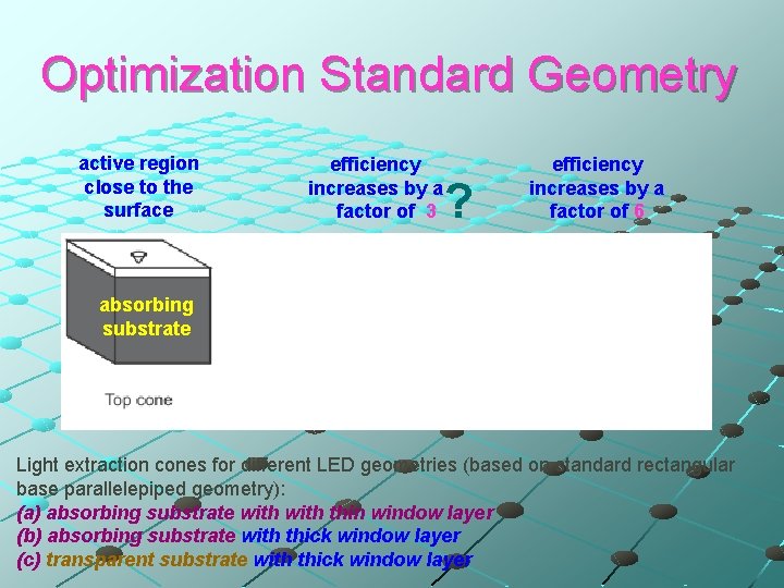
Optimization Standard Geometry active region close to the surface efficiency increases by a factor of 3 ? efficiency increases by a factor of 6 absorbing substrate Light extraction cones for different LED geometries (based on standard rectangular base parallelepiped geometry): (a) absorbing substrate with thin window layer (b) absorbing substrate with thick window layer (c) transparent substrate with thick window layer

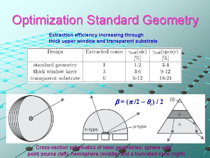
Optimization Standard Geometry Extraction efficiency increasing through thick upper window and transparent substrate = ( /2 – c) / 2 Cross-section schematics of ideal geometries; sphere with point source (left), hemisphere (middle) and a truncated cone (right)

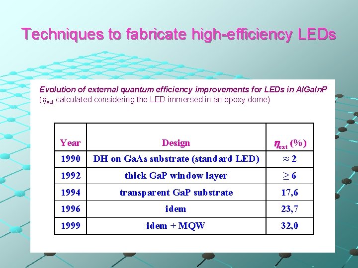
Techniques to fabricate high-efficiency LEDs Evolution of external quantum efficiency improvements for LEDs in Al. Ga. In. P (hext calculated considering the LED immersed in an epoxy dome) Year Design hext (%) 1990 DH on Ga. As substrate (standard LED) ≈2 1992 thick Ga. P window layer ≥ 6 1994 transparent Ga. P substrate 17, 6 1996 idem 23, 7 1999 idem + MQW 32, 0

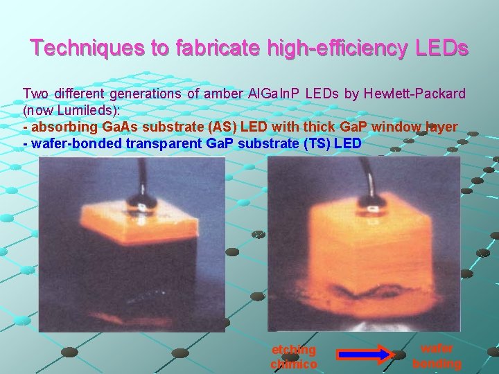
Techniques to fabricate high-efficiency LEDs Two different generations of amber Al. Ga. In. P LEDs by Hewlett-Packard (now Lumileds): - absorbing Ga. As substrate (AS) LED with thick Ga. P window layer - wafer-bonded transparent Ga. P substrate (TS) LED etching chimico wafer bonding

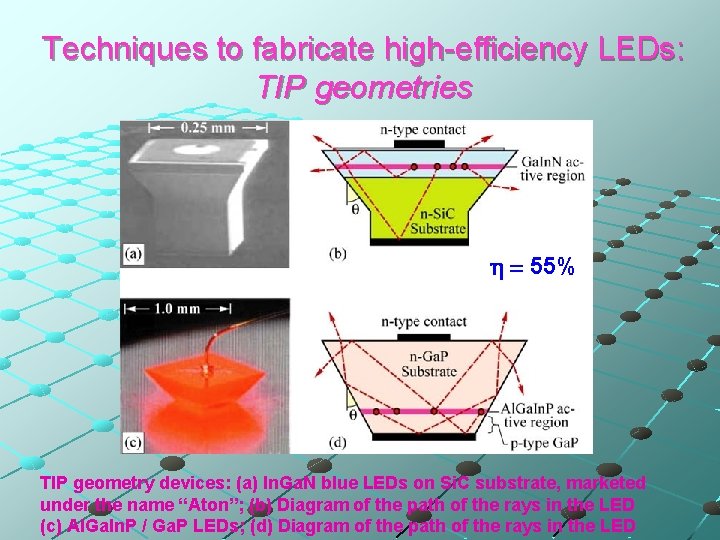
Techniques to fabricate high-efficiency LEDs: TIP geometries h = 55% TIP geometry devices: (a) In. Ga. N blue LEDs on Si. C substrate, marketed under the name “Aton”; (b) Diagram of the path of the rays in the LED (c) Al. Ga. In. P / Ga. P LEDs; (d) Diagram of the path of the rays in the LED

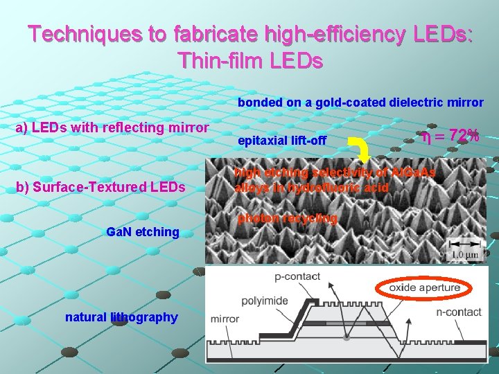
Techniques to fabricate high-efficiency LEDs: Thin-film LEDs bonded on a gold-coated dielectric mirror a) LEDs with reflecting mirror b) Surface-Textured LEDs Ga. N etching natural lithography epitaxial lift-off h = 72% high etching selectivity of Al. Ga. As alloys in hydrofluoric acid photon recycling

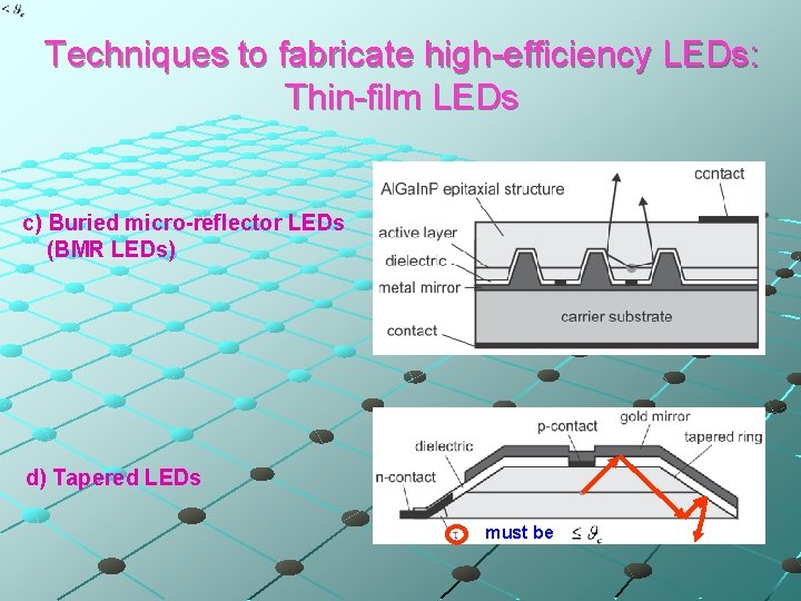
Techniques to fabricate high-efficiency LEDs: Thin-film LEDs c) Buried micro-reflector LEDs (BMR LEDs) d) Tapered LEDs must be

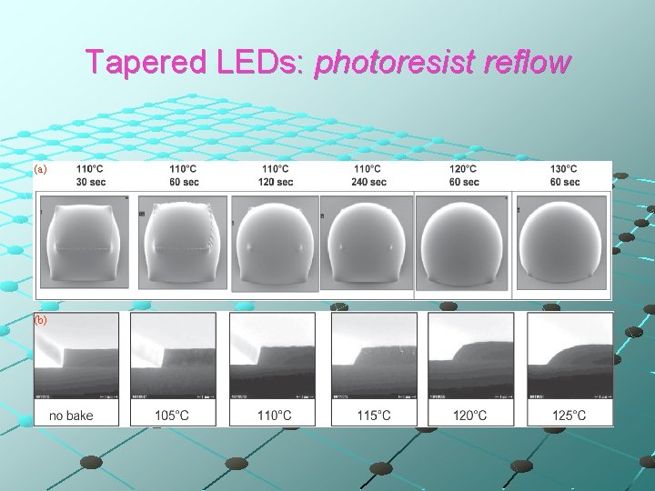
Tapered LEDs: photoresist reflow (a) (b)