Issues in Flash Memory Contents Flash Memory FTL

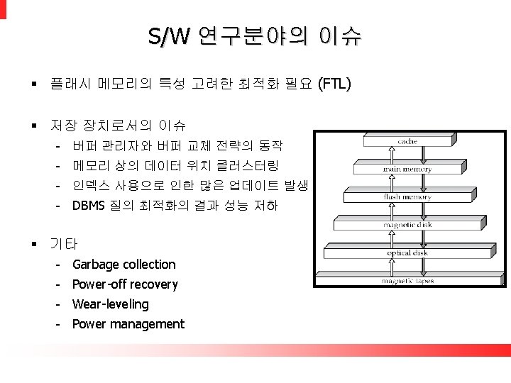
 § S/W 연구분야의 이슈")


")


 File System Read Sectors Write Sectors Mismatch! Read Write Erase")
 Memory $/Gb idle active Mobile SDRAM Low")


- Slides: 20
Issues in Flash Memory
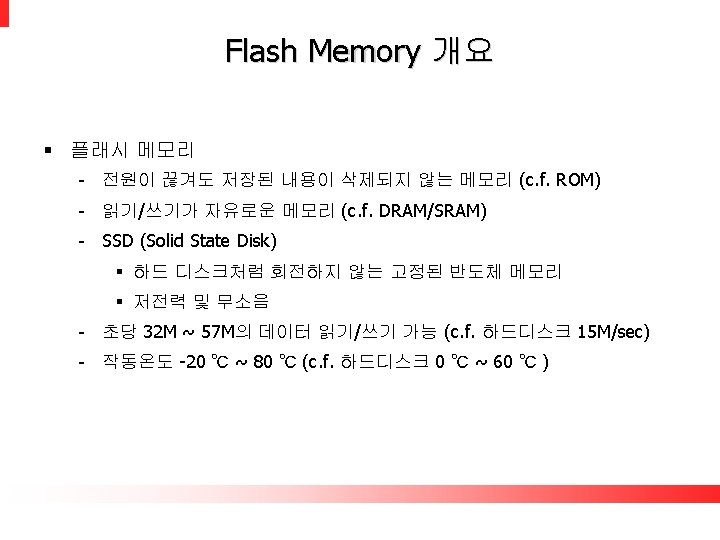
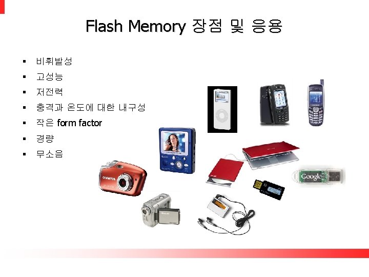
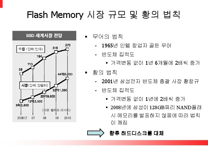
Contents § Flash Memory 개요 § FTL (Flash Translation Layer) § S/W 연구분야의 이슈
Flash Memory vs. Hard Disk Drive
NOR Flash vs. NAND Flash NOR Flash Memory 장점 NAND Flash Memory § Byte 단위 addressing § Block 단위 addressing § 빠른 read § Erase/write 성능 좋음 § 작은 cell 크기 단점 § 느린 erase/write 연산 § 느린 random access 응용 § Boot image, BIOS § Solid state disk § 대용량 저장 용도
FTL (Flash Translation Layer)
NAND Flash Memory의 구조 Page 0 Page 1 Block 0 Block 1 Block n-1 Page m-1 Device Block 0 Page 0 Block 1 Page 1 Block 2 … Block 8191 … Page 31 Page (sector) Main Array (512 B) § § § Spare Array(16 B) 1 Page = (512 + 16) Bytes 1 Block = 32 pages (sectors) 1 Device = 8192 Blocks (128 Mbytes)
Flash Memory의 특징 § Erase-before-write architecture § Erase 단위와 read/write 단위의 불일치 2 Block Page 0 Page 1 Page 2 Page 3 … Page 31 before overwrite page 1 … Page 31 Block Page 0 Page 1 Page 2 Page 3 … … Page 31 Page 1 copy & erase this block 1 Page 0 … Page 31 after overwrite page 1
FTL (Flash Translation Layer) File System Read Sectors Write Sectors Mismatch! Read Write Erase File System Read Sectors Write Sectors FTL + Device Driver + + Flash Memory HDD 출처: 지인정보기술
Memory 장치의 특성 Cost Current (m. A) Memory $/Gb idle active Mobile SDRAM Low power SRAM Fast SRAM NOR NAND 48 320 614 96 21 0. 5 0. 005 5 0. 03 0. 01 75 3 65 32 10 Random Access (16 bit) read write erase 90 ns 55 ns 10 ns 200 ns 10. 1 us 90 ns 55 ns 10 ns 210. 5 us 200. 5 us N. A 1. 2 sec 2 ms Asymmetrical operations: read/write [박찬익, 삼성전자]
Sector Mapping LSN: Logical Sector Number PSN : Physical Sector Number Sector 0 LSN PSN “Write to LSN=9” 0 12 1 11 2 10 3 9 4 8 5 7 6 6 7 5 8 4 9 3 10 2 11 1 12 0 Mapping table Sector 1 Block 0 … Block 1 Block 2 Block 3 Sector 15 Flash Memory
Block Mapping LBN: Logical Block Number PBN : Physical Block Number Sector 0 Sector 1 “Write to LSN=9” Block 0 … Block 1 LBN PBN LBN : 9/4 =2 Offset : 1 0 3 1 2 2 1 3 0 Mapping table Block 2 PBN : 1 Offset : 1 Block 3 Sector 15 Flash Memory
Hybrid Mapping LBN: Logical Block Number PBN : Physical Block Number Sector 0 Sector 1 Block 0 … “Write to LSN=9” Block 1 LBN PBN LBN : 9/4 =2 Offset : 1 0 3 1 2 2 1 3 0 Mapping table 1 Block 2 PBN : 1 Offset : 1 Block 3 Sector 15 Flash Memory
Spare Space 기법 § Mitsubishi - Data space : in-place - Spare space : out-of-place sector 0 sector 1 sector 2 sector 3 sector 4 sector 5 sector 6 1 data space sector 6 1 sector 7 1 Spare space write sector 1
Mirror Block 기법 § M-Systems data block sector 0 sector 1 sector 2 sector 3 sector 4 sector 5 sector 6 sector 7 sector 8 sector 9 sector 10 sector 11 write sector 1 mirror block sector 1 write sector 1 1 mirror block sector 1 1 write sector 1