Data Retention in MLC NAND Flash Memory Characterization




![Characterization Methodology FPGA-based flash memory testing platform [Cai+, FCCM ‘ 11] 19 Characterization Methodology FPGA-based flash memory testing platform [Cai+, FCCM ‘ 11] 19](https://slidetodoc.com/presentation_image/27e088ecad56ce3413fce0f1446ca4b0/image-19.jpg)


- Slides: 53

Data Retention in MLC NAND Flash Memory: Characterization, Optimization, and Recovery Yu Cai, Yixin Luo, Erich F. Haratsch*, Ken Mai, Onur Mutlu Carnegie Mellon University, *LSI Corporation 1

You Probably Know • Many use cases: + High performance, low energy consumption 2

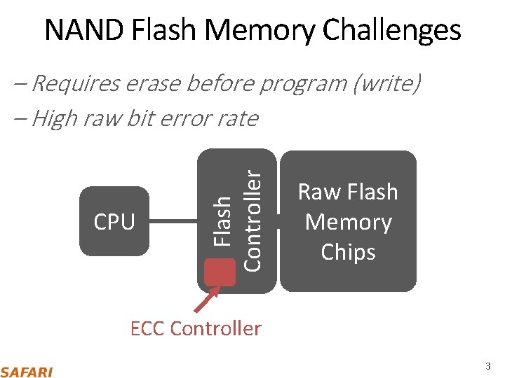
NAND Flash Memory Challenges CPU Flash Controller – Requires erase before program (write) – High raw bit error rate Raw Flash Memory Chips ECC Controller 3

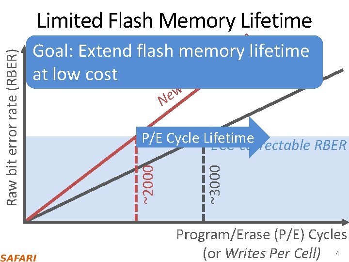
n o i t lifetime Goal: Extend flash memory a r e n e g at low cost r e w e N ~3000 P/E Cycle Lifetime ECC-correctable RBER ~2000 Raw bit error rate (RBER) Limited Flash Memory Lifetime Program/Erase (P/E) Cycles (or Writes Per Cell) 4

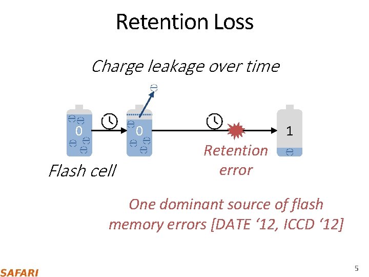
Retention Loss Charge leakage over time 0 0 Flash cell 1 Retention error One dominant source of flash memory errors [DATE ‘ 12, ICCD ‘ 12] 5

Before I show you how we extend flash lifetime … NAND Flash 101 6

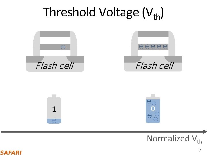
Threshold Voltage (Vth) Flash cell 1 0 Normalized Vth 7

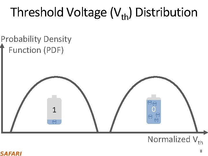
Threshold Voltage (Vth) Distribution Probability Density Function (PDF) 1 0 Normalized Vth 8

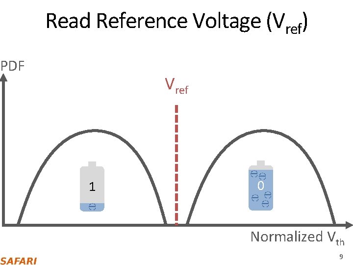
Read Reference Voltage (Vref) PDF Vref 1 0 Normalized Vth 9

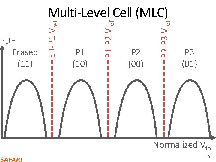
P 2 (00) P 2‐P 3 Vref P 1 (10) P 1‐P 2 Vref ER‐P 1 Vref PDF Erased (11) Multi‐Level Cell (MLC) P 3 (01) Normalized Vth 10

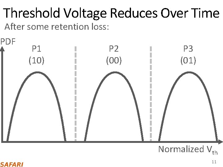
Threshold Voltage Reduces Over Time Before After some retention loss: PDF P 1 (10) P 2 (00) P 3 (01) Normalized Vth 11

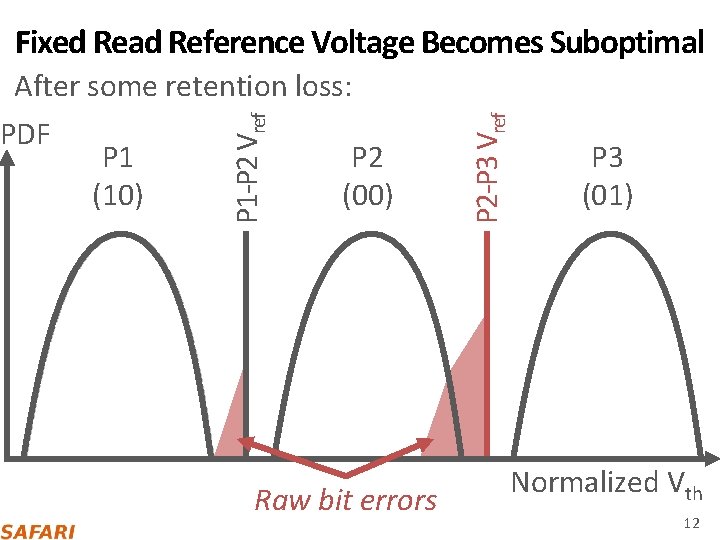
Fixed Read Reference Voltage Becomes Suboptimal P 1 (10) P 2 (00) Raw bit errors P 2‐P 3 Vref PDF P 1‐P 2 Vref Before After some retention loss: P 3 (01) Normalized Vth 12

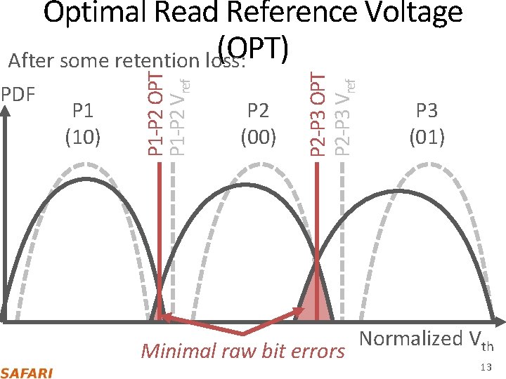
P 1 (10) P 2 (00) P 2‐P 3 OPT P 2‐P 3 Vref PDF P 1‐P 2 OPT P 1‐P 2 Vref Optimal Read Reference Voltage (OPT) After some retention loss: Minimal raw bit errors P 3 (01) Normalized Vth 13

Goal 1: Design a low‐cost mechanism that dynamically finds the optimal read reference voltage 14

Retention Failure P 1 (10) P 2 (00) P 2‐P 3 Vref PDF P 1‐P 2 Vref some retention loss: After significant retention Uncorrectable errors Correctable errors P 3 (01) Normalized Vth 15

Goal 1: Design a low‐cost mechanism that dynamically finds the optimal read reference voltage Goal 2: Design an offline mechanism to recover data after detecting uncorrectable errors 16

To understand the effects of retention loss: ‐ Characterize retention loss using real chips 17

To understand the effects of retention loss: ‐ Characterize retention loss using real chips Goal 1: Design a low‐cost mechanism that dynamically finds the optimal read reference voltage Goal 2: Design an offline mechanism to recover data after detecting uncorrectable errors 18
![Characterization Methodology FPGAbased flash memory testing platform Cai FCCM 11 19 Characterization Methodology FPGA-based flash memory testing platform [Cai+, FCCM ‘ 11] 19](https://slidetodoc.com/presentation_image/27e088ecad56ce3413fce0f1446ca4b0/image-19.jpg)
Characterization Methodology FPGA-based flash memory testing platform [Cai+, FCCM ‘ 11] 19

Characterization Methodology • FPGA-based flash memory testing platform • Real 20 - to 24 -nm MLC NAND flash chips • 0 - to 40 -day worth of retention loss • Room temperature (20⁰C) • 0 to 50 k P/E Cycles 20

Characterize the effects of retention loss 1. Threshold Voltage Distribution 2. Optimal Read Reference Voltage 3. RBER and P/E Cycle Lifetime 21

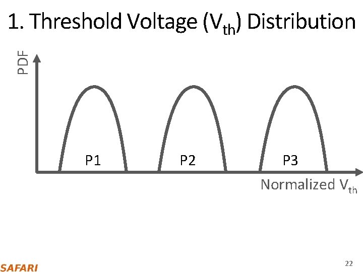
PDF 1. Threshold Voltage (Vth) Distribution P 1 P 2 P 3 Normalized Vth 22

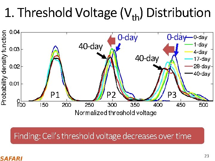
1. Threshold Voltage (Vth) Distribution 0‐day 40‐day P 1 P 2 P 3 Finding: Cell’s threshold voltage decreases over time 23

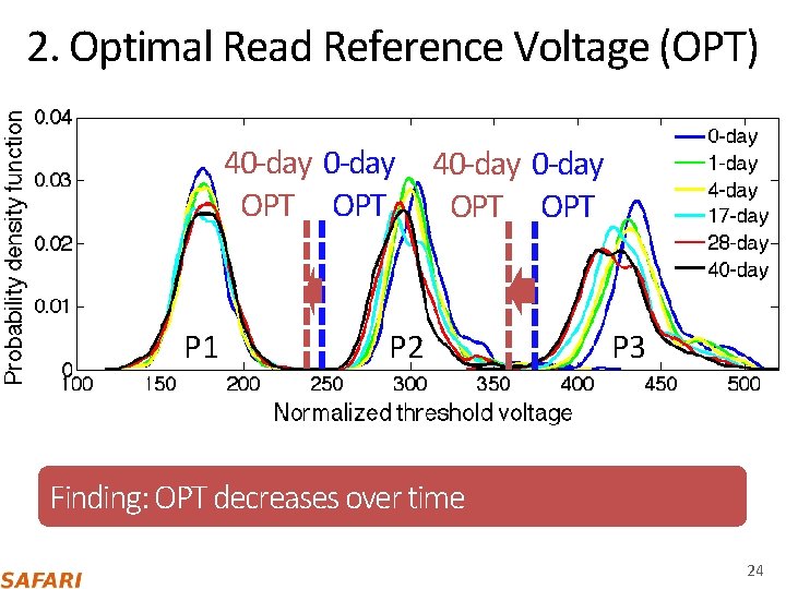
2. Optimal Read Reference Voltage (OPT) 40‐day OPT P 1 40‐day OPT P 2 P 3 Finding: OPT decreases over time 24

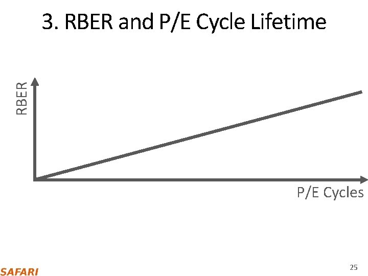
RBER 3. RBER and P/E Cycle Lifetime P/E Cycles 25

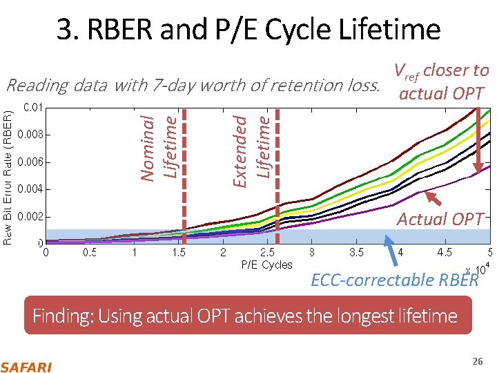
3. RBER and P/E Cycle Lifetime Extended Lifetime Nominal Lifetime Vref closer to Reading data with 7 -day worth of retention loss. actual OPT Actual OPT ECC-correctable RBER Finding: Using actual OPT achieves the longest lifetime 26

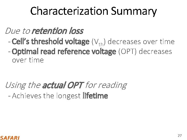
Characterization Summary Due to retention loss ‐ Cell’s threshold voltage (Vth) decreases over time ‐ Optimal read reference voltage (OPT) decreases over time Using the actual OPT for reading ‐ Achieves the longest lifetime 27

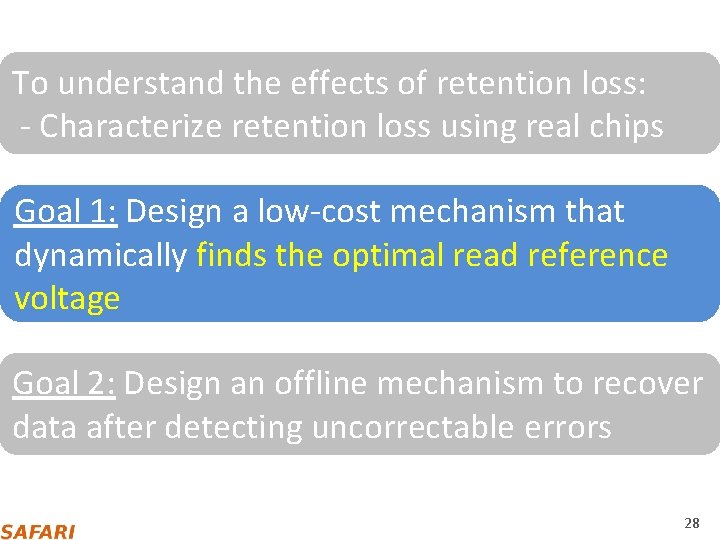
To understand the effects of retention loss: ‐ Characterize retention loss using real chips Goal 1: Design a low‐cost mechanism that dynamically finds the optimal read reference voltage Goal 2: Design an offline mechanism to recover data after detecting uncorrectable errors 28

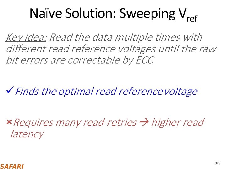
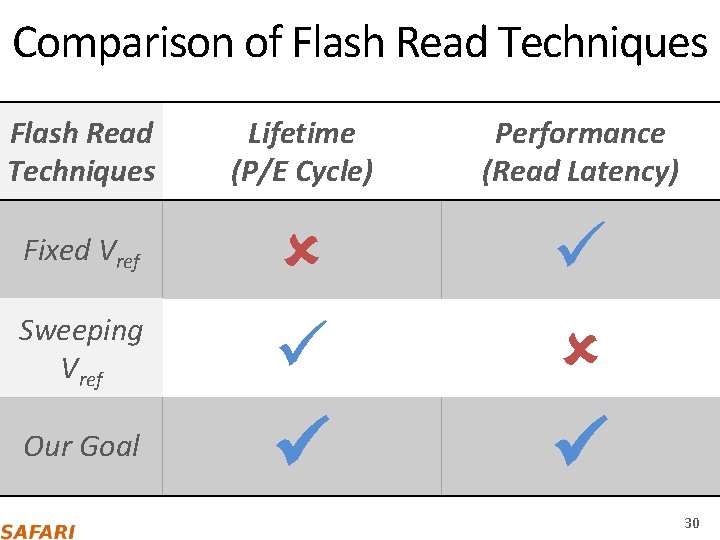
Naïve Solution: Sweeping Vref Key idea: Read the data multiple times with different read reference voltages until the raw bit errors are correctable by ECC Finds the optimal read reference voltage Requires many read-retries higher read latency 29

Comparison of Flash Read Techniques Fixed Vref Sweeping Vref Our Goal Lifetime (P/E Cycle) Performance (Read Latency) 30

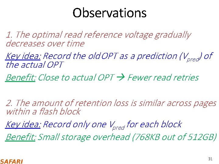
Observations 1. The optimal read reference voltage gradually decreases over time Key idea: Record the old OPT as a prediction (Vpred) of the actual OPT Benefit: Close to actual OPT Fewer read retries 2. The amount of retention loss is similar across pages within a flash block Key idea: Record only one Vpred for each block Benefit: Small storage overhead (768 KB out of 512 GB) 31

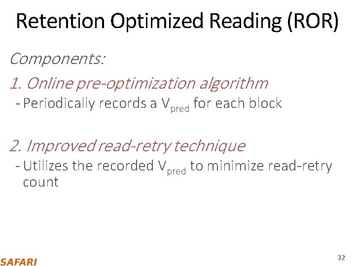
Retention Optimized Reading (ROR) Components: 1. Online pre-optimization algorithm ‐ Periodically records a Vpred for each block 2. Improved read-retry technique ‐ Utilizes the recorded Vpred to minimize read-retry count 32

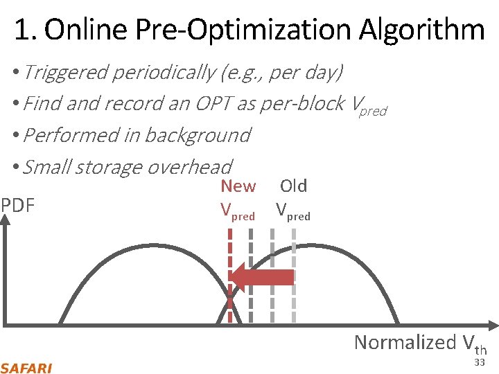
1. Online Pre‐Optimization Algorithm • Triggered periodically (e. g. , per day) • Find and record an OPT as per-block Vpred • Performed in background • Small storage overhead PDF New Vpred Old Vpred Normalized Vth 33

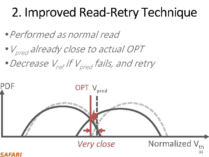
2. Improved Read‐Retry Technique • Performed as normal read • Vpred already close to actual OPT • Decrease Vref if Vpred fails, and retry PDF OPT Vpred Very close Normalized Vth 34

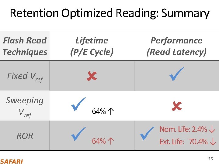
Retention Optimized Reading: Summary Flash Read Techniques Fixed Vref Sweeping Vref ROR Lifetime (P/E Cycle) 64% ↑ Performance (Read Latency) _____ Nom. Life: 2. 4% ↓ Ext. Life: 70. 4% ↓ 35

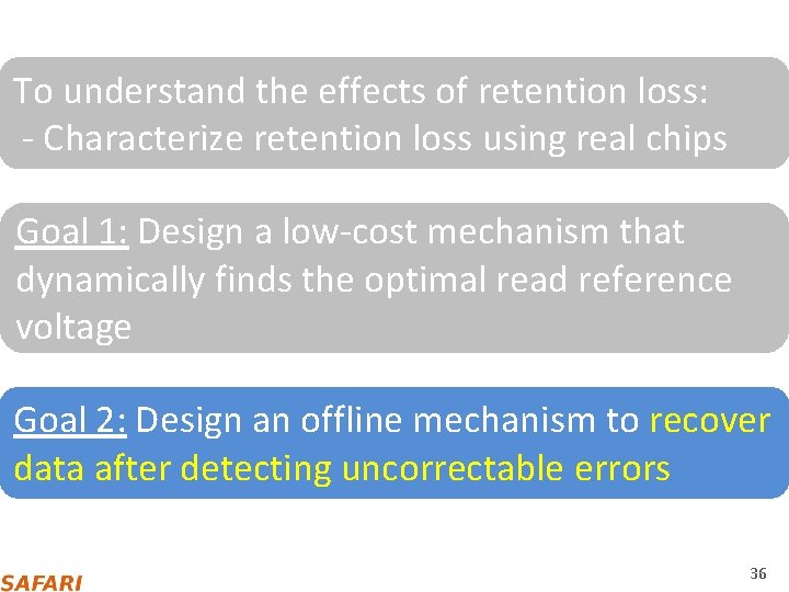
To understand the effects of retention loss: ‐ Characterize retention loss using real chips Goal 1: Design a low‐cost mechanism that dynamically finds the optimal read reference voltage Goal 2: Design an offline mechanism to recover data after detecting uncorrectable errors 36

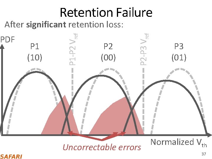
Retention Failure P 1 (10) P 2 (00) P 2‐P 3 Vref PDF P 1‐P 2 Vref After some significant retention After retention loss: Uncorrectable errors Correctable errors P 3 (01) Normalized Vth 37

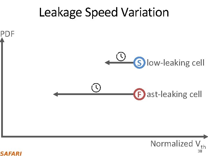
Leakage Speed Variation PDF S low‐leaking cell F ast‐leaking cell Normalized Vth 38

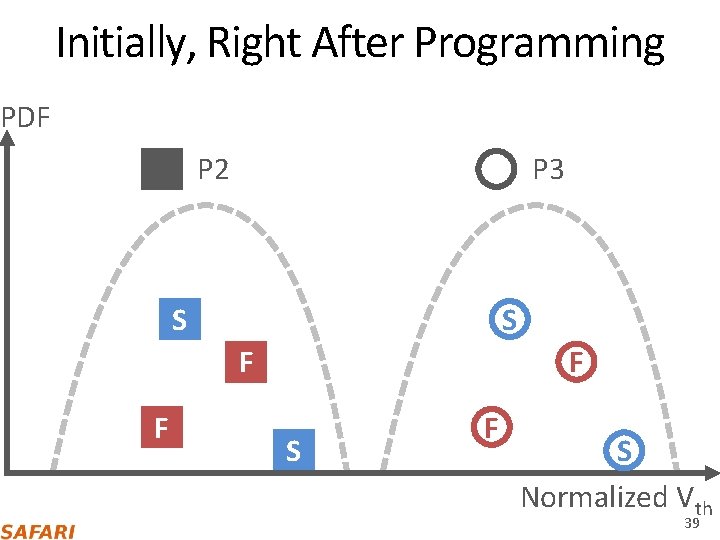
Initially, Right After Programming PDF P 2 P 3 S S F F F S Normalized Vth 39

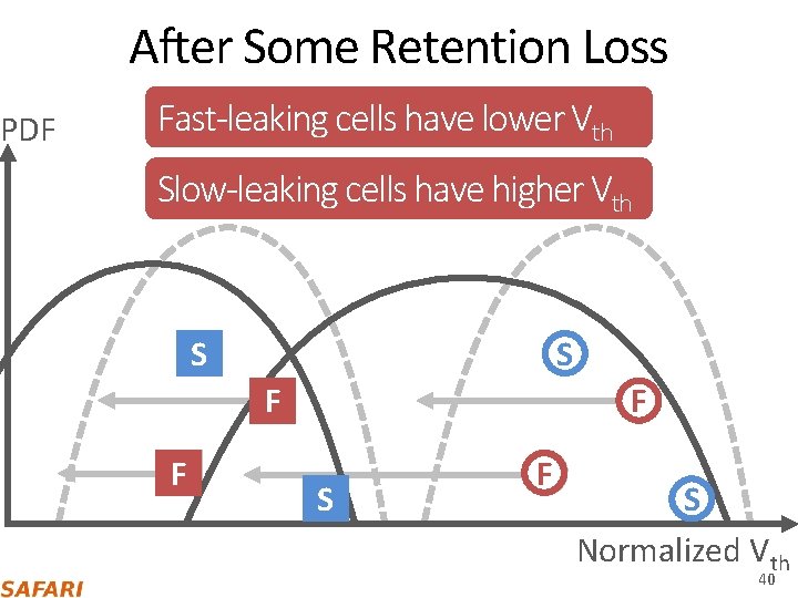
PDF After Some Retention Loss Fast-leaking cells have lower Vth P 2 Slow-leaking cells have higher P 3 Vth S S F F F S Normalized Vth 40

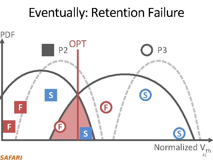
Eventually: Retention Failure PDF P 2 OPT P 3 S S F F S S Normalized Vth 41

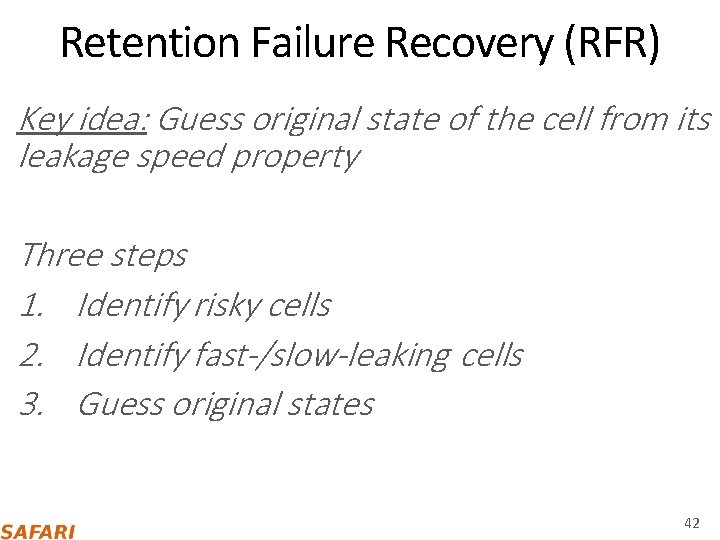
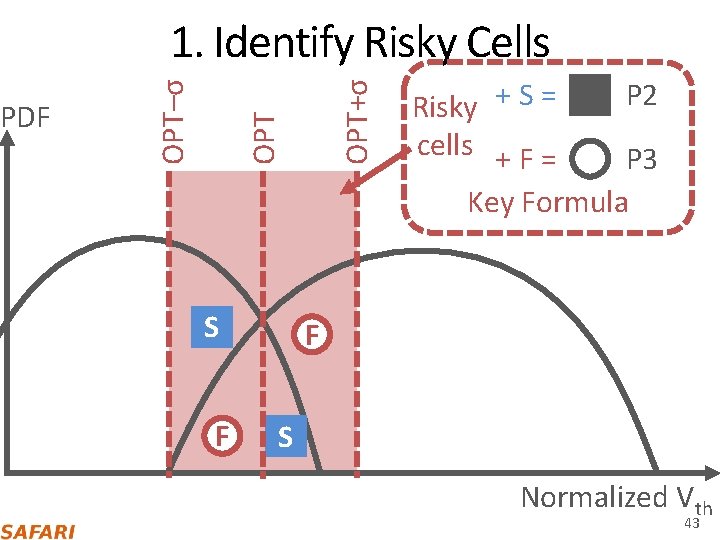
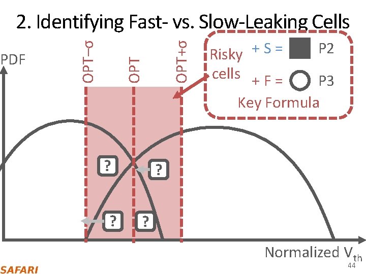
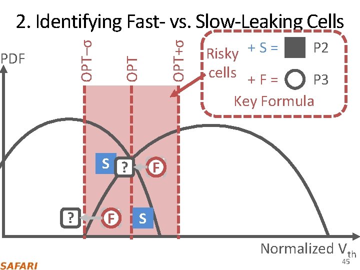
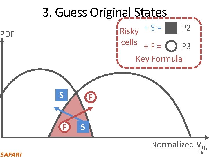
Retention Failure Recovery (RFR) Key idea: Guess original state of the cell from its leakage speed property Three steps 1. Identify risky cells 2. Identify fast-/slow-leaking cells 3. Guess original states 42

OPT+σ OPT–σ PDF 1. Identify Risky Cells S F P 2 Risky + S = cells + F = P 3 Key Formula F S Normalized Vth 43

OPT+σ OPT PDF OPT–σ 2. Identifying Fast‐ vs. Slow‐Leaking Cells ? ? P 2 Risky + S = cells + F = P 3 Key Formula ? ? Normalized Vth 44

S? ? ? OPT+σ PDF OPT–σ 2. Identifying Fast‐ vs. Slow‐Leaking Cells ? F P 2 Risky + S = cells + F = P 3 Key Formula ? F S? Normalized Vth 45

3. Guess Original States P 2 Risky + S = cells + F = P 3 Key Formula PDF S F F S Normalized Vth 46

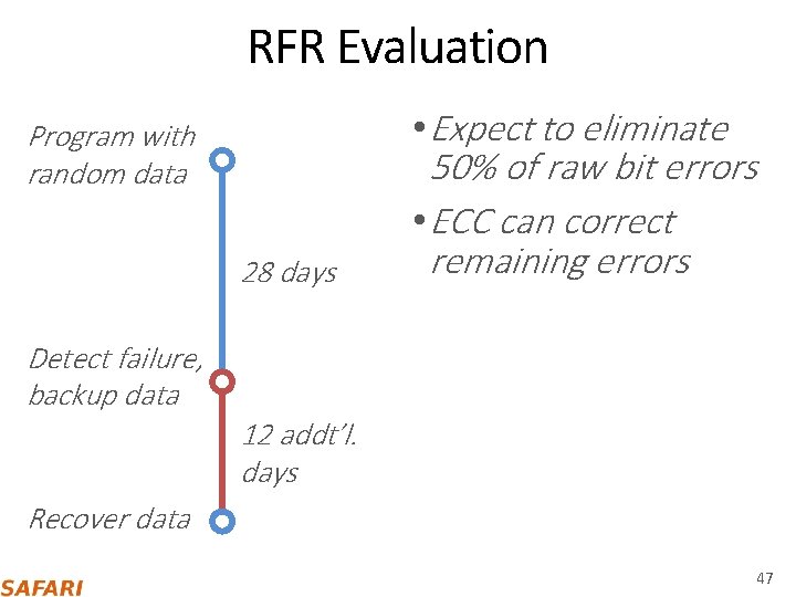
RFR Evaluation Program with random data 28 days Detect failure, backup data • Expect to eliminate 50% of raw bit errors • ECC can correct remaining errors 12 addt’l. days Recover data 47

To understand the effects of retention loss: ‐ Characterize retention loss using real chips Goal 1: Design a low‐cost mechanism that dynamically finds the optimal read reference voltage Goal 2: Design an offline mechanism to recover data after detecting uncorrectable errors 48

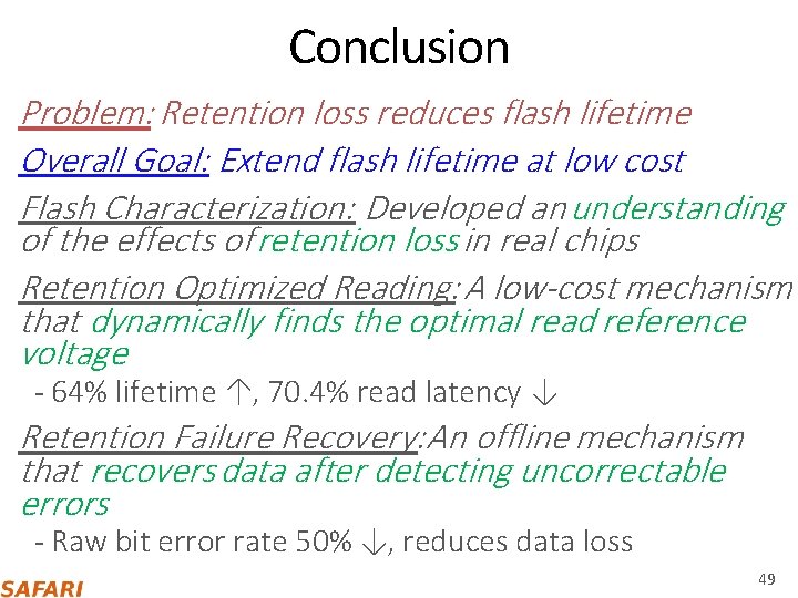
Conclusion Problem: Retention loss reduces flash lifetime Overall Goal: Extend flash lifetime at low cost Flash Characterization: Developed an understanding of the effects of retention loss in real chips Retention Optimized Reading: A low-cost mechanism that dynamically finds the optimal read reference voltage ‐ 64% lifetime ↑, 70. 4% read latency ↓ Retention Failure Recovery: An offline mechanism that recovers data after detecting uncorrectable errors ‐ Raw bit error rate 50% ↓, reduces data loss 49

Data Retention in MLC NAND Flash Memory: Characterization, Optimization, and Recovery Yu Cai, Yixin Luo, Erich F. Haratsch*, Ken Mai, Onur Mutlu Carnegie Mellon University, *LSI Corporation 50

Backup Slides 51

RFR Motivation Data loss can happen in many ways 1. High P/E cycle 2. High temperature accelerates retention loss 3. High retention age (lost power for a long time) 52

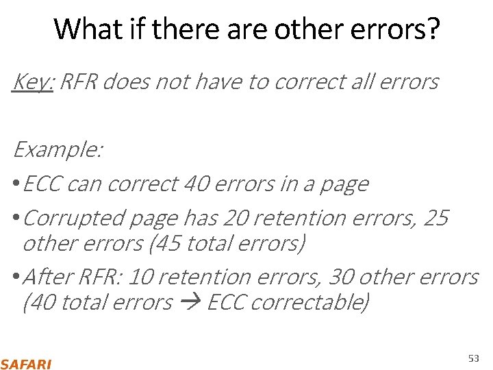
What if there are other errors? Key: RFR does not have to correct all errors Example: • ECC can correct 40 errors in a page • Corrupted page has 20 retention errors, 25 other errors (45 total errors) • After RFR: 10 retention errors, 30 other errors (40 total errors ECC correctable) 53