INTRODUCTION TO THE ARM PROCESSOR 353156 Microprocessor Asst
![What is “Instruction Set Architecture (ISA)” The attributes of [computing] system as seen by What is “Instruction Set Architecture (ISA)” The attributes of [computing] system as seen by](https://slidetodoc.com/presentation_image/35df1d0fe44c3641eafb7e1256daa7c7/image-4.jpg)
- Slides: 22

INTRODUCTION TO THE ARM PROCESSOR 353156 – Microprocessor Asst. Prof. Dr. Choopan Rattanapoka and Asst. Prof. Dr. Suphot Chunwiphat

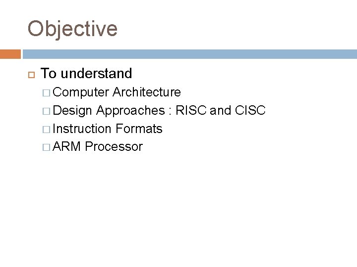
Objective To understand � Computer Architecture � Design Approaches : RISC and CISC � Instruction Formats � ARM Processor

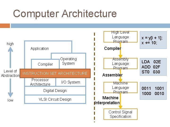
Computer Architecture High Level Language Program high Compiler Application Compiler Operating System Level of INSTRUCTION SET ARCHITECTURE Abstraction Processor I/O System Architecture Digital Design low x = y[i + 1]; x += 10; VLSI Circuit Design Assembly Language Program Assembler Machine Language Program Machine Interpretation Control Signal Specification LDA 02 E ADD 02 F ST 0 030 0011 1000 0010
![What is Instruction Set Architecture ISA The attributes of computing system as seen by What is “Instruction Set Architecture (ISA)” The attributes of [computing] system as seen by](https://slidetodoc.com/presentation_image/35df1d0fe44c3641eafb7e1256daa7c7/image-4.jpg)
What is “Instruction Set Architecture (ISA)” The attributes of [computing] system as seen by the programmer. i. e. the conceptual structure and functional behavior, as distinct from the organization of the data flows and controls the logic design, and the physical implementation. ISA includes : Organization of Programmable Storage � Data Types and Data Structures: Encoding & Representation � Instruction Formats � Instruction (or Operation Code) Set � Modes of Addressing and Accessing Data Items and Instructions � Exceptional Conditions �

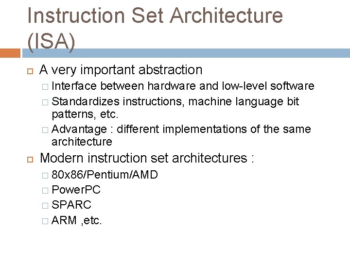
Instruction Set Architecture (ISA) A very important abstraction � Interface between hardware and low-level software � Standardizes instructions, machine language bit patterns, etc. � Advantage : different implementations of the same architecture Modern instruction set architectures : � 80 x 86/Pentium/AMD � Power. PC � SPARC � ARM , etc.

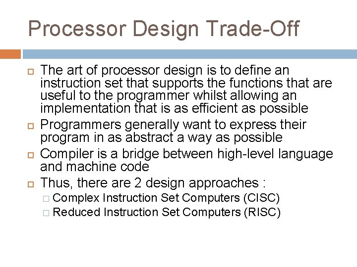
Processor Design Trade-Off The art of processor design is to define an instruction set that supports the functions that are useful to the programmer whilst allowing an implementation that is as efficient as possible Programmers generally want to express their program in as abstract a way as possible Compiler is a bridge between high-level language and machine code Thus, there are 2 design approaches : � Complex Instruction Set Computers (CISC) � Reduced Instruction Set Computers (RISC)

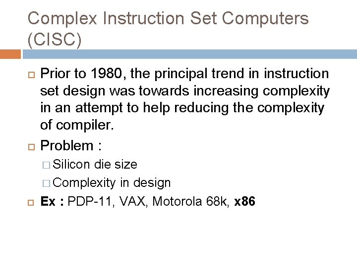
Complex Instruction Set Computers (CISC) Prior to 1980, the principal trend in instruction set design was towards increasing complexity in an attempt to help reducing the complexity of compiler. Problem : � Silicon die size � Complexity in design Ex : PDP-11, VAX, Motorola 68 k, x 86

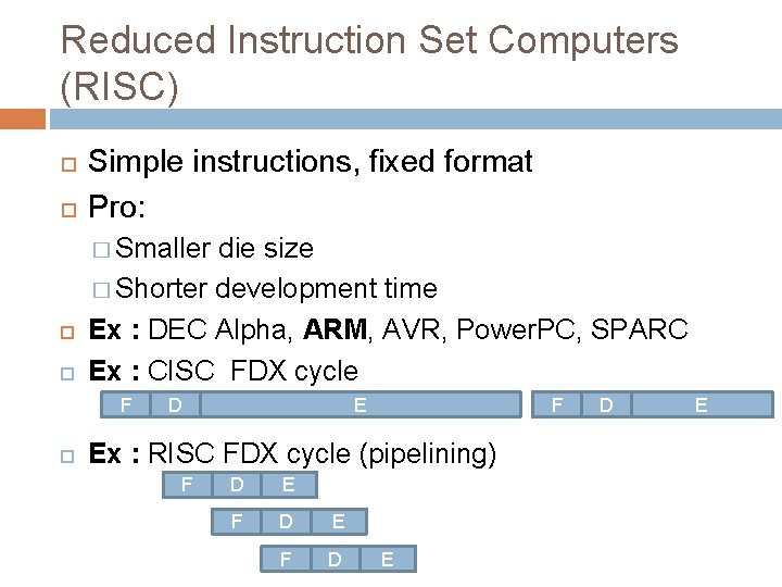
Reduced Instruction Set Computers (RISC) Simple instructions, fixed format Pro: � Smaller die size � Shorter development time Ex : DEC Alpha, ARM, AVR, Power. PC, SPARC Ex : CISC FDX cycle F D E F Ex : RISC FDX cycle (pipelining) F D E

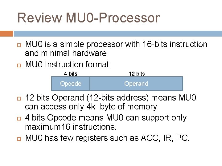
Review MU 0 -Processor MU 0 is a simple processor with 16 -bits instruction and minimal hardware MU 0 Instruction format 4 bits 12 bits Opcode Operand 12 bits Operand (12 -bits address) means MU 0 can access only 4 k byte of memory 4 bits Opcode means MU 0 can support only maximum 16 instructions. MU 0 has few registers such as ACC, IR, PC.

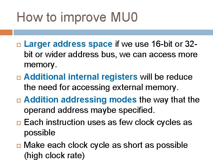
How to improve MU 0 Larger address space if we use 16 -bit or 32 bit or wider address bus, we can access more memory. Additional internal registers will be reduce the need for accessing external memory. Addition addressing modes the way that the operand address maybe specified. Each instruction uses as few clock cycles as possible Make each clock cycle as short as possible (high clock rate)

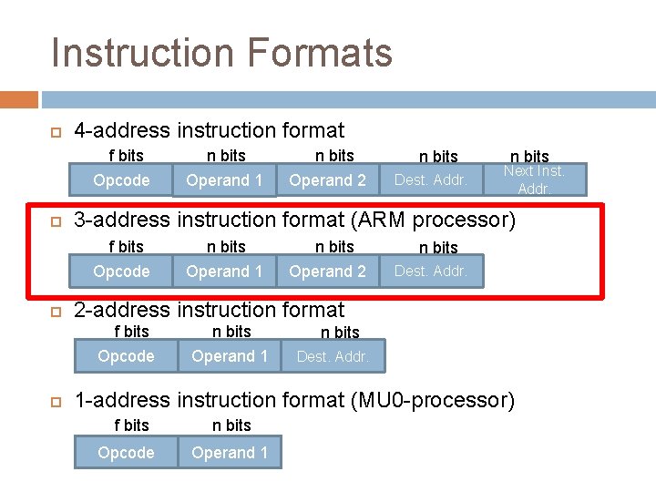
Instruction Formats 4 -address instruction format f bits Opcode n bits Dest. Addr. n bits Next Inst. Addr. n bits Operand 1 n bits Operand 2 n bits Dest. Addr. 2 -address instruction format f bits Opcode n bits Operand 2 3 -address instruction format (ARM processor) f bits Opcode n bits Operand 1 n bits Dest. Addr. 1 -address instruction format (MU 0 -processor) f bits Opcode n bits Operand 1

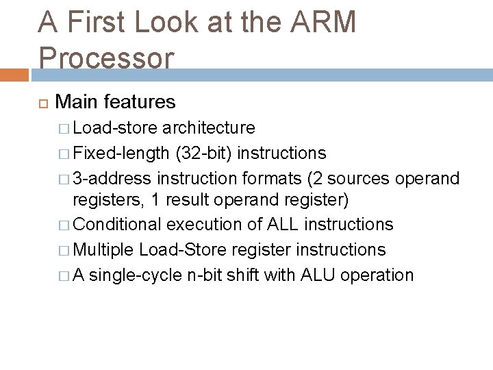
A First Look at the ARM Processor Main features � Load-store architecture � Fixed-length (32 -bit) instructions � 3 -address instruction formats (2 sources operand registers, 1 result operand register) � Conditional execution of ALL instructions � Multiple Load-Store register instructions � A single-cycle n-bit shift with ALU operation

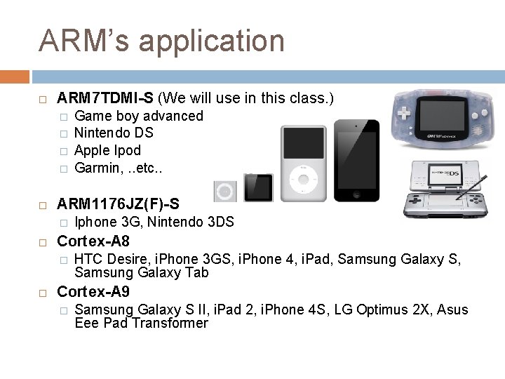
ARM’s application ARM 7 TDMI-S (We will use in this class. ) � � ARM 1176 JZ(F)-S � Iphone 3 G, Nintendo 3 DS Cortex-A 8 � Game boy advanced Nintendo DS Apple Ipod Garmin, . . etc. . HTC Desire, i. Phone 3 GS, i. Phone 4, i. Pad, Samsung Galaxy S, Samsung Galaxy Tab Cortex-A 9 � Samsung Galaxy S II, i. Pad 2, i. Phone 4 S, LG Optimus 2 X, Asus Eee Pad Transformer

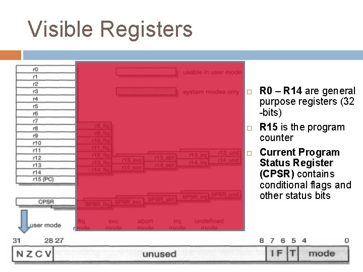
Visible Registers R 0 – R 14 are general purpose registers (32 -bits) R 15 is the program counter Current Program Status Register (CPSR) contains conditional flags and other status bits

ASSEMBLY LANGUAGE PROGRAMMING 353156 – Microprocessor Asst. Prof. Dr. Choopan Rattanapoka

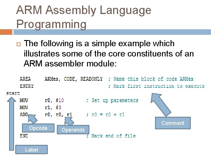
ARM Assembly Language Programming The following is a simple example which illustrates some of the core constituents of an ARM assembler module: Opcode Label Comment Operands

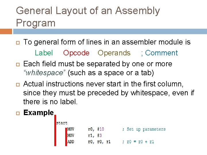
General Layout of an Assembly Program To general form of lines in an assembler module is Label Opcode Operands ; Comment Each field must be separated by one or more “whitespace” (such as a space or a tab) Actual instructions never start in the first column, since they must be preceded by whitespace, even if there is no label. Example

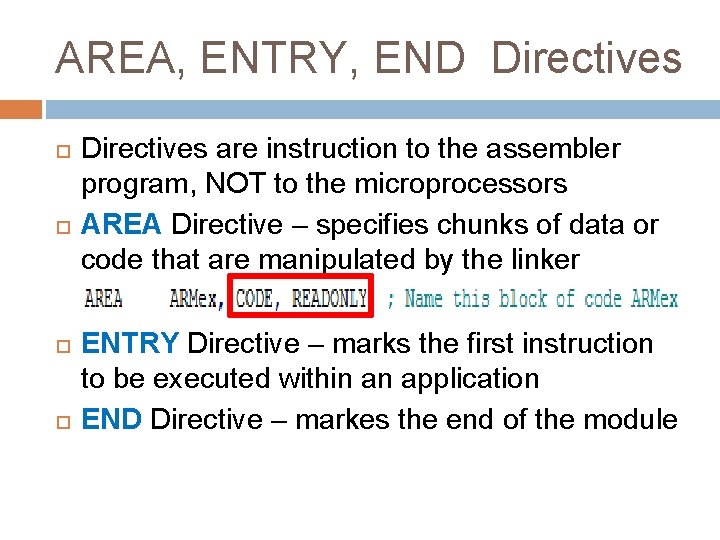
AREA, ENTRY, END Directives are instruction to the assembler program, NOT to the microprocessors AREA Directive – specifies chunks of data or code that are manipulated by the linker ENTRY Directive – marks the first instruction to be executed within an application END Directive – markes the end of the module

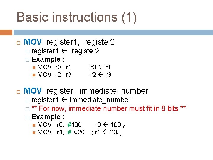
Basic instructions (1) MOV register 1, register 2 � register 1 register 2 � Example : MOV r 0, r 1 MOV r 2, r 3 ; r 0 r 1 ; r 2 r 3 MOV register, immediate_number � register 1 immediate_number � ** For now, immediate number must fit in 8 bits ** � Example : MOV r 0, #100 MOV r 1, #0 x 20 ; r 0 10010 ; r 1 2016

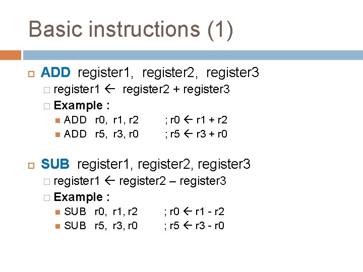
Basic instructions (1) ADD register 1, register 2, register 3 � register 1 register 2 + register 3 � Example : ADD r 0, r 1, r 2 ADD r 5, r 3, r 0 ; r 0 r 1 + r 2 ; r 5 r 3 + r 0 SUB register 1, register 2, register 3 � register 1 register 2 – register 3 � Example : SUB r 0, r 1, r 2 SUB r 5, r 3, r 0 ; r 0 r 1 - r 2 ; r 5 r 3 - r 0

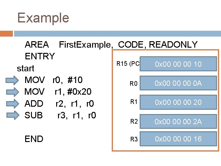
Example AREA First. Example, CODE, READONLY ENTRY R 15 (PC) 0 x 00 00 00 0 C 00 04 08 10 start MOV r 0, #10 R 0 0 x 00 00 00 0 A 00 MOV r 1, #0 x 20 R 1 0 x 00 00 00 20 00 ADD r 2, r 1, r 0 SUB r 3, r 1, r 0 END R 2 0 x 00 00 00 2 A 00 R 3 0 x 00 00 00 16 00

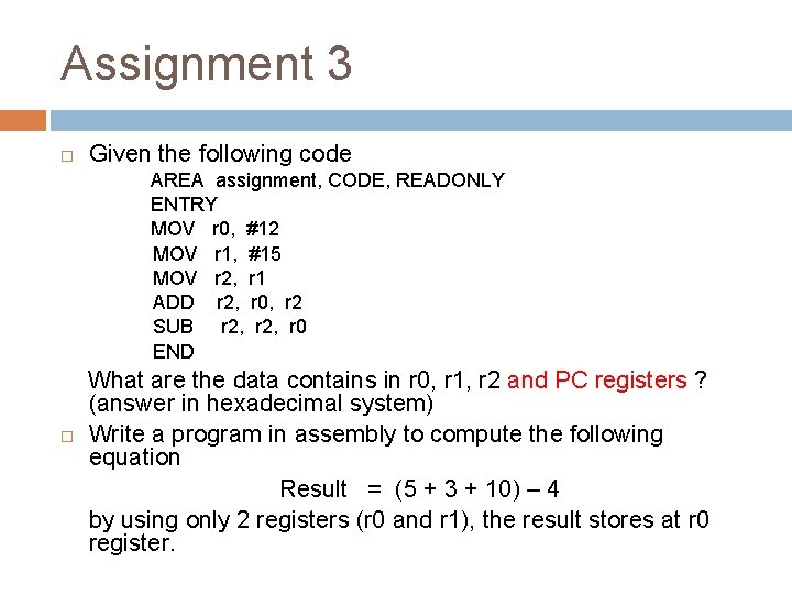
Assignment 3 Given the following code AREA assignment, CODE, READONLY ENTRY MOV r 0, #12 MOV r 1, #15 MOV r 2, r 1 ADD r 2, r 0, r 2 SUB r 2, r 0 END What are the data contains in r 0, r 1, r 2 and PC registers ? (answer in hexadecimal system) Write a program in assembly to compute the following equation Result = (5 + 3 + 10) – 4 by using only 2 registers (r 0 and r 1), the result stores at r 0 register.