Introduction to Electronic Design Automation CADET Week 1
- Slides: 36
Introduction to Electronic Design Automation 北京航空航天大学微电子学院 CADET实验室 成元庆 主讲
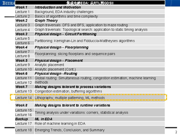
Week 1 Lecture 2 Week 2 Lecture 3 Lecture 4 Week 3 Lecture 5 Lecture 6 Week 4 Lecture 7 Lecture 8 Week 5 Lecture 9 Lecture 10 Week 6 Lecture 11 Lecture 12 Week 7 Lecture 13 集成电路EDA: 从RTL到GDSII Introduction and Motivation Background, EDA industry challenges Basics of algorithms and time complexity Graph Theory Graph traversals: DFS and BFS, application to maze routing Graph traversals: Topological search: application to static timing analysis Physical design – Circuit Partitioning: Kernighan-Lin and Fidduccia-Mattheyses algorithms Physical design – Floorplanning: slicing floorplans and sequence pairs Physical design – Placement Analytic placement (Cont. ) Physical design –Routing Global routing: Simultaneous routing, congestion estimation, machine learning methods Making designs tolerant to process variations Congestion estimation, buffering algorithms Lecture 14 Lithography, multiple patterning, ML methods Week 8 Lecture 15 Lecture 16 Backup Lecture 17 Making designs tolerant to runtime variations Timing analysis under variations: corners, statistical analysis ML in EDA Role of machine learning in EDA Lecture 18 Emerging Trends, Conclusion, and Summary 2
Manufacturing Variations and their Impact
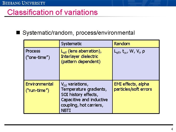
Classification of variations n Systematic/random, process/environmental Systematic Random Process (“one-time”) Leff (lens aberration), Interlayer dielectric (pattern dependent) Leff, tox, W, Vt, ρ Environmental (“run-time”) Vdd variations, Temperature gradients, SOI history effects, Capacitive and inductive coupling, hot carriers, NBTI EMI effects, alpha particles/soft errors 4
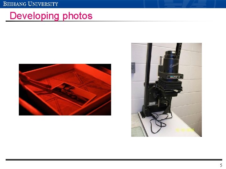
Developing photos 5
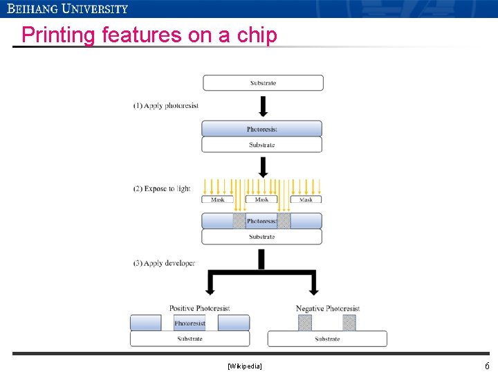
Printing features on a chip [Wikipedia] 6
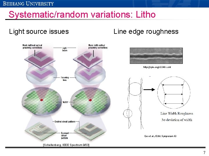
Systematic/random variations: Litho Light source issues Line edge roughness http: //spie. org/x 32401. xml Cao et al. , EUVL Symposium 02 [Schellenberg, IEEE Spectrum 9/03] 7
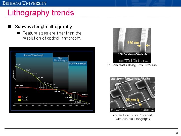
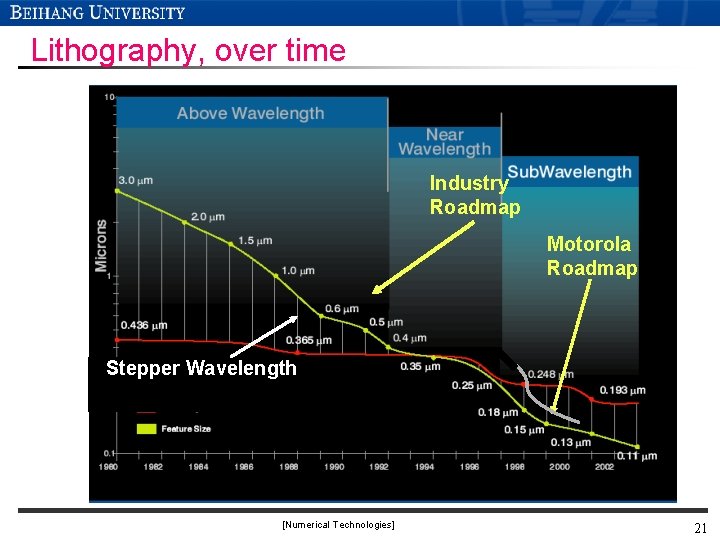
Lithography trends n Subwavelength lithography n Feature sizes are finer than the resolution of optical lithography 8
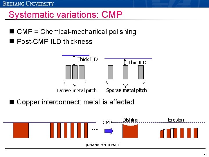
Systematic variations: CMP n CMP = Chemical-mechanical polishing n Post-CMP ILD thickness Thick ILD Dense metal pitch Thin ILD Sparse metal pitch n Copper interconnect: metal is affected … CMP Dishing Erosion [Mehtrotra et al. , IEDM 98] 9
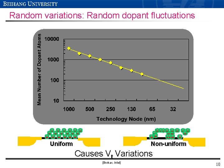
Random variations: Random dopant fluctuations Uniform Non-uniform Causes Vt Variations [Borkar, Intel] 10
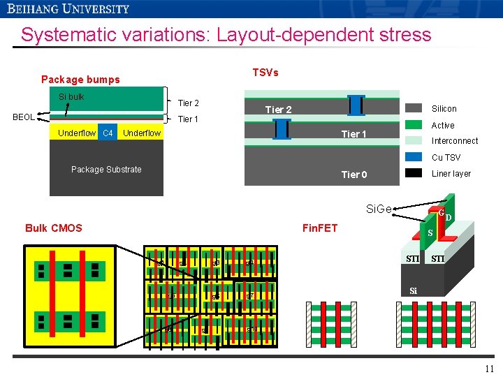
Systematic variations: Layout-dependent stress TSVs Package bumps Si bulk Tier 2 BEOL Tier 1 Underflow C 4 Silicon Tier 2 Underflow Active Tier 1 Interconnect Cu TSV Package Substrate Liner layer Tier 0 Si. Ge Bulk CMOS G Fin. FET g 1 g 2 g 5 g 8 g 9 D S g 3 g 4 STI g 6 g 7 Si STI g 10 11
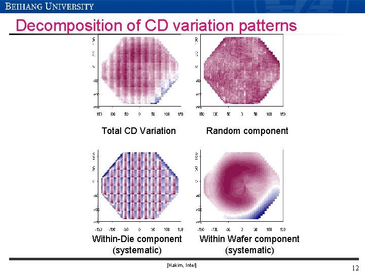
Decomposition of CD variation patterns Total CD Variation Random component Within-Die component (systematic) Within Wafer component (systematic) [Hakim, Intel] 12
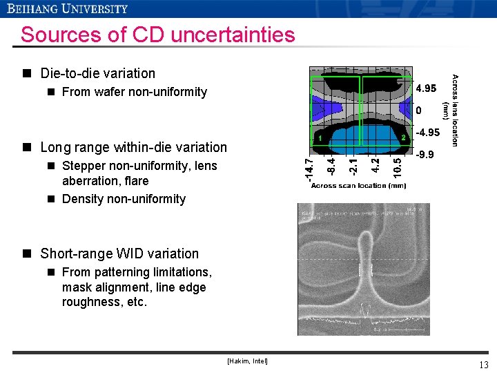
Sources of CD uncertainties n Die-to-die variation n From wafer non-uniformity n Long range within-die variation n Stepper non-uniformity, lens aberration, flare n Density non-uniformity n Short-range WID variation n From patterning limitations, mask alignment, line edge roughness, etc. [Hakim, Intel] 13
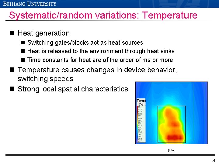
Systematic/random variations: Temperature n Heat generation n Switching gates/blocks act as heat sources n Heat is released to the environment through heat sinks n Time constants for heat are of the order of ms or more n Temperature causes changes in device behavior, switching speeds n Strong local spatial characteristics [Intel] 14
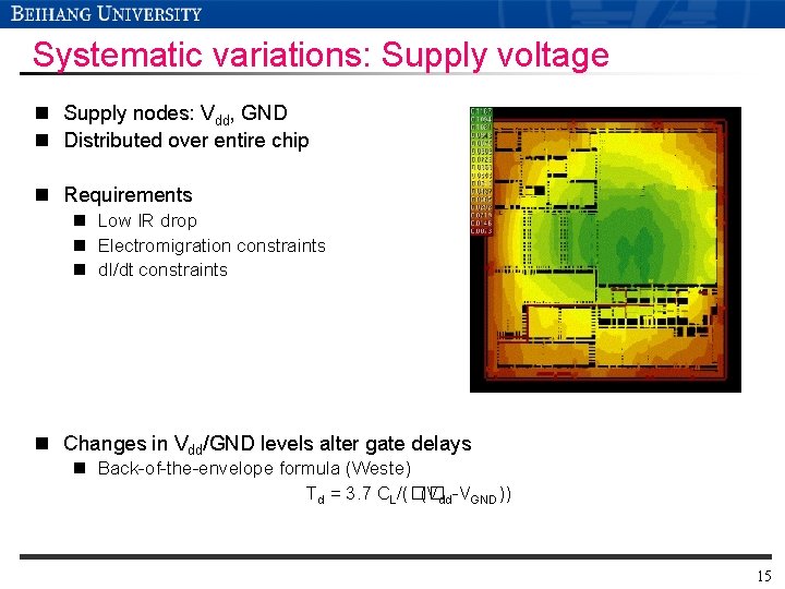
Systematic variations: Supply voltage n Supply nodes: Vdd, GND n Distributed over entire chip n Requirements n Low IR drop n Electromigration constraints n d. I/dt constraints n Changes in Vdd/GND levels alter gate delays n Back-of-the-envelope formula (Weste) Td = 3. 7 CL/(�� (Vdd-VGND)) 15
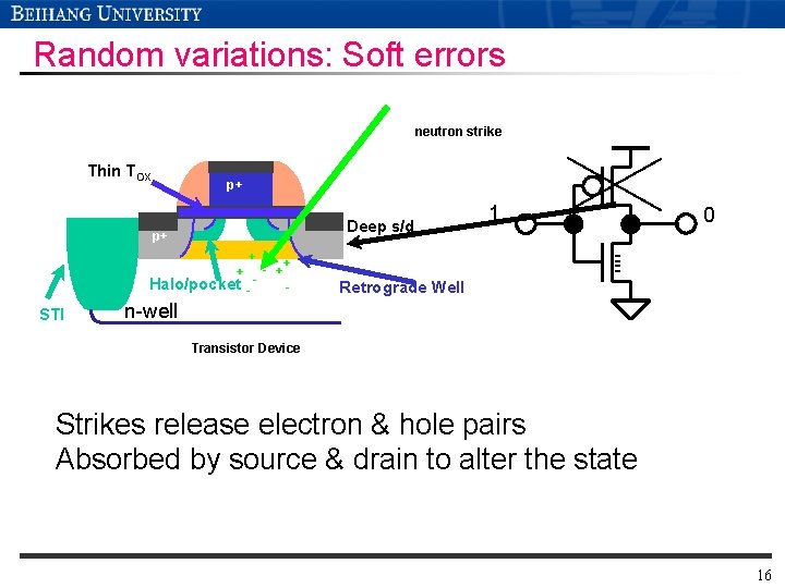
Random variations: Soft errors neutron strike Thin TOX p+ Deep s/d p+ + + Halo/pocket STI - ++ - Retrograde Well 1 0 --- n-well Transistor Device Strikes release electron & hole pairs Absorbed by source & drain to alter the state 16
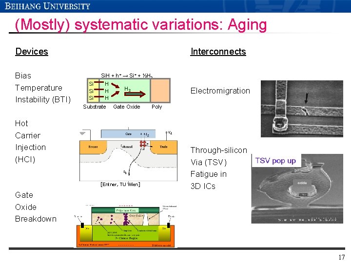
(Mostly) systematic variations: Aging Devices Bias Temperature Instability (BTI) Interconnects Si. H + h+ → Si+ + ½H 2 Si Si Si H H H Substrate H 2 Gate Oxide Hot Carrier Injection (HCI) [Entner, TU Wien] Gate Oxide Breakdown Electromigration Poly Through-silicon Via (TSV) Fatigue in 3 D ICs 17
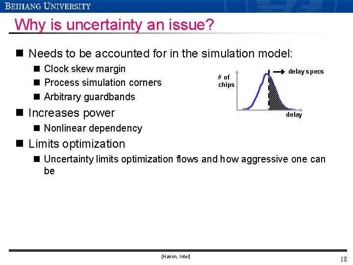
Why is uncertainty an issue? n Needs to be accounted for in the simulation model: n Clock skew margin n Process simulation corners n Arbitrary guardbands n Increases power # of chips delay specs delay n Nonlinear dependency n Limits optimization n Uncertainty limits optimization flows and how aggressive one can be [Hakim, Intel] 18
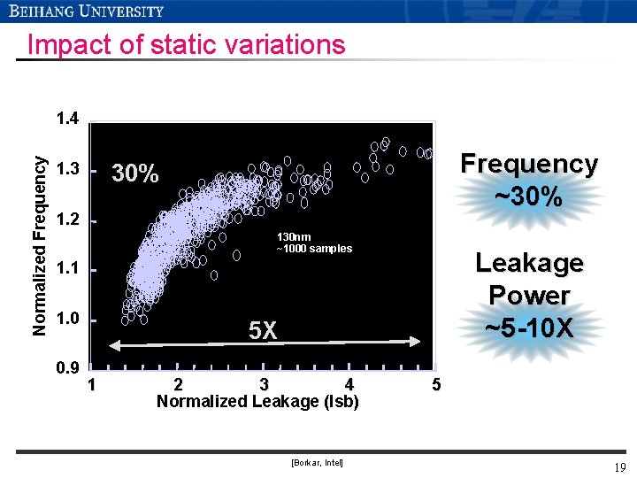
Impact of static variations Normalized Frequency 1. 4 1. 3 Frequency ~30% 1. 2 130 nm ~1000 samples Leakage Power ~5 -10 X 1. 1 1. 0 0. 9 5 X 1 2 3 4 Normalized Leakage (Isb) [Borkar, Intel] 5 19
Lithography
Lithography, over time Industry Roadmap Motorola Roadmap Stepper Wavelength [Numerical Technologies] 21
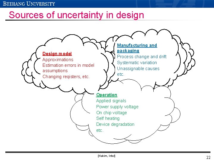
Sources of uncertainty in design Manufacturing and packaging Process change and drift Systematic variation Unassignable causes etc. Design model Approximations Estimation errors in model assumptions Changing reqisters, etc. Operation Applied signals Power supply voltage On chip voltage Self heating Device degradation etc. [Hakim, Intel] 22
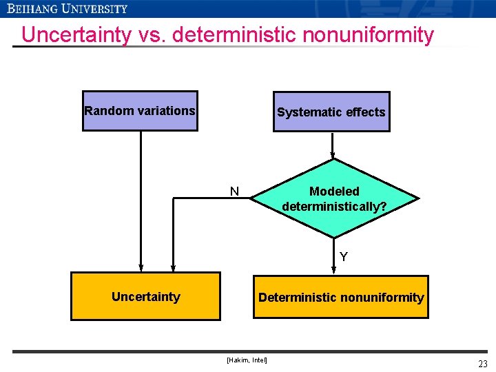
Uncertainty vs. deterministic nonuniformity Random variations Systematic effects Modeled deterministically? N Y Uncertainty Deterministic nonuniformity [Hakim, Intel] 23
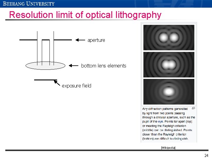
Resolution limit of optical lithography aperture bottom lens elements exposure field [Wikipedia] 24
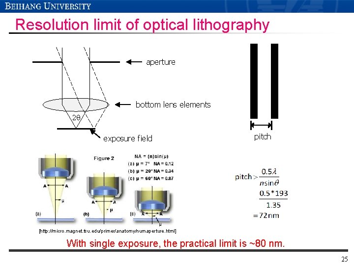
Resolution limit of optical lithography aperture bottom lens elements 2 q exposure field pitch [http: //micro. magnet. fsu. edu/primer/anatomy/numaperture. html] With single exposure, the practical limit is ~80 nm. 25
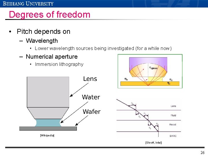
Degrees of freedom • Pitch depends on – Wavelength • Lower wavelength sources being investigated (for a while now) – Numerical aperture • Immersion lithography [Wikipedia] [Shroff, Intel] 26
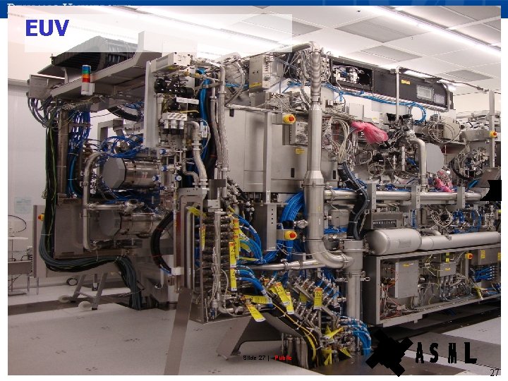
EUV Slide 27 | Public 27
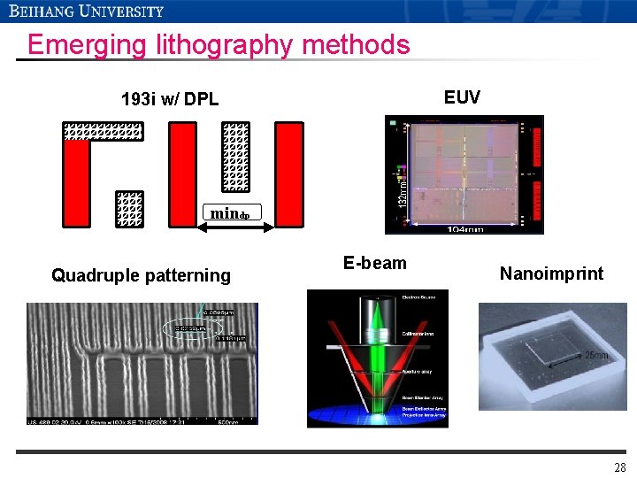
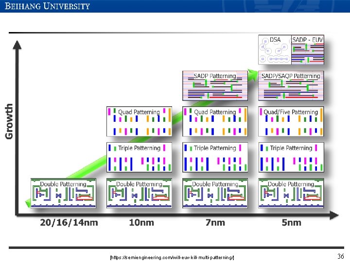
Emerging lithography methods EUV 193 i w/ DPL mindp Quadruple patterning E-beam Nanoimprint 28
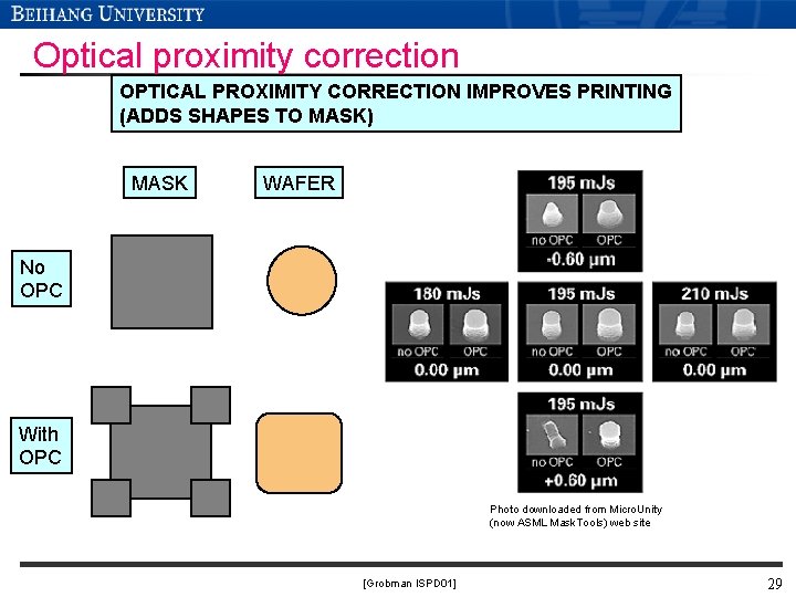
Optical proximity correction OPTICAL PROXIMITY CORRECTION IMPROVES PRINTING (ADDS SHAPES TO MASK) MASK WAFER No OPC With OPC Photo downloaded from Micro. Unity (now ASML Mask. Tools) web site [Grobman ISPD 01] 29
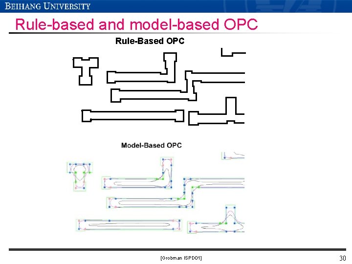
Rule-based and model-based OPC Rule-Based OPC [Grobman ISPD 01] 30
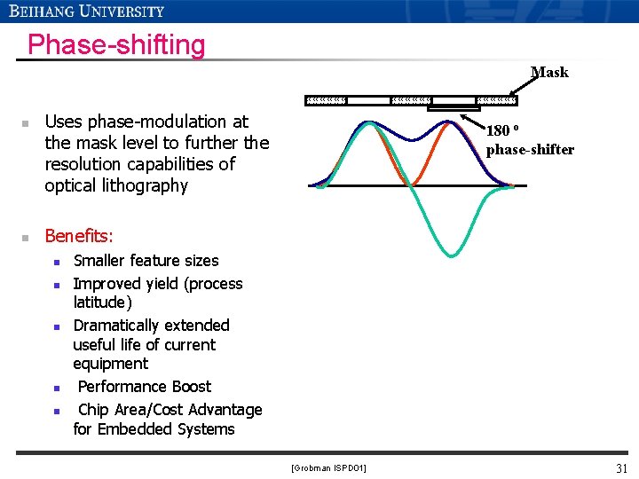
Phase-shifting Mask n n Uses phase-modulation at the mask level to further the resolution capabilities of optical lithography 180 o phase-shifter Benefits: n n n Smaller feature sizes Improved yield (process latitude) Dramatically extended useful life of current equipment Performance Boost Chip Area/Cost Advantage for Embedded Systems [Grobman ISPD 01] 31
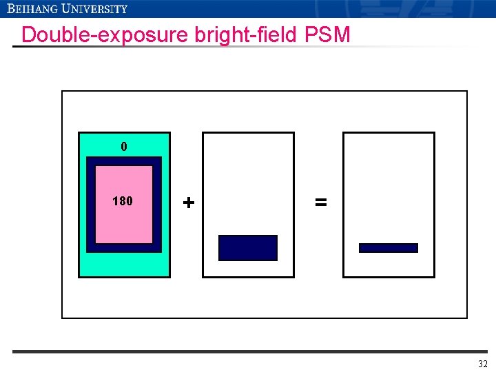
Double-exposure bright-field PSM 0 18 180 0 + = 32
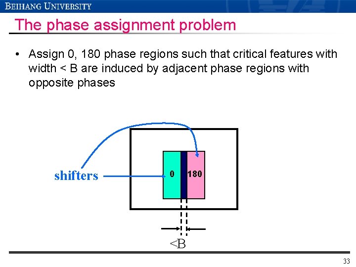
The phase assignment problem • Assign 0, 180 phase regions such that critical features with width < B are induced by adjacent phase regions with opposite phases shifters 0 180 <B 33
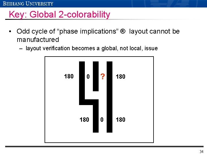
Key: Global 2 -colorability • Odd cycle of “phase implications” ® layout cannot be manufactured – layout verification becomes a global, not local, issue 180 0 ? 180 0 180 34
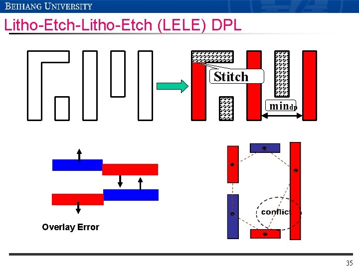
Litho-Etch-Litho-Etch (LELE) DPL A E Stitch mindp Overlay Error 35
[https: //semiengineering. com/will-euv-kill-multi-patterning/] 36