Introduction to Clock Tree Synthesis Clock Jargon Important

 is")


? It is a process to ensure that clock")

")
")


:")
")


- Slides: 58
Introduction to Clock Tree Synthesis
Clock Jargon : Important Terms Clock to an SOC (System on a Chip) is like blood to a human body. Just the way blood flows to each and every part of the human body and regulates metabolism, clock reached each and every sequential device and controls the digital events inside an SOC. Clock Latency: Delay the clock signal takes between any two points. It can be from the source (PLL) to the source pin (Clock pin) of registers. Source Insertion Delay: This is the clock delay from the clock origin point, which could be PLL to the clock definition point. Network Insertion Delay: This refers to the clock delay from the clock definition point to the sink pink of the registers.
Representation of Clock based delays in clock path
Clock Skew:
The Clock Design Problem:
Uneven spread of flops on a chip:
Clock Tree:
Clock Trees:
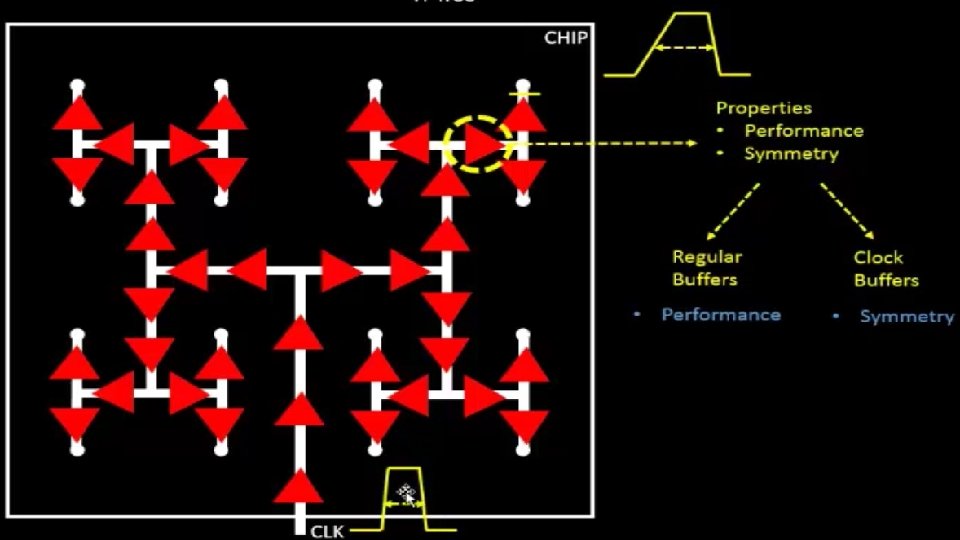
What is Clock Tree Synthesis (CTS)? It is a process to ensure that clock gets distributed evenly to all sequential elements in a design. CTS is the design step to form clock tree distribution. Goal of the CTS is to minimize clock latency and skew. It is the step where the actual clock tree is synthesized. Before CTS timing tools use ideal clock arrival times. After CTS real clock distribution is available, therefore real clock arrival times are used.
CTS Quality Check- I:
False Data Capture (late clock/clock skew)
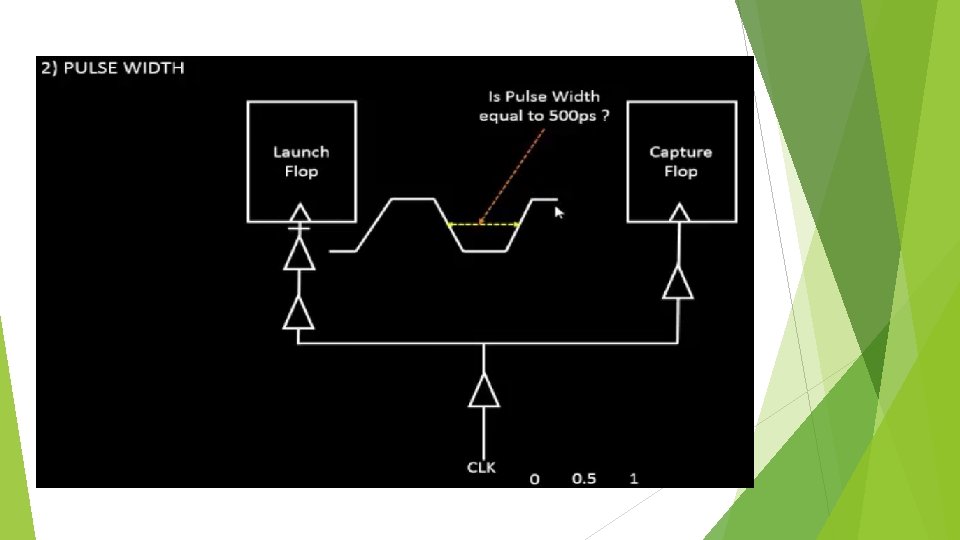
CTS Quality Check – II (Maintain PW of 1 ns)
CTS Quality Check -III
CTS Quality Check - IV
CTS Quality Check - V
CTS Quality Check –VI
Skew generated due to close proximity of nets
Crosstalk might lead to a functional failure:
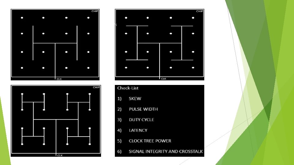
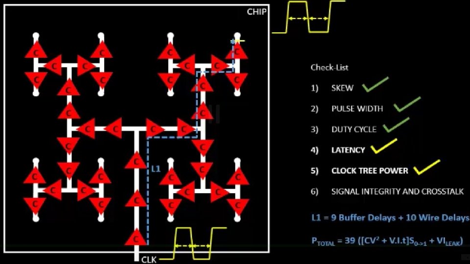
CTS Check List: SKEW PULSE WIDTH DUTY CYCLE LATENCY CLOCK TREE POWER SIGNAL INTEGRITY AND CROSS-TALK
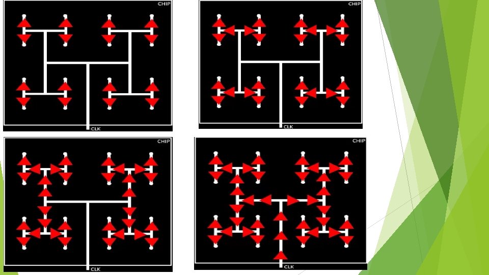
H-Tree Algorithm Goal : The clock reaches each and every flop end point and fulfills all the quality check parameters as discussed. It works on divide and conquer approach. Divide the chip into equal parts.
Implemented H-Tree Quality Parameter Check : Skew
Modeling the RC Network Delay on a chip:
Degradation of Pulse Width due to RC Network
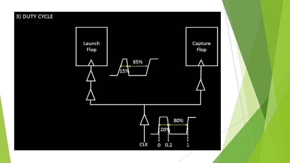
Pulse Width degradation kills performance: Duty Cycle Check is a more comprehensive Pulse Width check.
Implemented H-Tree Parameter check: Latency The clock input and output transition waveforms are way off. We need to optimize the RC network delays by reducing the RC stages to improve latency.
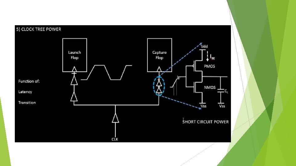
Implemented H-Tree Parameter Check : Power Clock Tree Power dissipation is a function of latency and the output transition. Clock signal continuously running from start to end without any breaks or help (Analogy: Athlete’s race). Energy consumed is humongous.
The bigger picture of the problem:
Clock Tree Modeling: Anything having a physical dimension has a finite resistance and capacitance. Clock end points are connected to flip flops which are load Capacitance(CL). This whole wire model can be represented as a lumped RC model. The clock port has a resistance Rd or the driver resistance.
The simplified RC Model:
Dependence of Time Constant on Length:
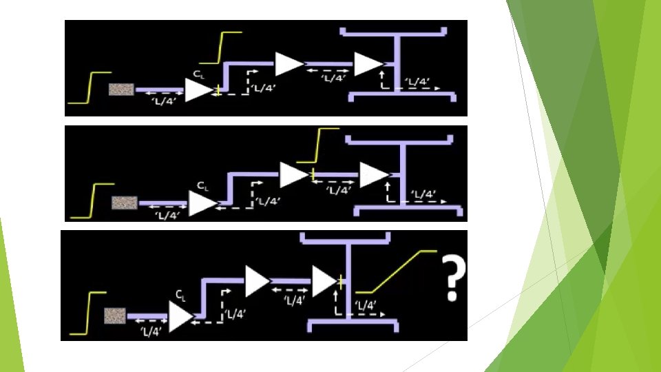
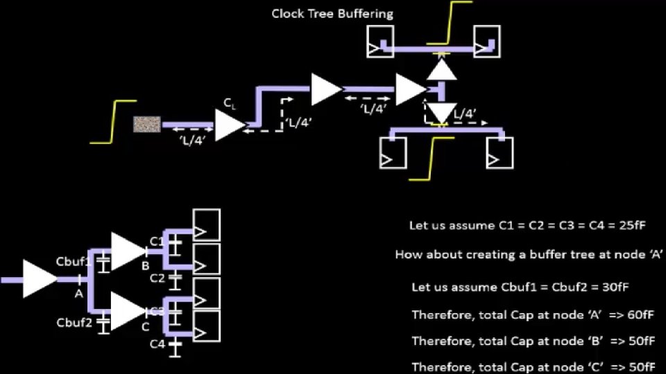
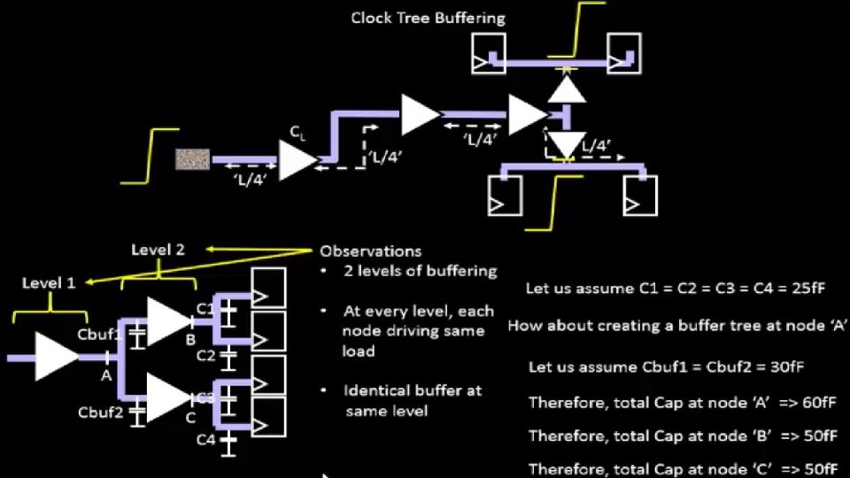
Clock Tree Buffering: Initially the entire Load Capacitance of wire was on the flop, leading to poor output transitions.
Quantifying the no. of buffers added
Buffer implementation despite few drawbacks: Buffer adds to the area cost, imagine area consumed if few buffers are added on each of the million clock paths on a chip. Load on the buffer is twice than the max capacity of decent operation. How about building a buffer tree at node A? (Analogy: Man pushing 4 blocks alone)
Critical conditions to be satisfied for a satisfactory clock tree built:
Validating the design conditions to be met:
Validating the Quality check parameters (Skew):
Quality Check parameter for H-Tree (PW)
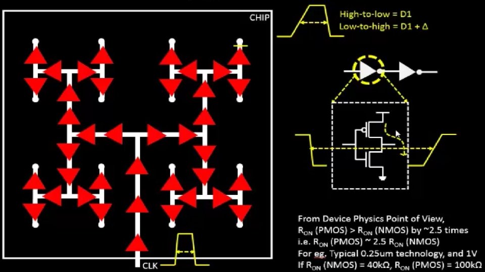
Why Skew test passed and not the PW check? The level of buffering and load driven by each buffer being the same, results in a successful minimal (~0) skew. The output transition is better with the H- Tree as compared to previous results but the rise transition is greater than the fall transition at the output. This results in Pulse Width increase (Time period) and decrease of frequency. Further analysis of the buffer is required to get to our solution. The buffer used in the data path is not the same as the ones used in the clock path. Choice of clock buffers is a tradeoff between the performance and symmetry.
Examining unequal rise and fall times in PW check:
More resistive PMOS allows less current to pass:
Manipulating the size of the PMOS to achieve equal rise, fall times but leakage power(Clock Buffer):
Analyzing quality checks with clock buffers:
Power check as a function of latency:
Dynamic Power Issue: At every switch you consume a finite amount of power. Charging, discharging of capacitance can be related to filling and emptying water buckets. At any time instant all buffers are consuming power (this is small design).
Short Circuit Power: At an intermediate value of input both PMOS and NMOS are on, leading to a common path to ground and short circuit current flows through it.
Leakage Power: When Vgs > Vt, current flows from Source to Drain and Transistor is ON. Even when Vgs < Vt, small current flows called leakage current (steady state).