Epitaxial Growth An Introduction Mark Hopkinson University of

- Slides: 62

Epitaxial Growth- An Introduction Mark Hopkinson University of Sheffield(UK)

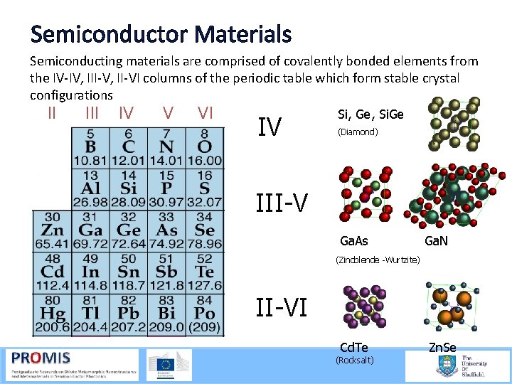
Semiconductor Materials Semiconducting materials are comprised of covalently bonded elements from the IV IV, III V, II VI columns of the periodic table which form stable crystal configurations II IV V VI IV Si, Ge, Si. Ge (Diamond) III-V Ga. As Ga. N (Zincblende -Wurtzite) II-VI Cd. Te (Rocksalt) Zn. Se

So how do we produce these semiconductor materials? The simplest method is bulk crystal growth We take bulk elements and heat them under pressure until the liquid reaches supersaturation Then the introduction of a ‘seed’ crystal initiates the build up of new crystalline material

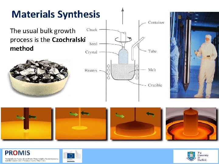
Materials Synthesis The usual bulk growth process is the Czochralski method

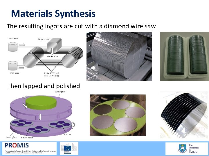
Materials Synthesis The resulting ingots are cut with a diamond wire saw Then lapped and polished

Problems with this approach Thermodymically impossible to produce many compound substrates using this approach Many compounds have a highly reactivity at high temperature We only produce single elements and compounds there is much to be gained by combining semiconductors in heterostructures For this we need an additive (epitaxial) growth approach

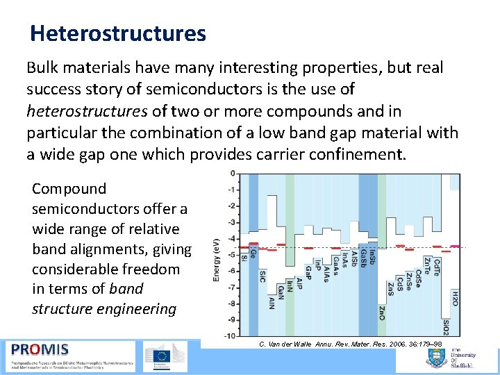
Heterostructures Bulk materials have many interesting properties, but real success story of semiconductors is the use of heterostructures of two or more compounds and in particular the combination of a low band gap material with a wide gap one which provides carrier confinement. Compound semiconductors offer a wide range of relative band alignments, giving considerable freedom in terms of band structure engineering C. Van der Walle Annu. Rev. Mater. Res. 2006. 36: 179– 98

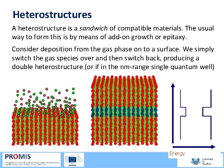
Heterostructures A heterostructure is a sandwich of compatible materials. The usual way to form this is by means of add on growth or epitaxy. Consider deposition from the gas phase on to a surface. We simply switch the gas species over and then switch back, producing a double heterostructure (or if in the nm range single quantum well) Energy

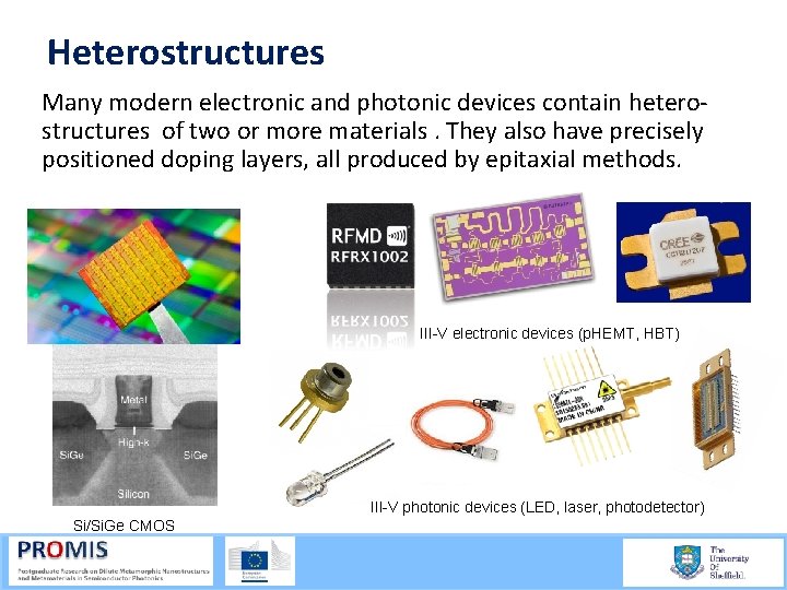
Heterostructures Many modern electronic and photonic devices contain hetero structures of two or more materials. They also have precisely positioned doping layers, all produced by epitaxial methods. III-V electronic devices (p. HEMT, HBT) III-V photonic devices (LED, laser, photodetector) Si/Si. Ge CMOS

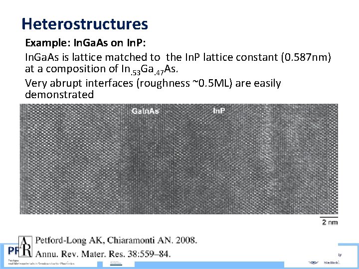
Heterostructures Example: In. Ga. As on In. P: In. Ga. As is lattice matched to the In. P lattice constant (0. 587 nm) at a composition of In. 53 Ga. 47 As. Very abrupt interfaces (roughness ~0. 5 ML) are easily demonstrated

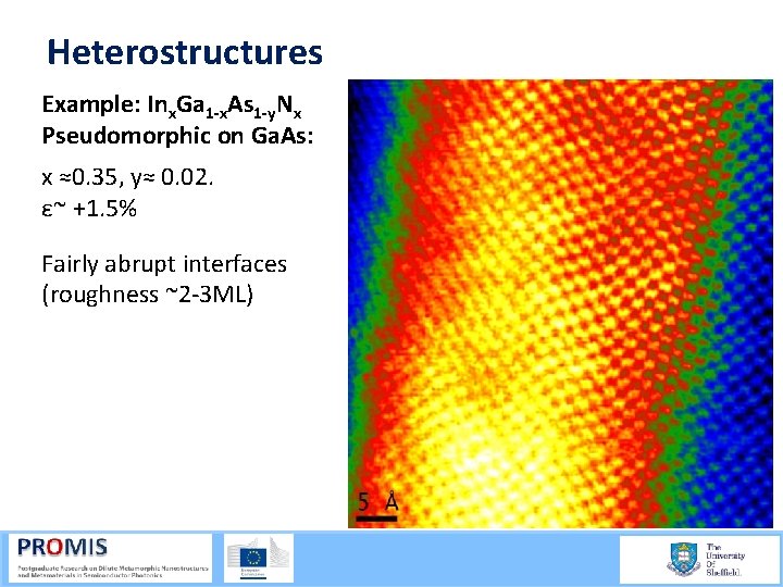
Heterostructures Example: Inx. Ga 1 -x. As 1 -y. Nx Pseudomorphic on Ga. As: x ≈0. 35, y≈ 0. 02. ε~ +1. 5% Fairly abrupt interfaces (roughness ~2 3 ML)

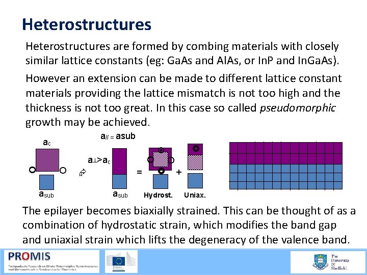
Heterostructures are formed by combing materials with closely similar lattice constants (eg: Ga. As and Al. As, or In. P and In. Ga. As). However an extension can be made to different lattice constant materials providing the lattice mismatch is not too high and the thickness is not too great. In this case so called pseudomorphic growth may be achieved. a// = asub ac a┴>ac asub = asub Hydrost. + Uniax. The epilayer becomes biaxially strained. This can be thought of as a combination of hydrostatic strain, which modifies the band gap and uniaxial strain which lifts the degeneracy of the valence band.

Heterostructures However if the strain thickness product is too high we will induce relaxation in the structure. There are three basic types: Plastic relaxation- introduction of crystal defects Elastic relaxation- deformation of the surface Composition relaxation- promotion of phase separation Plastic Relaxation → Crystal defects (dislocations, twins, stacking faults). These play a major role in device degradation. e. g: in electronic devices, a space charge region exists around a dislocation which scatters carriers & traps carriers. In optical devices dislocations introduce states in the gap, acting as non radiative recombination centres.

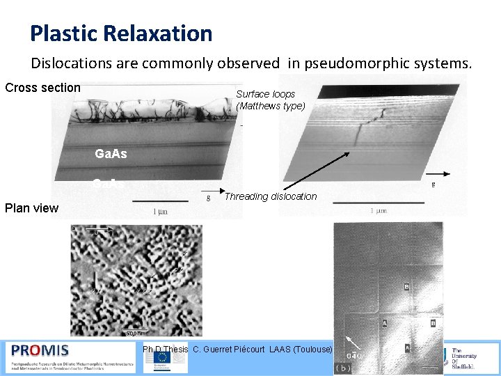
Plastic Relaxation Dislocations are commonly observed in pseudomorphic systems. Cross section Surface loops (Matthews type) Ga. As Plan view Threading dislocation Ph. D Thesis C. Guerret Piécourt LAAS (Toulouse)

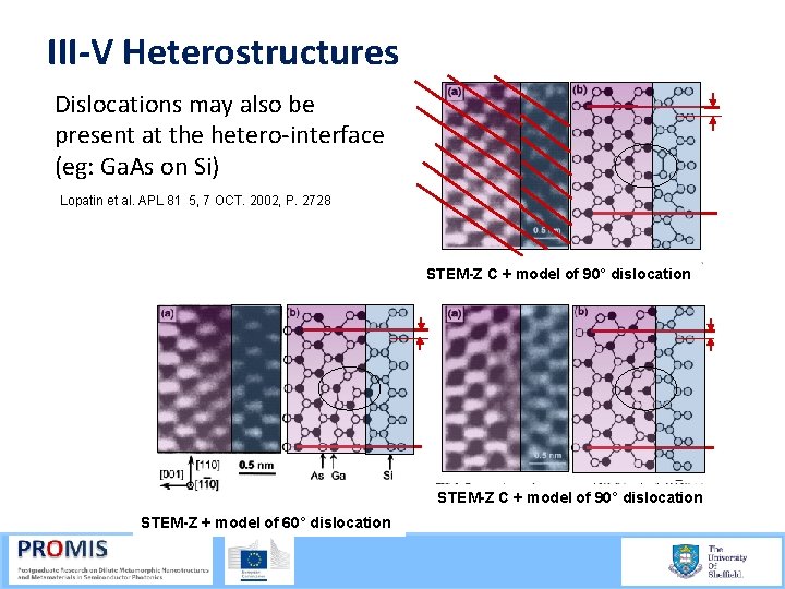
III-V Heterostructures Dislocations may also be present at the hetero interface (eg: Ga. As on Si) Lopatin et al. APL 81 5, 7 OCT. 2002, P. 2728 STEM-Z C + model of 90° dislocation STEM-Z + model of 60° dislocation

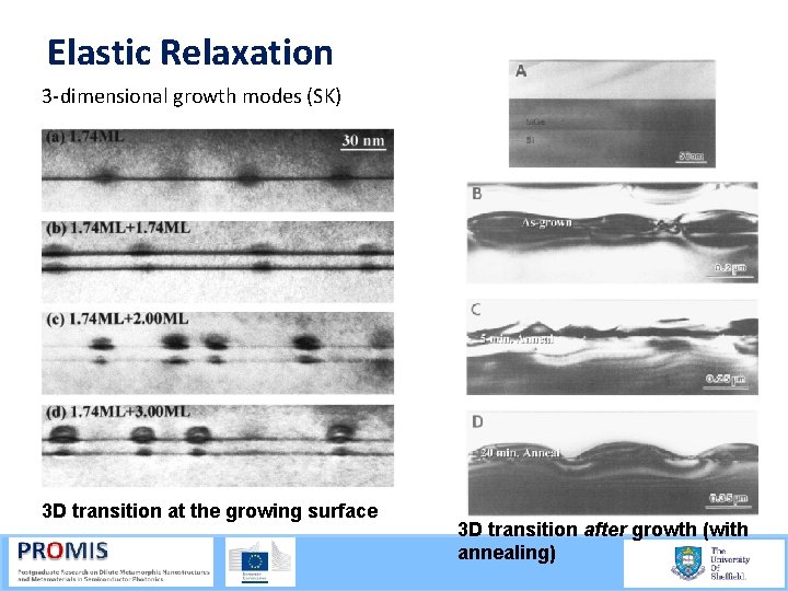
Elastic Relaxation Distortion of a layer by elastic relaxation is much more likely to affect a thin epitaxial layer than bulk materials • Volmer and Weber (1929) observed that crystalline films grow from 3 D nuclei. • Stranski and Krastanov (1938) that a layer could initially grow 2 D up to a critical thickness, beyond which 3 D islands would form and take up their natural lattice constant. • Frank and van der Merve (1949): Identified that monolayer by monolayer growth would always tend to dominate for a layer below a critical misfit level These modes were unified by Bauer (1958) by consideration of the macroscopic free energies.

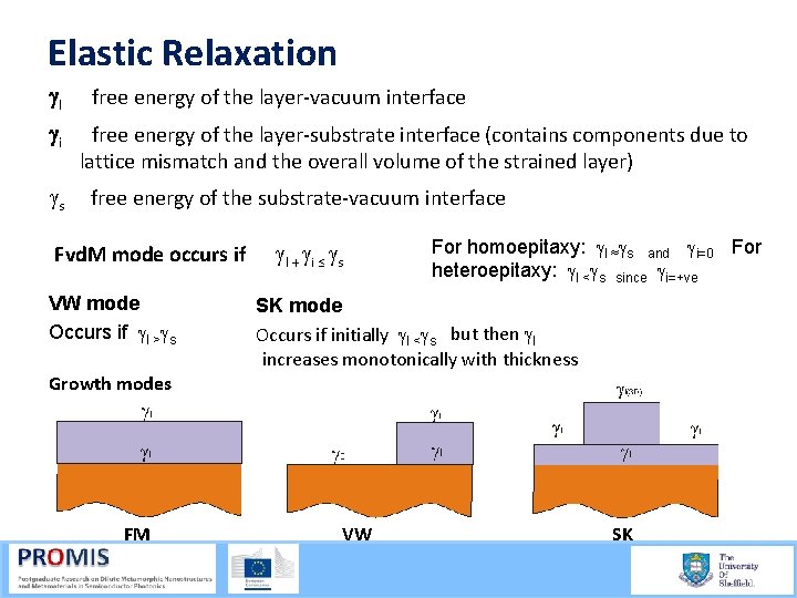
Elastic Relaxation gl gi gs free energy of the layer vacuum interface free energy of the layer substrate interface (contains components due to lattice mismatch and the overall volume of the strained layer) free energy of the substrate vacuum interface Fvd. M mode occurs if VW mode Occurs if gl >gs Growth modes FM gl + gi ≤ gs For homoepitaxy: gl ≈gs and gi=0 For heteroepitaxy: gl <gs since gi=+ve SK mode Occurs if initially gl <gs but then gl increases monotonically with thickness VW SK

Elastic Relaxation 3 dimensional growth modes (SK) 3 D transition at the growing surface 3 D transition after growth (with annealing)

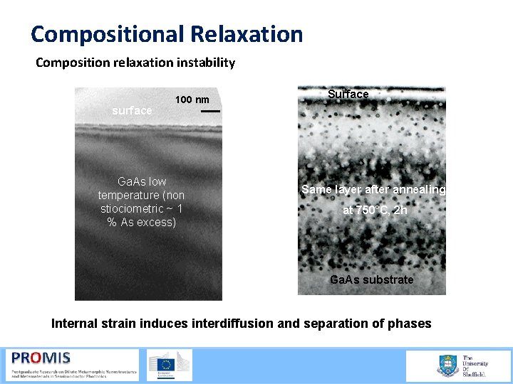
Compositional Relaxation Composition relaxation instability surface 100 nm Ga. As low temperature (non stiociometric ~ 1 % As excess) Surface Same layer after annealing at 750°C, 2 h Ga. As substrate Internal strain induces interdiffusion and separation of phases

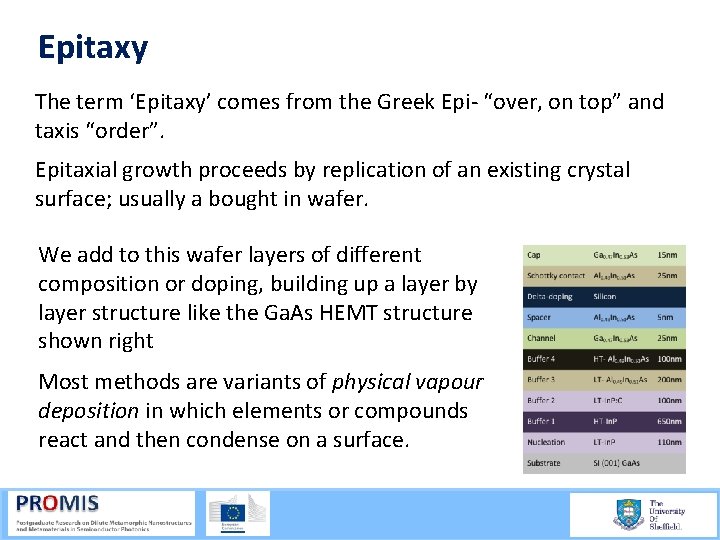
Epitaxy The term ‘Epitaxy’ comes from the Greek Epi “over, on top” and taxis “order”. Epitaxial growth proceeds by replication of an existing crystal surface; usually a bought in wafer. We add to this wafer layers of different composition or doping, building up a layer by layer structure like the Ga. As HEMT structure shown right Most methods are variants of physical vapour deposition in which elements or compounds react and then condense on a surface.

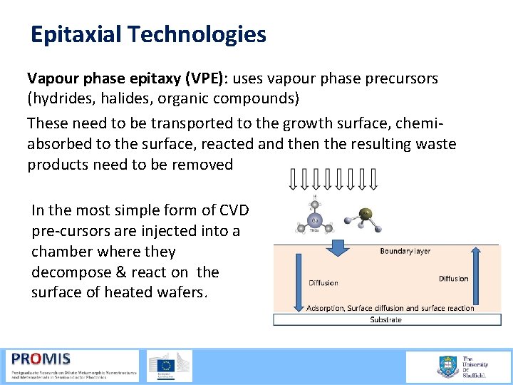
Epitaxial Technologies Vapour phase epitaxy (VPE): uses vapour phase precursors (hydrides, halides, organic compounds) These need to be transported to the growth surface, chemi absorbed to the surface, reacted and then the resulting waste products need to be removed In the most simple form of CVD pre cursors are injected into a chamber where they decompose & react on the surface of heated wafers.

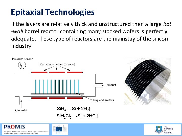
Epitaxial Technologies If the layers are relatively thick and unstructured then a large hot -wall barrel reactor containing many stacked wafers is perfectly adequate. These type of reactors are the mainstay of the silicon industry Si. H 4 →Si + 2 H 2↑ Si. H 2 Cl 2 →Si + 2 HCl↑

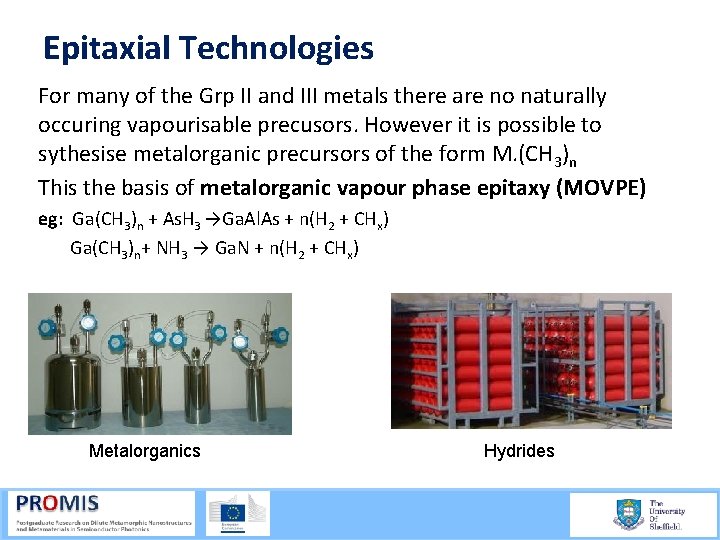
Epitaxial Technologies For many of the Grp II and III metals there are no naturally occuring vapourisable precusors. However it is possible to sythesise metalorganic precursors of the form M. (CH 3)n This the basis of metalorganic vapour phase epitaxy (MOVPE) eg: Ga(CH 3)n + As. H 3 →Ga. Al. As + n(H 2 + CHx) Ga(CH 3)n+ NH 3 → Ga. N + n(H 2 + CHx) Metalorganics Hydrides

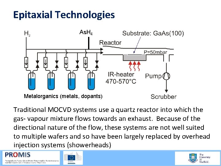
Epitaxial Technologies As. H 4 Metalorganics (metals, dopants) Traditional MOCVD systems use a quartz reactor into which the gas vapour mixture flows towards an exhaust. Because of the directional nature of the flow, these systems are not well suited to multiple wafers and so have been largely replaced by overhead injection systems (showerheads)

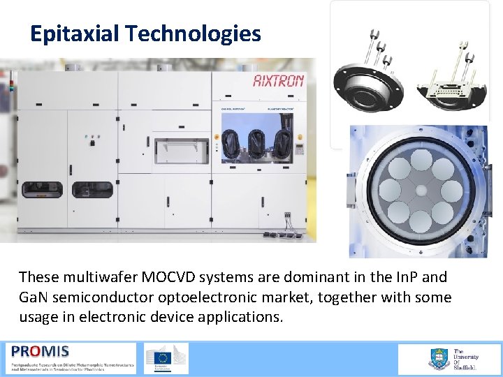
Epitaxial Technologies These multiwafer MOCVD systems are dominant in the In. P and Ga. N semiconductor optoelectronic market, together with some usage in electronic device applications.

Epitaxial Technologies MOVPE has a number of attractive properties. • It is quite easy to refine materials in their gas phase high quality source materials • Easy to handle & switch gas flow mixtures and there are very accurate direct means to measure gas flow rates. • Hydrogen carrier gas provides a strongly reducing environment • Its use of vacuum technology is less demanding than MBE. • It has capabilities for both very low (<nm. s 1) and relatively high (μm. min 1) growth rates • Surface Long diffusion lengths, giving excellent selectivity, ability to change growth modes etc

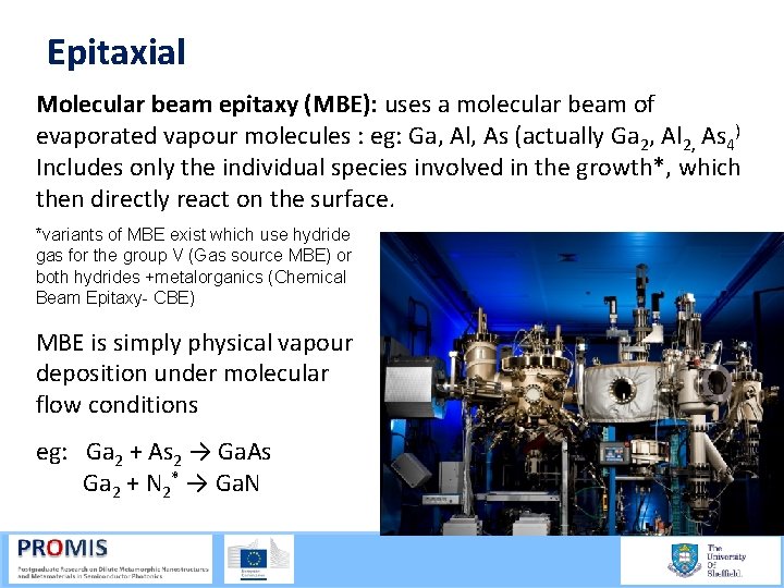
Epitaxial Molecular beam epitaxy (MBE): uses a molecular beam of evaporated vapour molecules : eg: Ga, Al, As (actually Ga 2, Al 2, As 4) Includes only the individual species involved in the growth*, which then directly react on the surface. *variants of MBE exist which use hydride gas for the group V (Gas source MBE) or both hydrides +metalorganics (Chemical Beam Epitaxy- CBE) MBE is simply physical vapour deposition under molecular flow conditions eg: Ga 2 + As 2 → Ga. As Ga 2 + N 2* → Ga. N

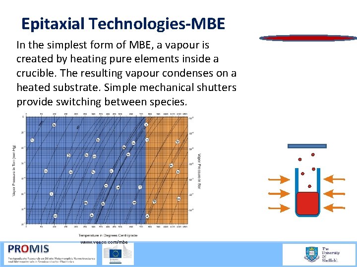
Epitaxial Technologies-MBE In the simplest form of MBE, a vapour is created by heating pure elements inside a crucible. The resulting vapour condenses on a heated substrate. Simple mechanical shutters provide switching between species. www. veeco. com/mbe

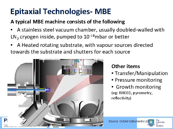
Epitaxial Technologies- MBE A typical MBE machine consists of the following • A stainless steel vacuum chamber, usually doubled walled with LN 2 cryogen inside, pumped to 10 10 mbar or better • A Heated rotating substrate, with vapour sources directed towards the substrate and shutters for each source Other items • Transfer/Manipulation • Pressure monitoring • Growth monitoring (eg: RHEED, pyrometry, reflectivity) Source: Oxford Instruments Ltd

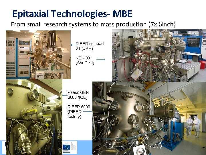
Epitaxial Technologies- MBE From small research systems to mass production (7 x 6 inch) RIBER compact 21 (UPM) VG V 90 (Sheffield) Veeco GEN 2000 (IQE) RIBER 6000 (RIBER factory)

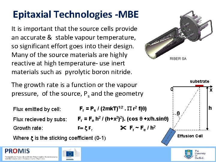
Epitaxial Technologies -MBE It is important that the source cells provide an accurate & stable vapour temperature, so significant effort goes into their design. Many of the source materials are highly reactive at high temperature use inert materials such as pyrolytic boron nitride. The growth rate is a function or the vapour pressure, of the source, Ps and the geometry Flux emitted by cell: Fr = Ps / (2 mk. T)1/2. P r 2 f(q) Flux recieved by subs: Fr = Fe h 2 / (h+x 2)2). (cos q +x/h. sinq) Growth rate: F= x Fr Where x is the sticking coefficient (0 -1) RIBER SA substrate x 0 q Fr ~ F e / h 2 Effusion Cell h

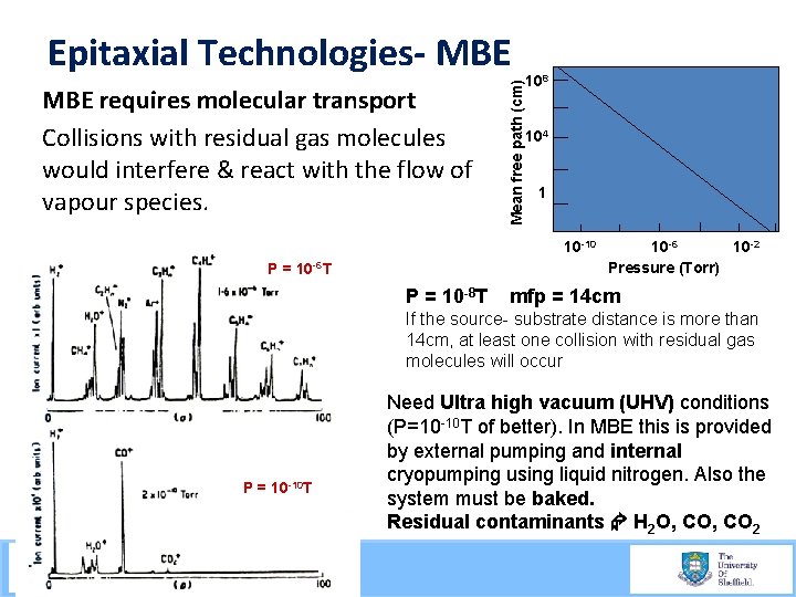
MBE requires molecular transport Collisions with residual gas molecules would interfere & react with the flow of vapour species. Mean free path (cm) Epitaxial Technologies- MBE 108 104 1 10 -10 P = 10 -6 T 300 K P = 10 -8 T 10 -6 10 -2 Pressure (Torr) mfp = 14 cm If the source- substrate distance is more than 14 cm, at least one collision with residual gas molecules will occur P = 10 -10 T Need Ultra high vacuum (UHV) conditions (P=10 -10 T of better). In MBE this is provided by external pumping and internal cryopumping using liquid nitrogen. Also the system must be baked. Residual contaminants H 2 O, CO 2

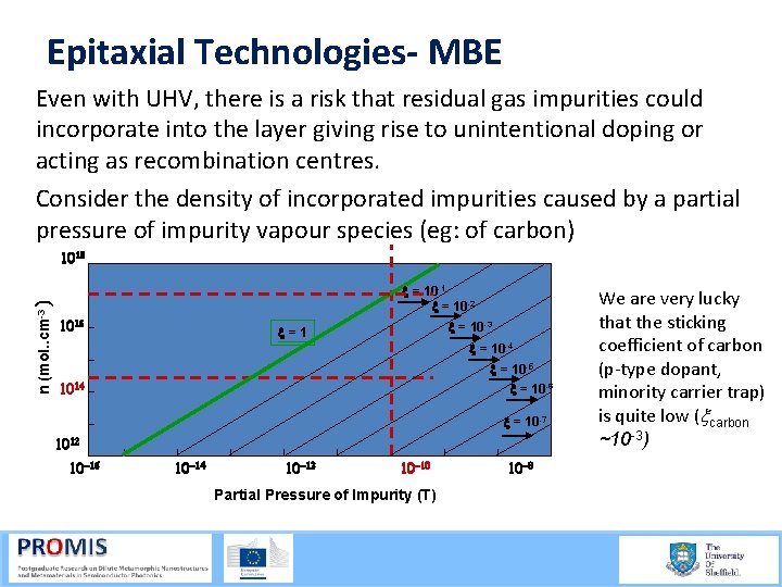
Epitaxial Technologies- MBE Even with UHV, there is a risk that residual gas impurities could incorporate into the layer giving rise to unintentional doping or acting as recombination centres. Consider the density of incorporated impurities caused by a partial pressure of impurity vapour species (eg: of carbon) n (mol. . cm-3 ) 1018 x = 10 -1 x = 10 -2 1016 x = 10 -3 x=1 x = 10 -4 x = 10 -5 x = 10 -6 1014 x = 10 -7 1012 10 -16 10 -14 10 -12 10 -10 Partial Pressure of Impurity (T) 10 -8 We are very lucky that the sticking coefficient of carbon (p type dopant, minority carrier trap) is quite low (xcarbon ~10 -3)

Epitaxial Technologies- MBE Achieving and retaining UHV is of critical importance in MBE and this all adds to the complexity and cost. MBE characteristics • Ultimate in purity (for those who invest the effort and money) • Abrupt switching, coupled with relatively slow growth rates: good for nanostructures • Relatively low growth temperatures: Low thermal budget, Reduced interdiffusion • In situ (in vacuum) diagnosis: Mass spectrometry. Electron diffraction analysis of surfaces (RHEED), Surface spectroscopy etc • Potential to transfer to other vacuum processing tools eg: other semiconductor, metallisation, etching.

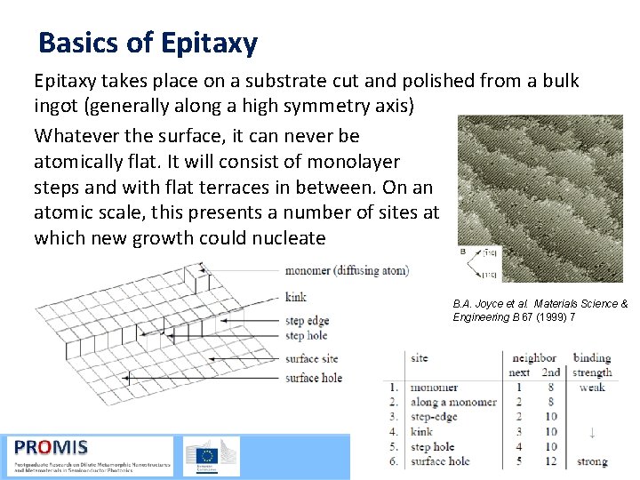
Basics of Epitaxy takes place on a substrate cut and polished from a bulk ingot (generally along a high symmetry axis) Whatever the surface, it can never be atomically flat. It will consist of monolayer steps and with flat terraces in between. On an atomic scale, this presents a number of sites at which new growth could nucleate B. A. Joyce et al. Materials Science & Engineering B 67 (1999) 7

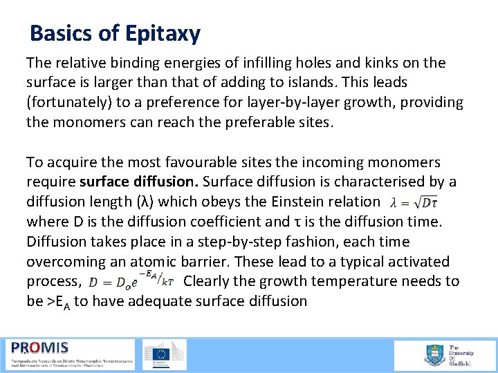
Basics of Epitaxy The relative binding energies of infilling holes and kinks on the surface is larger than that of adding to islands. This leads (fortunately) to a preference for layer by layer growth, providing the monomers can reach the preferable sites. To acquire the most favourable sites the incoming monomers require surface diffusion. Surface diffusion is characterised by a diffusion length (λ) which obeys the Einstein relation where D is the diffusion coefficient and τ is the diffusion time. Diffusion takes place in a step by step fashion, each time overcoming an atomic barrier. These lead to a typical activated process, Clearly the growth temperature needs to be ˃EA to have adequate surface diffusion.

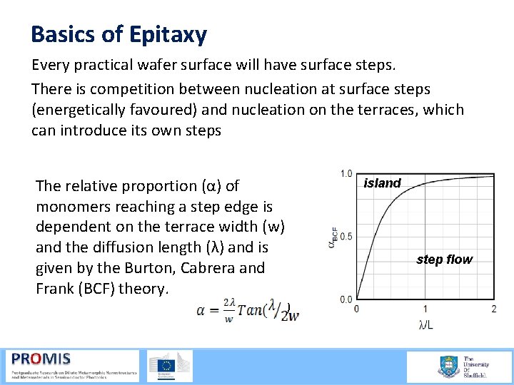
Basics of Epitaxy Every practical wafer surface will have surface steps. There is competition between nucleation at surface steps (energetically favoured) and nucleation on the terraces, which can introduce its own steps The relative proportion (α) of monomers reaching a step edge is dependent on the terrace width (w) and the diffusion length (λ) and is given by the Burton, Cabrera and Frank (BCF) theory. island step flow )

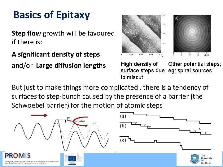
Basics of Epitaxy Step flow growth will be favoured if there is: A significant density of steps and/or Large diffusion lengths High density of Other potential steps; surface steps due eg: spiral sources to miscut But just to make things more complicated , there is a tendency of surfaces to step bunch caused by the presence of a barrier (the Schwoebel barrier) for the motion of atomic steps

Basics of Epitaxy So what is better, step flow or island growth? Ideal step flow always proceeds through the completion of a monolayer before the growth of the next one begins. In this way the crystal surface remains two dimensional in nature and is abrupt to ± 0. 5 ML (~ 0. 15 nm). This is important for the production of high quality two dimensional heterostructures. Growth by island nucleation does not involve the completion of one layer before another one can start. It can therefore be susceptible to roughening and clustering processes. However the roughening processes are self limiting and you can in controlled conditions get good epitaxial growth.

Basics of Epitaxy Chemical potential The energy of bonding is characterised by the chemical potential. Considering Ga. As as an example, according to theories of Gibbs the chemical potential of Ga. As, µGa. As , must be equal to the sum of the free elements , µGa + µAs otherwise the bulk would be unstable to the loss of one of the elements. Also the chemical potential of the free elements must be lower than that of the bulk elements.

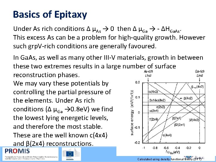
Basics of Epitaxy therefore, µGa < µGa, bulk and µAs < µAs, bulk It is useful to consider the differences in chemical potential from the bulk values, Δ µGa = µGa, bulk < 0 and Δ µAs = µAs , bulk< 0 Considering Ga. As: µGa. As, bulk µGa, bulk µAs, bulk= Δ µGa+ Δ µAs < 0. The first term is simply the energy of formation of Ga. As, ΔHGa. As This is well known to be ≈ 0. 80 e. V per molecule. Two extremes can now exist. If Δ µGa → 0 then Δ µAs → ΔHGa. As. In this situation there is no energy difference between free Ga and Ga in bulk Ga. As. Metallic Ga droplets form on the surface in this Ga rich growth condition.

Basics of Epitaxy Under As rich conditions Δ µAs → 0 then Δ µGa → ΔHGa. As. This excess As can be a problem for high quality growth. However such grp. V rich conditions are generally favoured. In Ga. As, as well as many other III V materials, growth in between these two extremes results in a large number of surface reconstruction phases. We may vary these potentials by controlling the partial pressure of the elements. Under As rich conditions (Δ µGa → 0. 8 e. V) we find the lowest lying energetic levels, and therefore the most stable. These are the well known c(4 x 4) and β(2 x 4) reconstructions. Calculated using density functional theory (DFT)

Basics of Epitaxy Note under As rich conditions, which are typical, one is basically saturating the surface with As. Under this situation it is possible to treat the growth as the adsorption and diffusion of Ga on the surface, with the excess As just ‘waiting’ for the Ga to incorporate. The growth rate is then determined by the Ga flux, with the excess As having a secondary role. Surface Reconstructions The surface of covalent crystals is comprised of unsatisfied dangling bonds. Rather than retain the bulk geometry, the surface atoms are prone to re arrange themselves to lower their surface energy. These are called surface reconstructions.

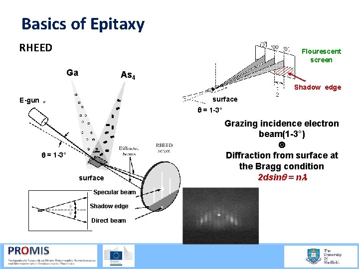
Basics of Epitaxy Surface reconstructions can have significantly different structure of stoiciometry to the bulk. They play an important role in the epitaxy, since incoming monomers are interacting with the surface and not the bulk. The nomenclature of surface reconstructions reflects the symmetry in multiples of the original unit cell basis. For the most common (001) surface reconstructions such as the (2 x 4) reflect a surface unit cell of 2 times Our primary means on observing these is through surface electron diffraction Reflection High Energy Electron diffraction (RHEED). Their effect on the optical anistropy can be also observed in Reflectance Anistropy Spectroscopy (RAS)

Basics of Epitaxy RHEED Flourescent screen Ga As 4 Shadow edge surface E-gun q = 1 -3° surface Specular beam Shadow edge Direct beam Grazing incidence electron beam(1 -3°) Diffraction from surface at the Bragg condition 2 dsinq = nl

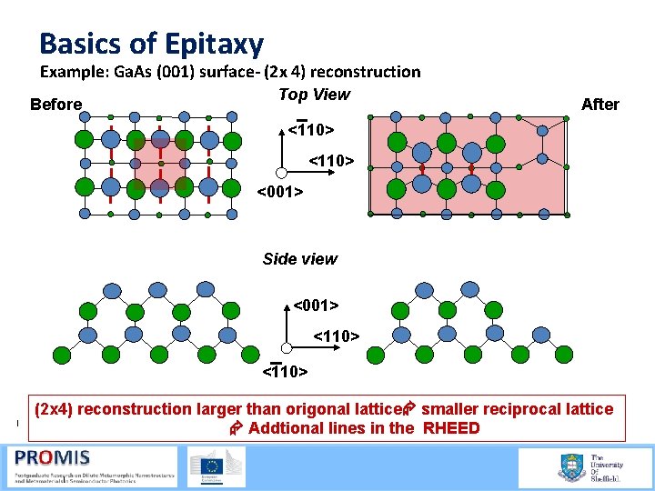
Basics of Epitaxy Example: Ga. As (001) surface- (2 x 4) reconstruction Before Top View After <110> <001> Side view <001> <110> (2 x 4) reconstruction larger than origonal lattice smaller reciprocal lattice Addtional lines in the RHEED

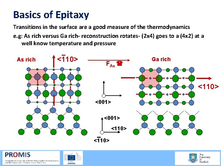
Basics of Epitaxy Transitions in the surface are a good measure of thermodynamics e. g: As rich versus Ga rich- reconstruction rotates- (2 x 4) goes to a (4 x 2) at a well know temperature and pressure As rich <110> FAs Ga rich <110> <001> <110>

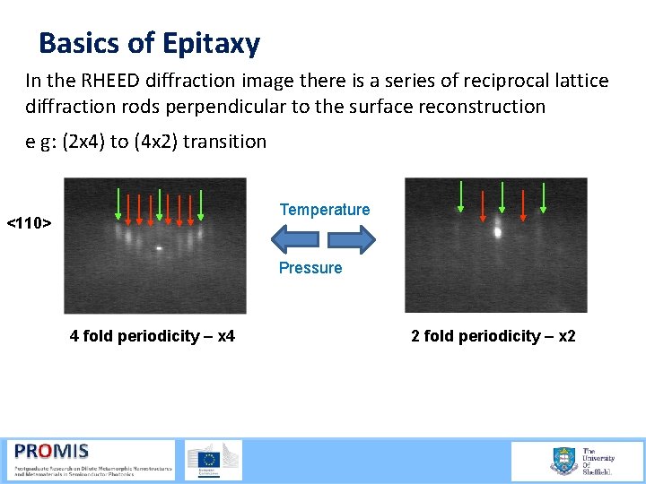
Basics of Epitaxy In the RHEED diffraction image there is a series of reciprocal lattice diffraction rods perpendicular to the surface reconstruction e g: (2 x 4) to (4 x 2) transition Temperature <110> Pressure 4 fold periodicity – x 4 2 fold periodicity – x 2

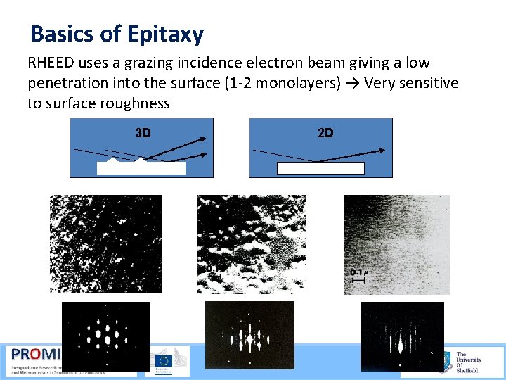
Basics of Epitaxy RHEED uses a grazing incidence electron beam giving a low penetration into the surface (1 2 monolayers) → Very sensitive to surface roughness 3 D 2 D

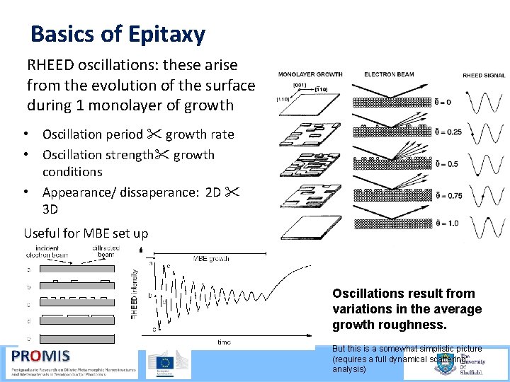
Basics of Epitaxy RHEED oscillations: these arise from the evolution of the surface during 1 monolayer of growth • Oscillation period growth rate • Oscillation strength growth conditions • Appearance/ dissaperance: 2 D 3 D Useful for MBE set up Oscillations result from variations in the average growth roughness. But this is a somewhat simplistic picture (requires a full dynamical scattering analysis)

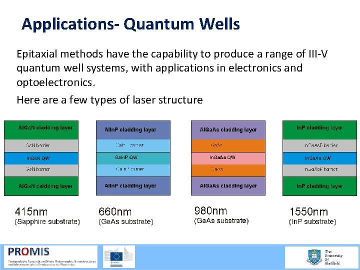
Applications- Quantum Wells Epitaxial methods have the capability to produce a range of III V quantum well systems, with applications in electronics and optoelectronics. Here a few types of laser structure

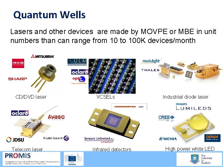
Quantum Wells Lasers and other devices are made by MOVPE or MBE in unit numbers than can range from 10 to 100 K devices/month CD/DVD laser Telecom laser VCSELs Infrared detectors Industrial diode laser High power white LED

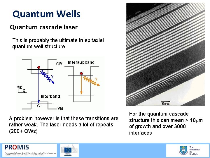
Quantum Wells Quantum cascade laser This is probably the ultimate in epitaxial quantum well structure. A problem however is that these transitions are rather weak. The laser needs a lot of repeats (200+ QWs) For the quantum cascade structure this can mean > 10 mm of growth and over 3000 interfaces

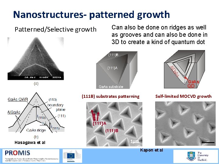
Nanostructures- patterned growth Can also be done on ridges as well as grooves and can also be done in 3 D to create a kind of quantum dot Patterned/Selective growth s a. A Al. G Ga. As QD (111 B) substrates patterning Self-limited MOCVD growth {111}A (111)B Hasagawa et al 1µm Kapon et al 21/09/2015 54

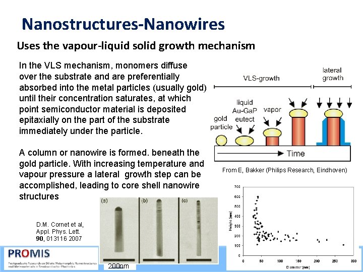
Nanostructures-Nanowires Uses the vapour-liquid solid growth mechanism In the VLS mechanism, monomers diffuse over the substrate and are preferentially absorbed into the metal particles (usually gold) until their concentration saturates, at which point semiconductor material is deposited epitaxially on the part of the substrate immediately under the particle. A column or nanowire is formed. beneath the gold particle. With increasing temperature and vapour pressure a lateral growth step can be accomplished, leading to core shell nanowire structures From E, Bakker (Philips Research, Eindhoven) D. M. Cornet et al, Appl. Phys. Lett. 90, 013116 2007 21/09/2015 200 nm 55

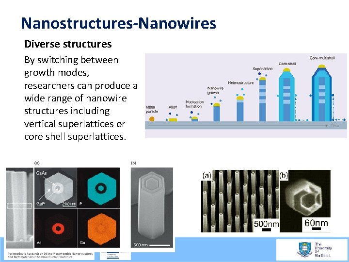
Nanostructures-Nanowires Diverse structures By switching between growth modes, researchers can produce a wide range of nanowire structures including vertical superlattices or core shell superlattices. 21/09/2015 56

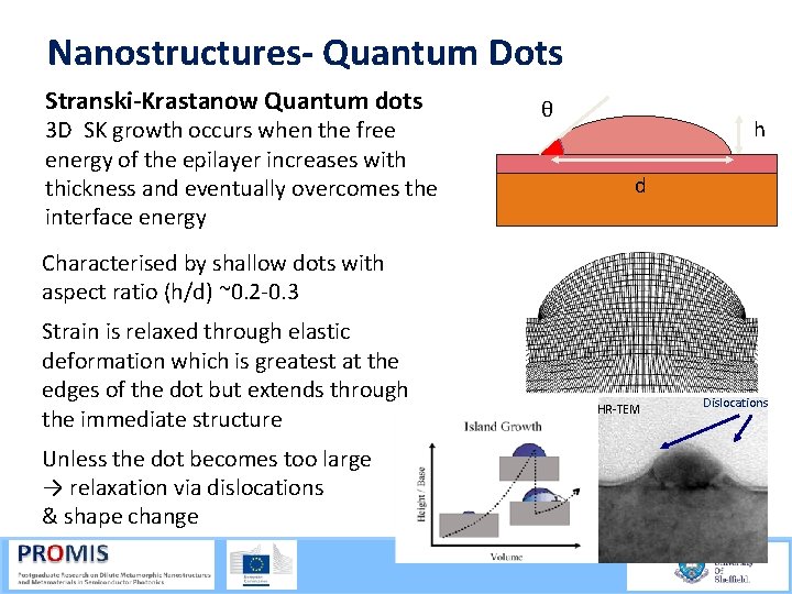
Nanostructures- Quantum Dots Stranski-Krastanow Quantum dots 3 D SK growth occurs when the free energy of the epilayer increases with thickness and eventually overcomes the interface energy θ h d Characterised by shallow dots with aspect ratio (h/d) ~0. 2 0. 3 Strain is relaxed through elastic deformation which is greatest at the edges of the dot but extends through the immediate structure HR TEM Dislocations Unless the dot becomes too large → relaxation via dislocations & shape change 21/09/2015 57

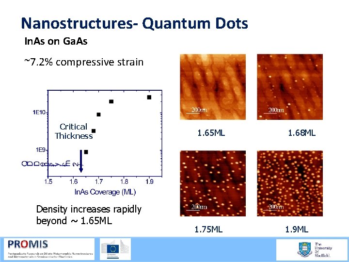
Nanostructures- Quantum Dots In. As on Ga. As ~7. 2% compressive strain Critical Thickness Density increases rapidly beyond ~ 1. 65 ML 21/09/2015 1. 65 ML 1. 75 ML 1. 68 ML 1. 9 ML 58

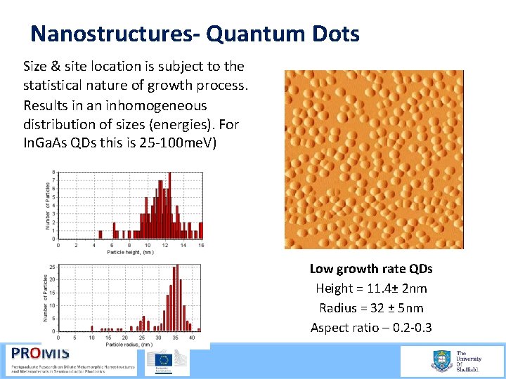
Nanostructures- Quantum Dots Size & site location is subject to the statistical nature of growth process. Results in an inhomogeneous distribution of sizes (energies). For In. Ga. As QDs this is 25 100 me. V) Low growth rate QDs Height = 11. 4± 2 nm Radius = 32 ± 5 nm Aspect ratio – 0. 2 0. 3 21/09/2015 59

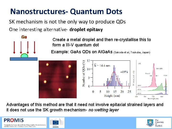
Nanostructures- Quantum Dots SK mechanism is not the only way to produce QDs One interesting alternative droplet epitaxy As Ga Create a metal droplet and then re-crystallise this to form a III-V quantum dot Example: Ga. As QDs on Al. Ga. As (Sakoda et al, Tsukuba, Japan) Advantages of this method are that it need not involve epitaxial strained layers and it does not use the SK growth mechanism- no wetting layer 21/09/2015 60

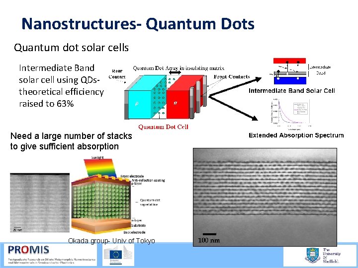
Nanostructures- Quantum Dots Quantum dot solar cells Intermediate Band solar cell using QDs theoretical efficiency raised to 63% Need a large number of stacks to give sufficient absorption Okada group- Univ of Tokyo 21/09/2015 61

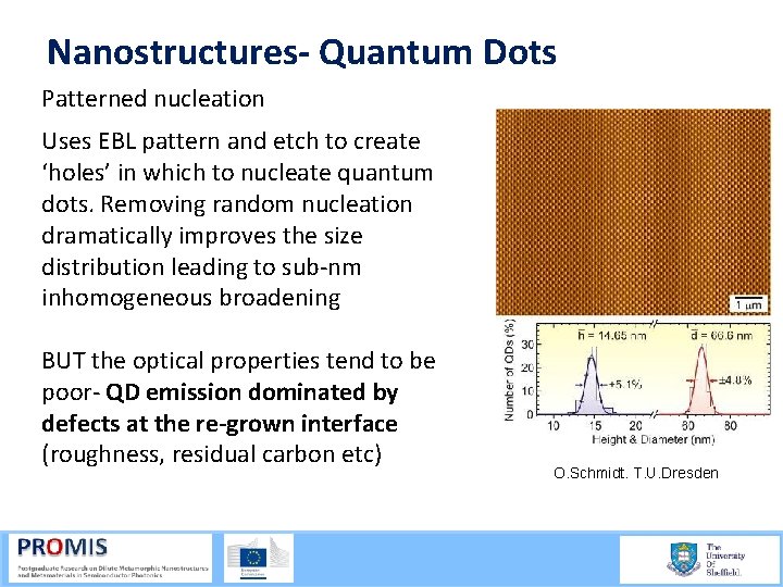
Nanostructures- Quantum Dots Patterned nucleation Uses EBL pattern and etch to create ‘holes’ in which to nucleate quantum dots. Removing random nucleation dramatically improves the size distribution leading to sub nm inhomogeneous broadening BUT the optical properties tend to be poor QD emission dominated by defects at the re-grown interface (roughness, residual carbon etc) 21/09/2015 O. Schmidt. T. U. Dresden 62