Surface Science and Thin Film Physics Adolf Winkler


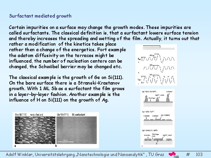
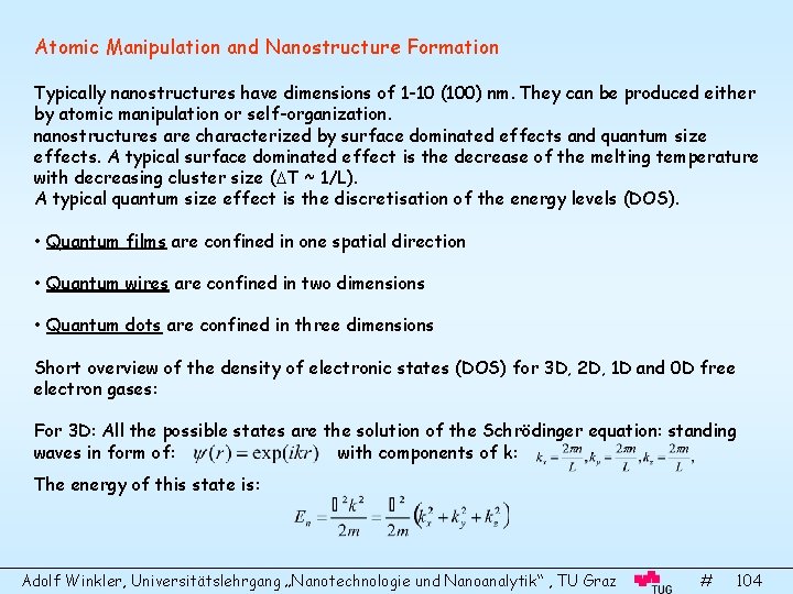
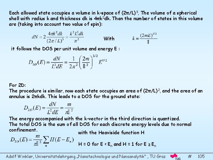
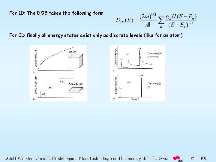
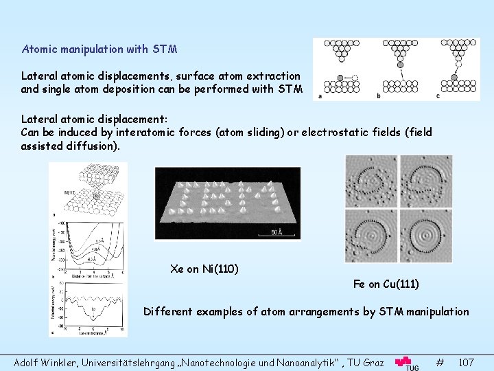
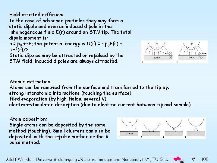
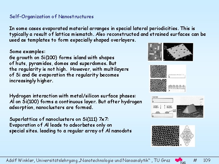
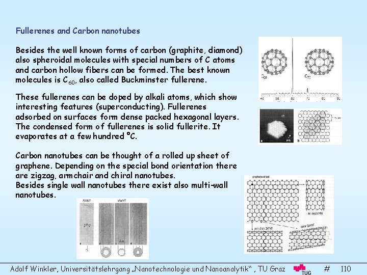
- Slides: 110

Surface Science and Thin Film Physics Adolf Winkler Institute of Solid State Physics, TU Graz Literature: K. Oura et al. , Surface Science, Springer Verlag, 2003 (ISBN 3 -540 -00545 -5; TU Bibliothek I 190. 293) Contents: 1. 2. 3. 4. 5. 6. 7. 8. 9. 10. 11. 12. 13. Experimental Background – UHV Technology Surface Analysis I: Diffraction Methods Surface Analysis II: Electron Spectroscopy Methods Surface Analysis III: Probing Surfaces with Ions Surface Analysis IV: Microscopy Atomic Structure on Clean Surfaces Atomic Structure of Surfaces with Adsorbates Structural Defects at Surfaces Electronic Structure of Surfaces Adsorption and Desorption Surface Diffusion Growth of Thin Films Atomic Manipulation and Nanostructure Formation Adolf Winkler, Universitätslehrgang „Nanotechnologie und Nanoanalytik“ , TU Graz # 1

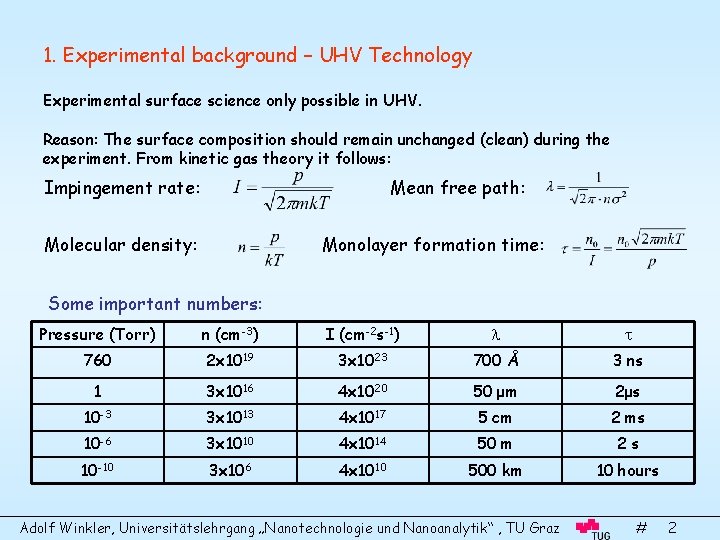
1. Experimental background – UHV Technology Experimental surface science only possible in UHV. Reason: The surface composition should remain unchanged (clean) during the experiment. From kinetic gas theory it follows: Impingement rate: Mean free path: Molecular density: Monolayer formation time: Some important numbers: Pressure (Torr) n (cm-3) I (cm-2 s-1) 760 2 x 10¹⁹ 3 x 10²³ 700 Å 3 ns 1 3 x 10¹⁶ 4 x 10²⁰ 50 μm 2μs 10 -3 3 x 10¹³ 4 x 10¹⁷ 5 cm 2 ms 10 -6 3 x 10¹⁰ 4 x 10¹⁴ 50 m 2 s 10 -10 3 x 10⁶ 4 x 10¹⁰ 500 km 10 hours Adolf Winkler, Universitätslehrgang „Nanotechnologie und Nanoanalytik“ , TU Graz # 2

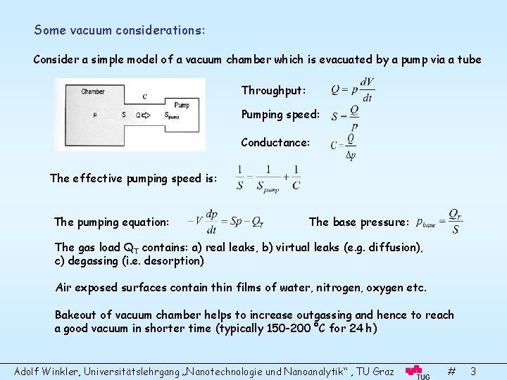
Some vacuum considerations: Consider a simple model of a vacuum chamber which is evacuated by a pump via a tube Throughput: Pumping speed: Conductance: The effective pumping speed is: The pumping equation: The base pressure: The gas load QT contains: a) real leaks, b) virtual leaks (e. g. diffusion), c) degassing (i. e. desorption) Air exposed surfaces contain thin films of water, nitrogen, oxygen etc. Bakeout of vacuum chamber helps to increase outgassing and hence to reach a good vacuum in shorter time (typically 150 -200 °C for 24 h) Adolf Winkler, Universitätslehrgang „Nanotechnologie und Nanoanalytik“ , TU Graz # 3

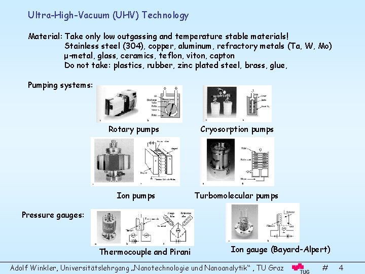
Ultra-High-Vacuum (UHV) Technology Material: Take only low outgassing and temperature stable materials! Stainless steel (304), copper, aluminum, refractory metals (Ta, W, Mo) μ-metal, glass, ceramics, teflon, viton, capton Do not take: plastics, rubber, zinc plated steel, brass, glue, Pumping systems: Rotary pumps Cryosorption pumps Ion pumps Turbomolecular pumps Pressure gauges: Thermocouple and Pirani Ion gauge (Bayard-Alpert) Adolf Winkler, Universitätslehrgang „Nanotechnologie und Nanoanalytik“ , TU Graz # 4

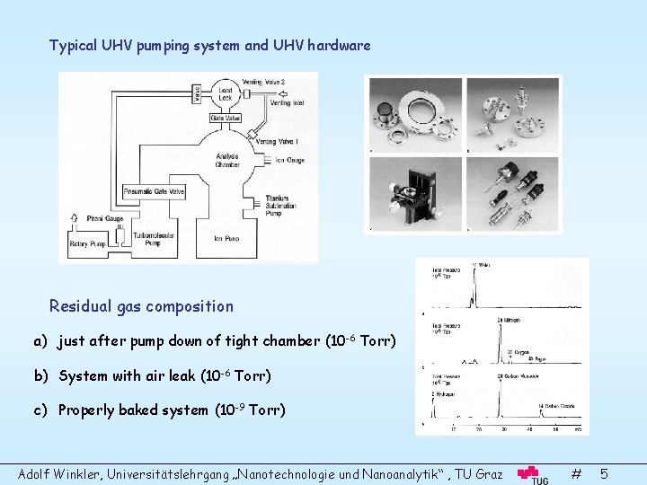
Typical UHV pumping system and UHV hardware Residual gas composition a) just after pump down of tight chamber (10 -6 Torr) b) System with air leak (10 -6 Torr) c) Properly baked system (10 -9 Torr) Adolf Winkler, Universitätslehrgang „Nanotechnologie und Nanoanalytik“ , TU Graz # 5

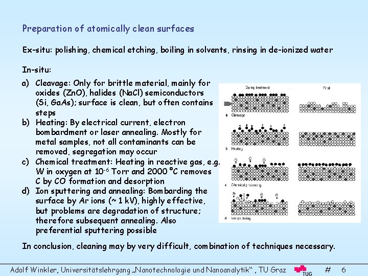
Preparation of atomically clean surfaces Ex-situ: polishing, chemical etching, boiling in solvents, rinsing in de-ionized water In-situ: a) Cleavage: Only for brittle material, mainly for oxides (Zn. O), halides (Na. Cl) semiconductors (Si, Ga. As); surface is clean, but often contains steps b) Heating: By electrical current, electron bombardment or laser annealing. Mostly for metal samples, not all contaminants can be removed, segregation may occur c) Chemical treatment: Heating in reactive gas, e. g. W in oxygen at 10 -6 Torr and 2000 °C removes C by CO formation and desorption d) Ion sputtering and annealing: Bombarding the surface by Ar ions (~ 1 k. V), highly effective, but problems are degradation of structure; therefore subsequent annealing. Also preferential sputtering possible In conclusion, cleaning may by very difficult, combination of techniques necessary. Adolf Winkler, Universitätslehrgang „Nanotechnologie und Nanoanalytik“ , TU Graz # 6

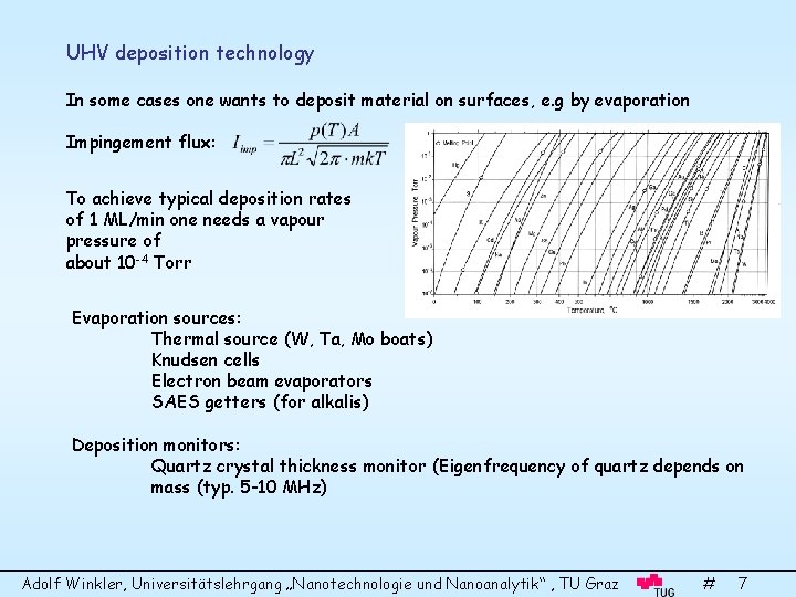
UHV deposition technology In some cases one wants to deposit material on surfaces, e. g by evaporation Impingement flux: To achieve typical deposition rates of 1 ML/min one needs a vapour pressure of about 10 -4 Torr Evaporation sources: Thermal source (W, Ta, Mo boats) Knudsen cells Electron beam evaporators SAES getters (for alkalis) Deposition monitors: Quartz crystal thickness monitor (Eigenfrequency of quartz depends on mass (typ. 5 -10 MHz) Adolf Winkler, Universitätslehrgang „Nanotechnologie und Nanoanalytik“ , TU Graz # 7

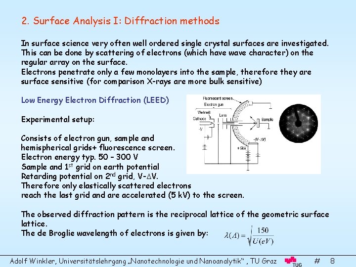
2. Surface Analysis I: Diffraction methods In surface science very often well ordered single crystal surfaces are investigated. This can be done by scattering of electrons (which have wave character) on the regular array on the surface. Electrons penetrate only a few monolayers into the sample, therefore they are surface sensitive (for comparison X-rays are more bulk sensitive) Low Energy Electron Diffraction (LEED) Experimental setup: Consists of electron gun, sample and hemispherical grids+ fluorescence screen. Electron energy typ. 50 – 300 V Sample and 1 st grid on earth potential Retarding potential on 2 nd grid, V-ΔV. Therefore only elastically scattered electrons reach the last grid and are accelerated (5 k. V) to the screen. The observed diffraction pattern is the reciprocal lattice of the geometric surface lattice. The de Broglie wavelength of electrons is given by: Adolf Winkler, Universitätslehrgang „Nanotechnologie und Nanoanalytik“ , TU Graz # 8

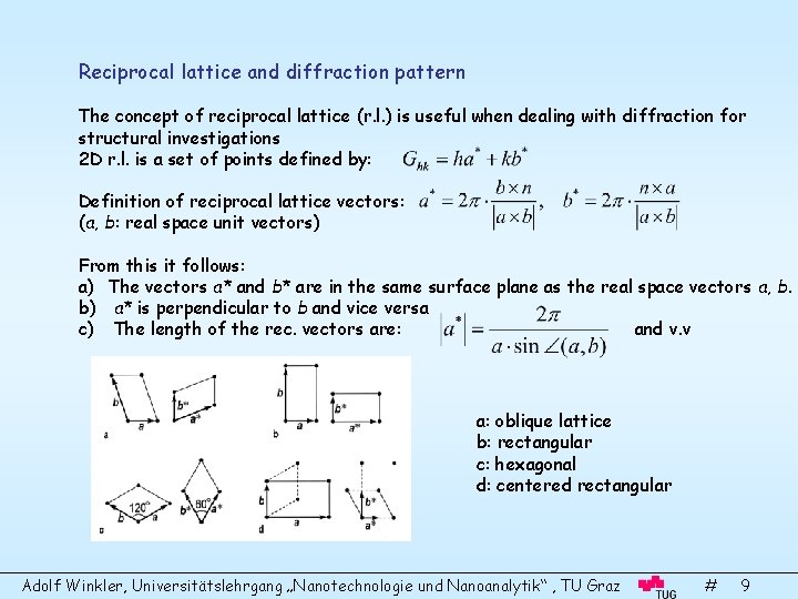
Reciprocal lattice and diffraction pattern The concept of reciprocal lattice (r. l. ) is useful when dealing with diffraction for structural investigations 2 D r. l. is a set of points defined by: Definition of reciprocal lattice vectors: (a, b: real space unit vectors) From this it follows: a) The vectors a* and b* are in the same surface plane as the real space vectors a, b. b) a* is perpendicular to b and vice versa c) The length of the rec. vectors are: and v. v a: oblique lattice b: rectangular c: hexagonal d: centered rectangular Adolf Winkler, Universitätslehrgang „Nanotechnologie und Nanoanalytik“ , TU Graz # 9

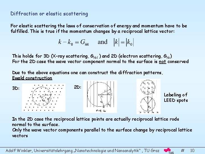
Diffraction or elastic scattering For elastic scattering the laws of conservation of energy and momentum have to be fulfilled. This is true if the momentum changes by a reciprocal lattice vector: This holds for 3 D (X-ray scattering, Ghkl ) and 2 D (electron scattering, Ghk) For the 2 D case the wave vector component normal to the surface is not conserved Due to the above equations one can construct the diffraction patterns, Ewald construction 3 D: 2 D: Labeling of LEED spots In the 2 D case the reciprocal lattice points are actually reciprocal lattice rods normal to the surface. Only the wave vector components parallel to the surface change by reciprocal lattice vectors Adolf Winkler, Universitätslehrgang „Nanotechnologie und Nanoanalytik“ , TU Graz # 10

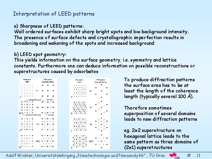
Interpretation of LEED patterns a) Sharpness of LEED patterns: Well ordered surfaces exhibit sharp bright spots and low background intensity. The presence of surface defects and crystallographic imperfection results in broadening and wakening of the spots and increased background b) LEED spot geometry: This yields information on the surface geometry, i. e. symmetry and lattice constants. Furthermore one can deduce information on possible reconstructions or superstructures caused by adsorbates To produce diffraction patterns the surface area has to be at least the length of the coherence length (typically several 100 Å). Therefore sometimes superposition of several domains leads to new diffraction patterns eg. 2 x 2 superstructure on hexagonal lattice leads to the same pattern as three domains of (2 x 1) superstructures Adolf Winkler, Universitätslehrgang „Nanotechnologie und Nanoanalytik“ , TU Graz # 11

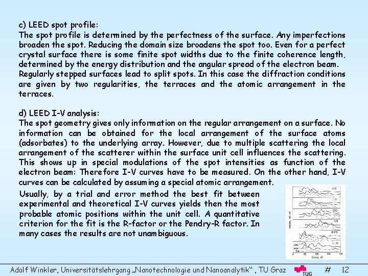
c) LEED spot profile: The spot profile is determined by the perfectness of the surface. Any imperfections broaden the spot. Reducing the domain size broadens the spot too. Even for a perfect crystal surface there is some finite spot widths due to the finite coherence length, determined by the energy distribution and the angular spread of the electron beam. Regularly stepped surfaces lead to split spots. In this case the diffraction conditions are given by two regularities, the terraces and the atomic arrangement in the terraces. d) LEED I-V analysis: The spot geometry gives only information on the regular arrangement on a surface. No information can be obtained for the local arrangement of the surface atoms (adsorbates) to the underlying array. However, due to multiple scattering the local arrangement of the scatterer within the surface unit cell influences the scattering. This shows up in special modulations of the spot intensities as function of the electron beam: Therefore I-V curves have to be measured. On the other hand, I-V curves can be calculated by assuming a special atomic arrangement. Usually, by a trial and error method the best fit between experimental and theoretical I-V curves yields then the most probable atomic positions within the unit cell. A quantitative criterion for the fit is the R-factor or the Pendry-R factor. In many cases the results are not unambiguous. Adolf Winkler, Universitätslehrgang „Nanotechnologie und Nanoanalytik“ , TU Graz # 12

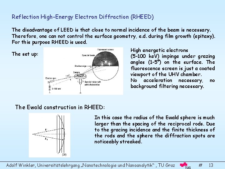
Reflection High-Energy Electron Diffraction (RHEED) The disadvantage of LEED is that close to normal incidence of the beam is necessary. Therefore, one can not control the surface geometry, e. d. during film growth (epitaxy). For this purpose RHEED is used. High energetic electrons (5 -100 ke. V) impinge under grazing angles (1 -5°) on the surface. The fluorescence screen is just a coated viewport of the UHV chamber. No acceleration necessary, no background filtering necessary. The set up: The Ewald construction in RHEED: In this case the radius of the Ewald sphere is much larger than the spacing of the reciprocal rods. Due to the gracing incidence and the finite thickness of the rods and the sphere the diffraction spots are noticeably streaked. Adolf Winkler, Universitätslehrgang „Nanotechnologie und Nanoanalytik“ , TU Graz # 13

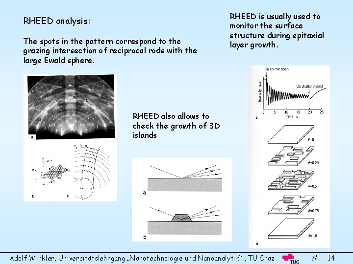
RHEED analysis: The spots in the pattern correspond to the grazing intersection of reciprocal rods with the large Ewald sphere. RHEED is usually used to monitor the surface structure during epitaxial layer growth. RHEED also allows to check the growth of 3 D islands Adolf Winkler, Universitätslehrgang „Nanotechnologie und Nanoanalytik“ , TU Graz # 14

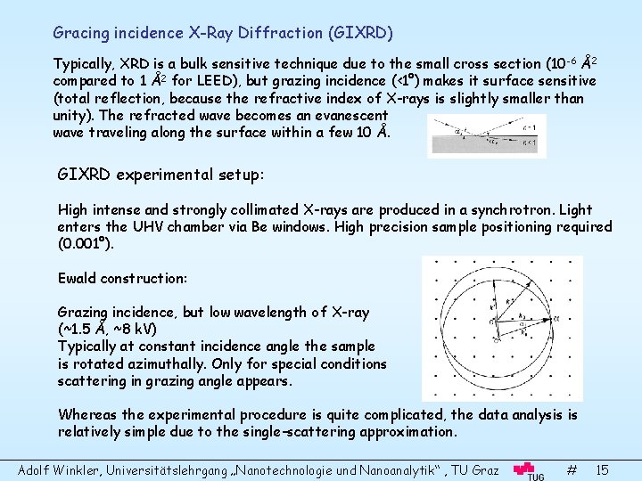
Gracing incidence X-Ray Diffraction (GIXRD) Typically, XRD is a bulk sensitive technique due to the small cross section (10 -6 Å2 compared to 1 Å2 for LEED), but grazing incidence (<1°) makes it surface sensitive (total reflection, because the refractive index of X-rays is slightly smaller than unity). The refracted wave becomes an evanescent wave traveling along the surface within a few 10 Å. GIXRD experimental setup: High intense and strongly collimated X-rays are produced in a synchrotron. Light enters the UHV chamber via Be windows. High precision sample positioning required (0. 001°). Ewald construction: Grazing incidence, but low wavelength of X-ray (~1. 5 Å, ~8 k. V) Typically at constant incidence angle the sample is rotated azimuthally. Only for special conditions scattering in grazing angle appears. Whereas the experimental procedure is quite complicated, the data analysis is relatively simple due to the single-scattering approximation. Adolf Winkler, Universitätslehrgang „Nanotechnologie und Nanoanalytik“ , TU Graz # 15

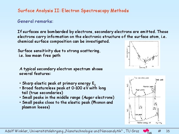
Surface Analysis II: Electron Spectroscopy Methods General remarks: If surfaces are bombarded by electrons, secondary electrons are emitted. These electrons carry information on the electronic structure of the surface atom, i. e. chemical surface composition can be investigated. Surface sensitivity due to strong scattering, i. e. low mean free path A typical secondary electron spectrum shows several features: • Sharp elastic peak at primary energy Ep • Broad featureless peak at 0 -100 e. V with long tail (true secondaries) • Small peaks in the middle range (Auger electrons) • Small peaks close to the elastic peak (Phonon and plasmon losses) Adolf Winkler, Universitätslehrgang „Nanotechnologie und Nanoanalytik“ , TU Graz # 16

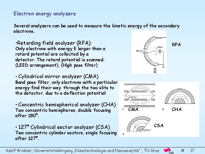
Electron energy analyzers Several analyzers can be used to measure the kinetic energy of the secondary electrons. • Retarding field analyzer (RFA): RFA Only electrons with energy E larger than a retard potential are collected by a detector. The retard potential is scanned. (LEED arrangement). (High pass filter) • Cylindrical mirror analyzer (CMA) Band pass filter, only electrons with a particular energy find their way through the two slits to the detector, due to a deflection potential • Concentric hemispherical analyzer (CHA) Two concentric hemispheres, double focusing after 180°. • 127° Cylindrical sector analyzer (CSA) Two concentric cylinder sectors, single focusing after 127°. CMA CHA CSA Adolf Winkler, Universitätslehrgang „Nanotechnologie und Nanoanalytik“ , TU Graz # 17

Auger Electron Spectroscopy Is the most commonly used method to investigate surface composition. The principle is as follows: An impinging electron (2 -10 ke. V) creates a core hole and both electrons leave the surface. The ionized atom relaxes by emitting either an Xray photon (X-ray fluorescence) or by ejecting another electron (Auger electron). For lighter elements Auger emission is favored over X-ray fluorescence. Three electrons are involved in the Auger process, therefore H and He do not produce Auger electrons. The energy of the Auger electrons depends on the energy levels of the atom: However, this is a rough estimate, because the final state is an ion and the levels may shift compared to the neutral atom. Φ: Work function (energy needed to bring an electron from the Fermi level to the vacuum level) Adolf Winkler, Universitätslehrgang „Nanotechnologie und Nanoanalytik“ , TU Graz # 18

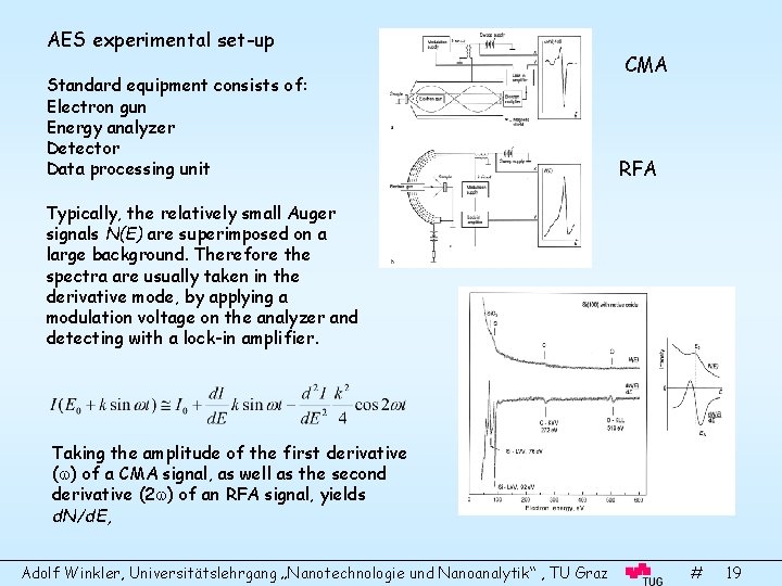
AES experimental set-up Standard equipment consists of: Electron gun Energy analyzer Detector Data processing unit CMA RFA Typically, the relatively small Auger signals N(E) are superimposed on a large background. Therefore the spectra are usually taken in the derivative mode, by applying a modulation voltage on the analyzer and detecting with a lock-in amplifier. Taking the amplitude of the first derivative ( ) of a CMA signal, as well as the second derivative (2 ) of an RFA signal, yields d. N/d. E, Adolf Winkler, Universitätslehrgang „Nanotechnologie und Nanoanalytik“ , TU Graz # 19

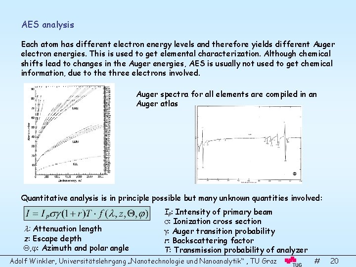
AES analysis Each atom has different electron energy levels and therefore yields different Auger electron energies. This is used to get elemental characterization. Although chemical shifts lead to changes in the Auger energies, AES is usually not used to get chemical information, due to the three electrons involved. Auger spectra for all elements are compiled in an Auger atlas Quantitative analysis is in principle possible but many unknown quantities involved: : Attenuation length z: Escape depth , : Azimuth and polar angle IP: Intensity of primary beam : Ionization cross section : Auger transition probability r: Backscattering factor T: Transmission probability of analyzer Adolf Winkler, Universitätslehrgang „Nanotechnologie und Nanoanalytik“ , TU Graz # 20

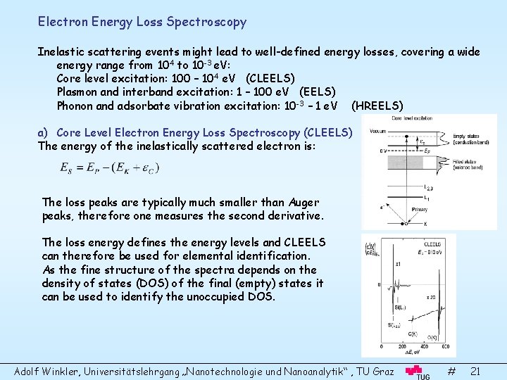
Electron Energy Loss Spectroscopy Inelastic scattering events might lead to well-defined energy losses, covering a wide energy range from 104 to 10 -3 e. V: Core level excitation: 100 – 104 e. V (CLEELS) Plasmon and interband excitation: 1 – 100 e. V (EELS) Phonon and adsorbate vibration excitation: 10 -3 – 1 e. V (HREELS) a) Core Level Electron Energy Loss Spectroscopy (CLEELS) The energy of the inelastically scattered electron is: The loss peaks are typically much smaller than Auger peaks, therefore one measures the second derivative. The loss energy defines the energy levels and CLEELS can therefore be used for elemental identification. As the fine structure of the spectra depends on the density of states (DOS) of the final (empty) states it can be used to identify the unoccupied DOS. Adolf Winkler, Universitätslehrgang „Nanotechnologie und Nanoanalytik“ , TU Graz # 21

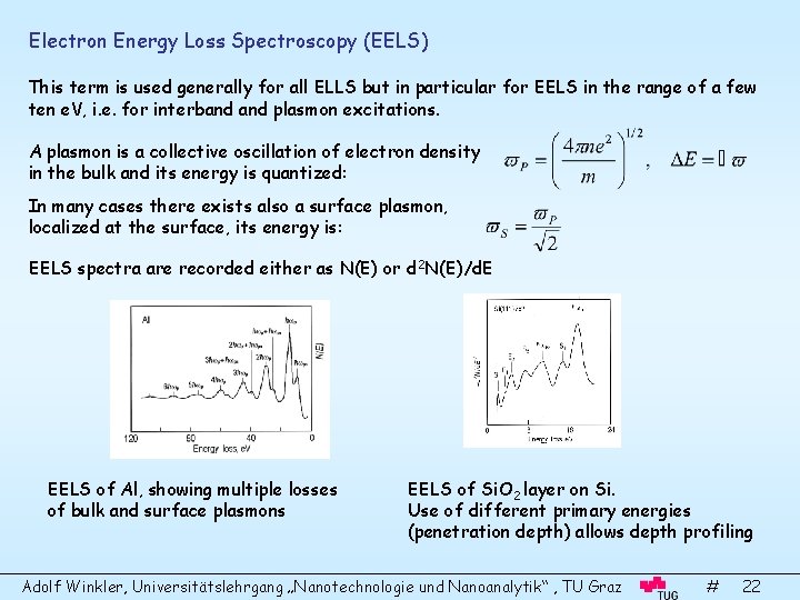
Electron Energy Loss Spectroscopy (EELS) This term is used generally for all ELLS but in particular for EELS in the range of a few ten e. V, i. e. for interband plasmon excitations. A plasmon is a collective oscillation of electron density in the bulk and its energy is quantized: In many cases there exists also a surface plasmon, localized at the surface, its energy is: EELS spectra are recorded either as N(E) or d 2 N(E)/d. E EELS of Al, showing multiple losses of bulk and surface plasmons EELS of Si. O 2 layer on Si. Use of different primary energies (penetration depth) allows depth profiling Adolf Winkler, Universitätslehrgang „Nanotechnologie und Nanoanalytik“ , TU Graz # 22

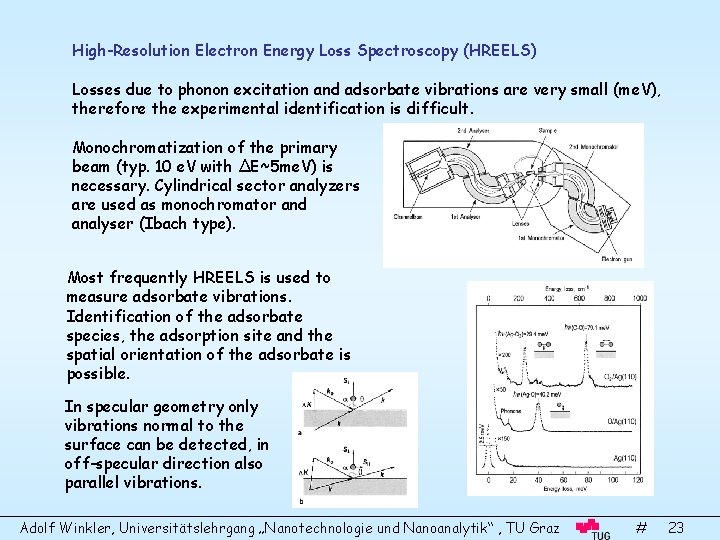
High-Resolution Electron Energy Loss Spectroscopy (HREELS) Losses due to phonon excitation and adsorbate vibrations are very small (me. V), therefore the experimental identification is difficult. Monochromatization of the primary beam (typ. 10 e. V with ΔE~5 me. V) is necessary. Cylindrical sector analyzers are used as monochromator and analyser (Ibach type). Most frequently HREELS is used to measure adsorbate vibrations. Identification of the adsorbate species, the adsorption site and the spatial orientation of the adsorbate is possible. In specular geometry only vibrations normal to the surface can be detected, in off-specular direction also parallel vibrations. Adolf Winkler, Universitätslehrgang „Nanotechnologie und Nanoanalytik“ , TU Graz # 23

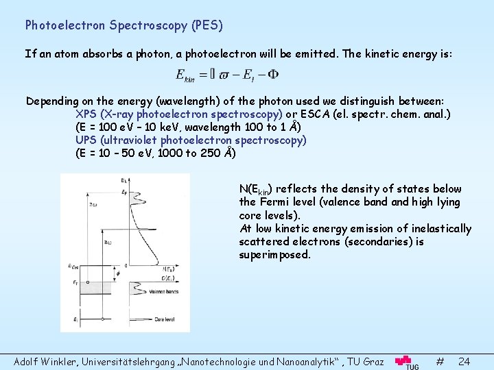
Photoelectron Spectroscopy (PES) If an atom absorbs a photon, a photoelectron will be emitted. The kinetic energy is: Depending on the energy (wavelength) of the photon used we distinguish between: XPS (X-ray photoelectron spectroscopy) or ESCA (el. spectr. chem. anal. ) (E = 100 e. V – 10 ke. V, wavelength 100 to 1 Å) UPS (ultraviolet photoelectron spectroscopy) (E = 10 – 50 e. V, 1000 to 250 Å) N(Ekin) reflects the density of states below the Fermi level (valence band high lying core levels). At low kinetic energy emission of inelastically scattered electrons (secondaries) is superimposed. Adolf Winkler, Universitätslehrgang „Nanotechnologie und Nanoanalytik“ , TU Graz # 24

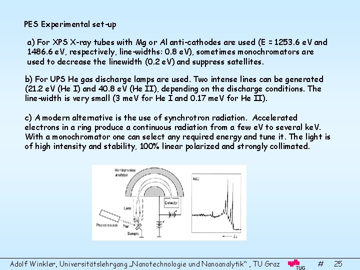
PES Experimental set-up a) For XPS X-ray tubes with Mg or Al anti-cathodes are used (E = 1253. 6 e. V and 1486. 6 e. V, respectively, line-widths: 0. 8 e. V), sometimes monochromators are used to decrease the linewidth (0. 2 e. V) and suppress satellites. b) For UPS He gas discharge lamps are used. Two intense lines can be generated (21. 2 e. V (He I) and 40. 8 e. V (He II), depending on the discharge conditions. The line-width is very small (3 me. V for He I and 0. 17 me. V for He II). c) A modern alternative is the use of synchrotron radiation. Accelerated electrons in a ring produce a continuous radiation from a few e. V to several ke. V. With a monochromator one can select any required energy and tune it. The light is of high intensity and stability, 100% linear polarized and strongly collimated. Adolf Winkler, Universitätslehrgang „Nanotechnologie und Nanoanalytik“ , TU Graz # 25

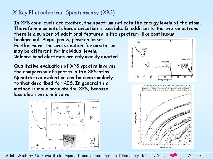
X-Ray Photoelectron Spectroscopy (XPS) In XPS core levels are excited, the spectrum reflects the energy levels of the atom. Therefore elemental characterization is possible. In addition to the photoelectrons there is a number of additional features in the spectrum, like continuous background, Auger peaks, plasmon losses. Furthermore, the cross section for excitation may be different for individual levels. Valence band electrons are only weakly excited. Qualitative evaluation of XPS spectra involves the comparison of spectra in the XPS-atlas. Quantitative evaluation can be done similarly to that described for AES. In general this method is more accurate for XPS, because less electrons are involve. Ni Adolf Winkler, Universitätslehrgang „Nanotechnologie und Nanoanalytik“ , TU Graz # 26

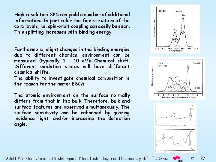
High resolution XPS can yield a number of additional information: In particular the fine structure of the core levels, i. e. spin-orbit coupling can easily be seen. This splitting increases with binding energy. Furthermore, slight changes in the binding energies due to different chemical environment can be measured (typically 1 – 10 e. V): Chemical shift. Different oxidation states will have different chemical shifts. The ability to investigate chemical composition is the reason for the name: ESCA The atomic environment on the surface normally differs from that in the bulk. Therefore, bulk and surface features are observed simultaneously. The surface sensitivity can be enhanced by grazing incidence light, and/or increasing the detection angle. Adolf Winkler, Universitätslehrgang „Nanotechnologie und Nanoanalytik“ , TU Graz # 27

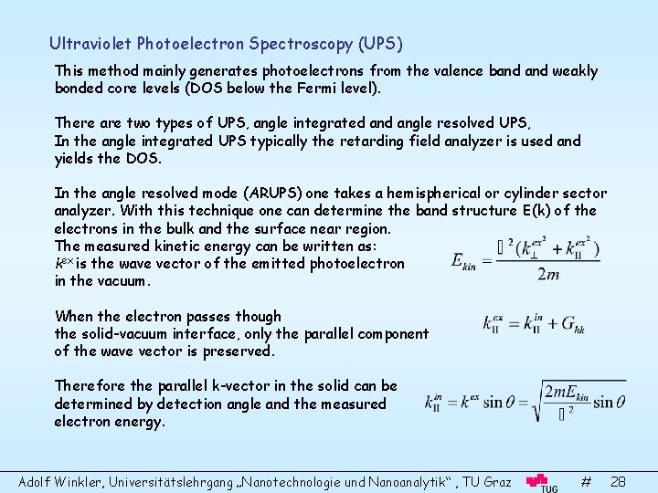
Ultraviolet Photoelectron Spectroscopy (UPS) This method mainly generates photoelectrons from the valence band weakly bonded core levels (DOS below the Fermi level). There are two types of UPS, angle integrated angle resolved UPS, In the angle integrated UPS typically the retarding field analyzer is used and yields the DOS. In the angle resolved mode (ARUPS) one takes a hemispherical or cylinder sector analyzer. With this technique one can determine the band structure E(k) of the electrons in the bulk and the surface near region. The measured kinetic energy can be written as: kex is the wave vector of the emitted photoelectron in the vacuum. When the electron passes though the solid-vacuum interface, only the parallel component of the wave vector is preserved. Therefore the parallel k-vector in the solid can be determined by detection angle and the measured electron energy. Adolf Winkler, Universitätslehrgang „Nanotechnologie und Nanoanalytik“ , TU Graz # 28

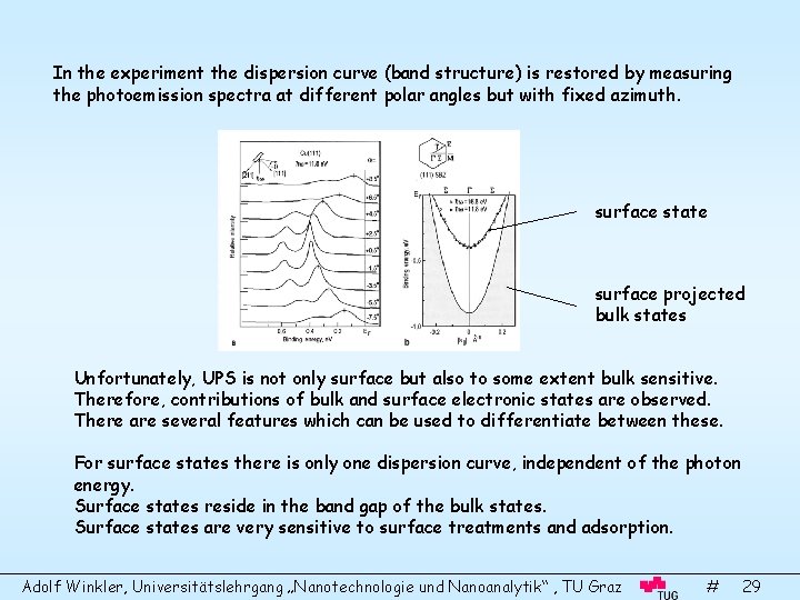
In the experiment the dispersion curve (band structure) is restored by measuring the photoemission spectra at different polar angles but with fixed azimuth. surface state surface projected bulk states Unfortunately, UPS is not only surface but also to some extent bulk sensitive. Therefore, contributions of bulk and surface electronic states are observed. There are several features which can be used to differentiate between these. For surface states there is only one dispersion curve, independent of the photon energy. Surface states reside in the band gap of the bulk states. Surface states are very sensitive to surface treatments and adsorption. Adolf Winkler, Universitätslehrgang „Nanotechnologie und Nanoanalytik“ , TU Graz # 29

Surface Analysis III: Probing Surfaces with Ions The most widely used techniques are the following: • Ions Scattering Spectroscopy (ISS) (ions elastically scattered from the surface are energy analyzed) • Low-energy ion scattering spectroscopy (LEIS), (1 -20 ke. V) • Medium-energy ion scattering spectroscopy (MEIS), (20 – 200 ke. V) • High energy ion scattering (HEIS) or Rutherford backscattering (RBS) ( 200 ke. V – 2 Me. V) • Elastic Recoil Detection Analysis (ERDA) (target atoms or ions elastically recoiled by primary ions are energy analyzed) • Secondary Ion Mass Spectroscopy (SIMS) (ions sputtered from a surface by a primary beam are mass analyzed) The major application concerns elemental composition and atomic structure of surfaces. Structural analysis is based on real space considerations. Mainly short range arrangements of neighboring surface atoms can be investigated Adolf Winkler, Universitätslehrgang „Nanotechnologie und Nanoanalytik“ , TU Graz # 30

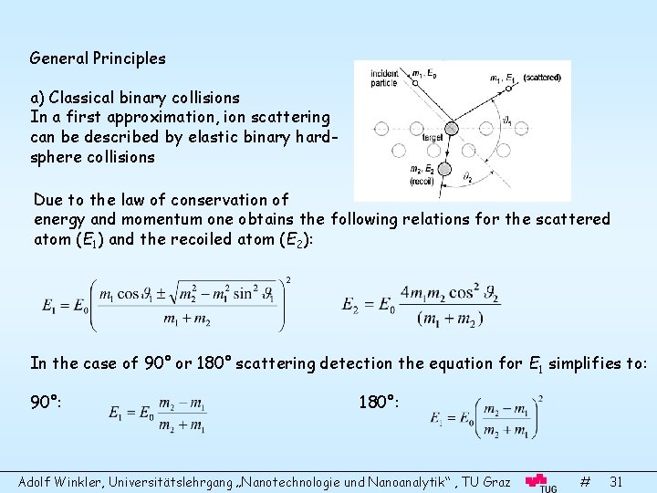
General Principles a) Classical binary collisions In a first approximation, ion scattering can be described by elastic binary hardsphere collisions Due to the law of conservation of energy and momentum one obtains the following relations for the scattered atom (E 1) and the recoiled atom (E 2): In the case of 90° or 180° scattering detection the equation for E 1 simplifies to: 90°: 180°: Adolf Winkler, Universitätslehrgang „Nanotechnologie und Nanoanalytik“ , TU Graz # 31

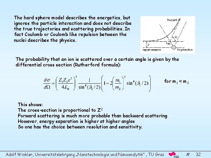
The hard sphere model describes the energetics, but ignores the particle interaction and does not describe the true trajectories and scattering probabilities. In fact Coulomb or Coulomb like repulsion between the nuclei describes the physics. The probability that an ion is scattered over a certain angle is given by the differential cross section (Rutherford formula): for m 1 « m 2 This shows: The cross-section is proportional to Z 2 Forward scattering is much more probable than backward scattering However, energy separation is higher at higher angles So one has the choice between resolution and sensitivity. Adolf Winkler, Universitätslehrgang „Nanotechnologie und Nanoanalytik“ , TU Graz # 32

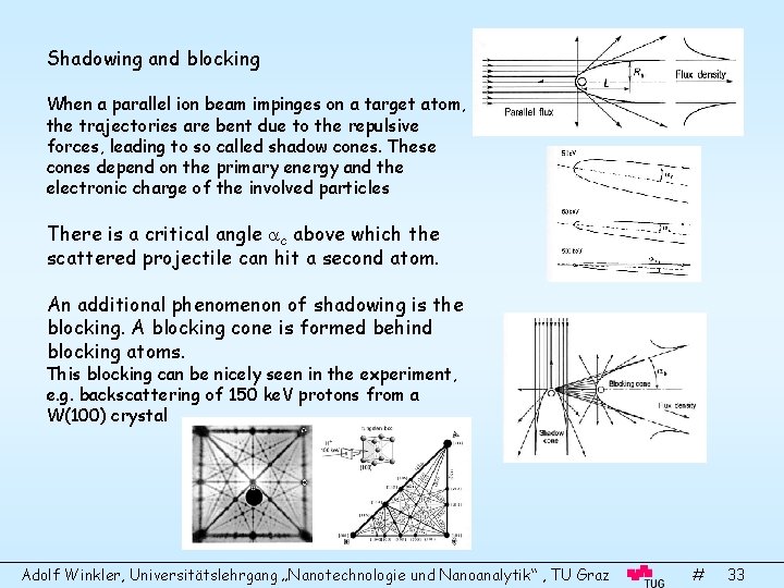
Shadowing and blocking When a parallel ion beam impinges on a target atom, the trajectories are bent due to the repulsive forces, leading to so called shadow cones. These cones depend on the primary energy and the electronic charge of the involved particles There is a critical angle c above which the scattered projectile can hit a second atom. An additional phenomenon of shadowing is the blocking. A blocking cone is formed behind blocking atoms. This blocking can be nicely seen in the experiment, e. g. backscattering of 150 ke. V protons from a W(100) crystal Adolf Winkler, Universitätslehrgang „Nanotechnologie und Nanoanalytik“ , TU Graz # 33

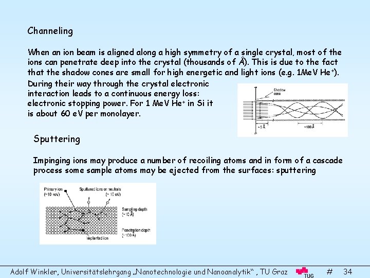
Channeling When an ion beam is aligned along a high symmetry of a single crystal, most of the ions can penetrate deep into the crystal (thousands of Å). This is due to the fact that the shadow cones are small for high energetic and light ions (e. g. 1 Me. V He +). During their way through the crystal electronic interaction leads to a continuous energy loss: electronic stopping power. For 1 Me. V He+ in Si it is about 60 e. V per monolayer. Sputtering Impinging ions may produce a number of recoiling atoms and in form of a cascade process some sample atoms may be ejected from the surfaces: sputtering Adolf Winkler, Universitätslehrgang „Nanotechnologie und Nanoanalytik“ , TU Graz # 34

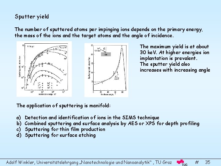
Sputter yield The number of sputtered atoms per impinging ions depends on the primary energy, the mass of the ions and the target atoms and the angle of incidence. The maximum yield is at about 30 ke. V. At higher energies ion implantation is prevalent. The sputter yield also increases with increasing angle The application of sputtering is manifold: a) b) c) d) Detection and identification of ions in the SIMS technique Combined sputtering and surface analysis by AES or XPS for depth profiling Sputtering for thin film production Sputtering for surface etching Adolf Winkler, Universitätslehrgang „Nanotechnologie und Nanoanalytik“ , TU Graz # 35

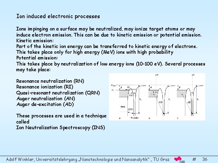
Ion induced electronic processes Ions impinging on a surface may be neutralized, may ionize target atoms or may induce electron emission. This can be due to kinetic emission or potential emission. Kinetic emission: Part of the kinetic ion energy can be transferred to kinetic energy of electrons. This takes place only for high energy (Me. V) ions with high probability Potential emission: This takes place by neutralization of low energy ions (10 -100 e. V). Several processes may take place: Resonance neutralization (RN) Resonance ionization (RI) Quasi-resonant neutralization (QRN) Auger neutralization (AN) Auger de-excitation (AD) These processes are used in a technique called Ion Neutralization Spectroscopy (INS) Adolf Winkler, Universitätslehrgang „Nanotechnologie und Nanoanalytik“ , TU Graz # 36

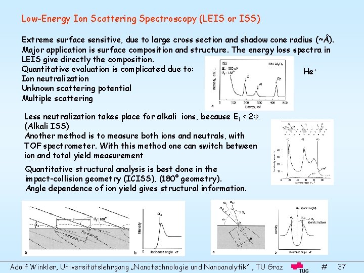
Low-Energy Ion Scattering Spectroscopy (LEIS or ISS) Extreme surface sensitive, due to large cross section and shadow cone radius (~Å). Major application is surface composition and structure. The energy loss spectra in LEIS give directly the composition. Quantitative evaluation is complicated due to: He+ Ion neutralization Unknown scattering potential Multiple scattering Less neutralization takes place for alkali ions, because Ei < 2Φ. (Alkali ISS) Another method is to measure both ions and neutrals, with TOF spectrometer. With this method one can switch between ion and total yield measurement Quantitative structural analysis is best done in the impact-collision geometry (ICISS), (180° geometry). Angle dependence of ion yield gives structural information. Adolf Winkler, Universitätslehrgang „Nanotechnologie und Nanoanalytik“ , TU Graz # 37

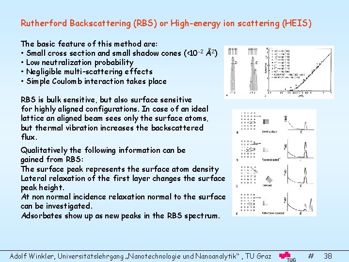
Rutherford Backscattering (RBS) or High-energy ion scattering (HEIS) The basic feature of this method are: • Small cross section and small shadow cones (<10 -2 Å2) • Low neutralization probability • Negligible multi-scattering effects • Simple Coulomb interaction takes place RBS is bulk sensitive, but also surface sensitive for highly aligned configurations. In case of an ideal lattice an aligned beam sees only the surface atoms, but thermal vibration increases the backscattered flux. Qualitatively the following information can be gained from RBS: The surface peak represents the surface atom density Lateral relaxation of the first layer changes the surface peak height. At non normal incidence relaxation normal to the surface can be investigated. Adsorbates show up as new peaks in the RBS spectrum. Adolf Winkler, Universitätslehrgang „Nanotechnologie und Nanoanalytik“ , TU Graz # 38

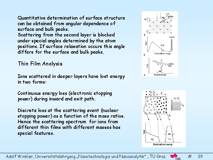
Quantitative determination of surface structure can be obtained from angular dependence of surface and bulk peaks. Scattering from the second layer is blocked under special angles determined by the atom positions. If surface relaxation occurs this angle differs for the surface and bulk peaks, Thin Film Analysis Ions scattered in deeper layers have lost energy in two forms: Continuous energy loss (electronic stopping power) during inward and exit path. Discrete loss at the scattering event (nuclear stopping power) as a function of the mass ratios. Hence the scattering spectrum for ions from different thin films with different masses has special features. Adolf Winkler, Universitätslehrgang „Nanotechnologie und Nanoanalytik“ , TU Graz # 39

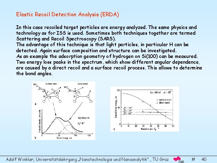
Elastic Recoil Detection Analysis (ERDA) In this case recoiled target particles are energy analyzed. The same physics and technology as for ISS is used. Sometimes both techniques together are termed Scattering and Recoil Spectroscopy (SARS). The advantage of this technique is that light particles, in particular H can be detected. Again surface composition and structure can be investigated. As an example the adsorption geometry of hydrogen on Si(100) can be measured. Two energy loss peaks in the spectrum, which show different angular dependence, are caused by a direct recoil and a surface recoil process. This allows to determine the bond angles. Adolf Winkler, Universitätslehrgang „Nanotechnologie und Nanoanalytik“ , TU Graz # 40

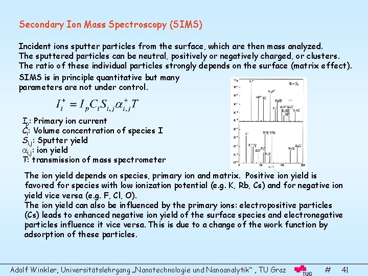
Secondary Ion Mass Spectroscopy (SIMS) Incident ions sputter particles from the surface, which are then mass analyzed. The sputtered particles can be neutral, positively or negatively charged, or clusters. The ratio of these individual particles strongly depends on the surface (matrix effect). SIMS is in principle quantitative but many parameters are not under control. Ip: Primary ion current Ci: Volume concentration of species I Si, j: Sputter yield i, j: ion yield T: transmission of mass spectrometer The ion yield depends on species, primary ion and matrix. Positive ion yield is favored for species with low ionization potential (e. g. K, Rb, Cs) and for negative ion yield vice versa (e. g. F, Cl, O). The ion yield can also be influenced by the primary ions: electropositive particles (Cs) leads to enhanced negative ion yield of the surface species and electronegative particles influence it vice versa. This is due to a change of the work function by adsorption of these particles. Adolf Winkler, Universitätslehrgang „Nanotechnologie und Nanoanalytik“ , TU Graz # 41

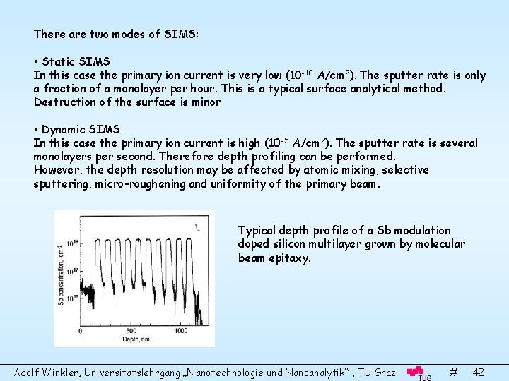
There are two modes of SIMS: • Static SIMS In this case the primary ion current is very low (10 -10 A/cm 2). The sputter rate is only a fraction of a monolayer per hour. This is a typical surface analytical method. Destruction of the surface is minor • Dynamic SIMS In this case the primary ion current is high (10 -5 A/cm 2). The sputter rate is several monolayers per second. Therefore depth profiling can be performed. However, the depth resolution may be affected by atomic mixing, selective sputtering, micro-roughening and uniformity of the primary beam. Typical depth profile of a Sb modulation doped silicon multilayer grown by molecular beam epitaxy. Adolf Winkler, Universitätslehrgang „Nanotechnologie und Nanoanalytik“ , TU Graz # 42

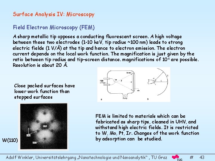
Surface Analysis IV: Microscopy Field Electron Microscopy (FEM) A sharp metallic tip opposes a conducting fluorescent screen. A high voltage between these two electrodes (1 -10 ke. V, tip radius ~100 nm) leads to strong electric fields (1 V/Å) at the tip and hence to electron emission. The electron current depends on the local work function. The magnification is just given by the ratio between tip radius and tip-screen distance. magnifications of 10 6 are possible. Resolution is about 20 Å. Close packed surfaces have lower work function than stepped surfaces W(110) FEM is limited to materials which can be fabricated as sharp tips, cleaned in UHV, and withstand high electric fields. It is restricted to W, Mo, Pt, Ir. Changes of the work function by adsorption can be studied. Adolf Winkler, Universitätslehrgang „Nanotechnologie und Nanoanalytik“ , TU Graz # 43

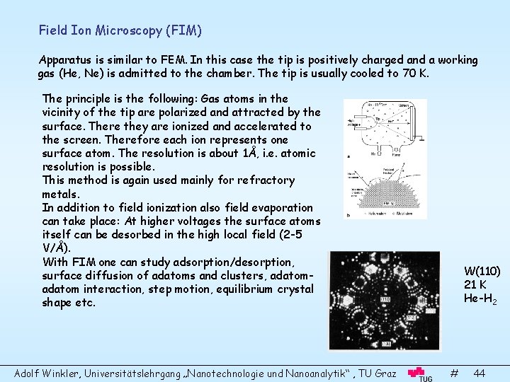
Field Ion Microscopy (FIM) Apparatus is similar to FEM. In this case the tip is positively charged and a working gas (He, Ne) is admitted to the chamber. The tip is usually cooled to 70 K. The principle is the following: Gas atoms in the vicinity of the tip are polarized and attracted by the surface. There they are ionized and accelerated to the screen. Therefore each ion represents one surface atom. The resolution is about 1Å, i. e. atomic resolution is possible. This method is again used mainly for refractory metals. In addition to field ionization also field evaporation can take place: At higher voltages the surface atoms itself can be desorbed in the high local field (2 -5 V/Å). With FIM one can study adsorption/desorption, surface diffusion of adatoms and clusters, adatom interaction, step motion, equilibrium crystal shape etc. Adolf Winkler, Universitätslehrgang „Nanotechnologie und Nanoanalytik“ , TU Graz W(110) 21 K He-H 2 # 44

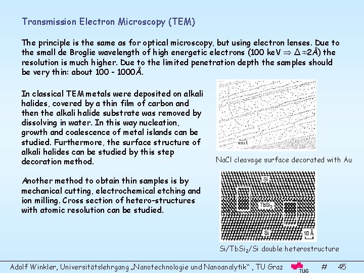
Transmission Electron Microscopy (TEM) The principle is the same as for optical microscopy, but using electron lenses. Due to the small de Broglie wavelength of high energetic electrons (100 ke. V Δ ≈2Å) the resolution is much higher. Due to the limited penetration depth the samples should be very thin: about 100 - 1000Å. In classical TEM metals were deposited on alkali halides, covered by a thin film of carbon and then the alkali halide substrate was removed by dissolving in water. In this way nucleation, growth and coalescence of metal islands can be studied. Furthermore, the surface structure of alkali halides can be studied by this step decoration method. Na. Cl cleavage surface decorated with Au Another method to obtain thin samples is by mechanical cutting, electrochemical etching and ion milling. Cross section of hetero-structures with atomic resolution can be studied. Si/Tb. Si 2/Si double heterostructure Adolf Winkler, Universitätslehrgang „Nanotechnologie und Nanoanalytik“ , TU Graz # 45

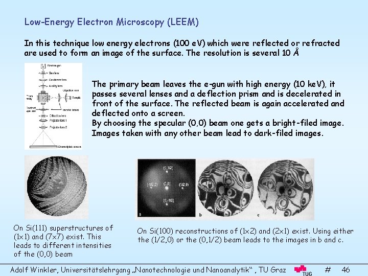
Low-Energy Electron Microscopy (LEEM) In this technique low energy electrons (100 e. V) which were reflected or refracted are used to form an image of the surface. The resolution is several 10 Å The primary beam leaves the e-gun with high energy (10 ke. V), it passes several lenses and a deflection prism and is decelerated in front of the surface. The reflected beam is again accelerated and deflected onto a screen. By choosing the specular (0, 0) beam one gets a bright-filed image. Images taken with any other beam lead to dark-filed images. On Si(111) superstructures of (1 x 1) and (7 x 7) exist. This leads to different intensities of the (0, 0) beam On Si(100) reconstructions of (1 x 2) and (2 x 1) exist. Using either the (1/2, 0) or the (0, 1/2) beam leads to the images in b and c. Adolf Winkler, Universitätslehrgang „Nanotechnologie und Nanoanalytik“ , TU Graz # 46

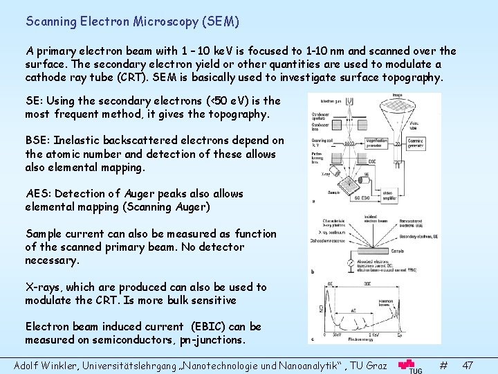
Scanning Electron Microscopy (SEM) A primary electron beam with 1 – 10 ke. V is focused to 1 -10 nm and scanned over the surface. The secondary electron yield or other quantities are used to modulate a cathode ray tube (CRT). SEM is basically used to investigate surface topography. SE: Using the secondary electrons (<50 e. V) is the most frequent method, it gives the topography. BSE: Inelastic backscattered electrons depend on the atomic number and detection of these allows also elemental mapping. AES: Detection of Auger peaks also allows elemental mapping (Scanning Auger) Sample current can also be measured as function of the scanned primary beam. No detector necessary. X-rays, which are produced can also be used to modulate the CRT. Is more bulk sensitive Electron beam induced current (EBIC) can be measured on semiconductors, pn-junctions. Adolf Winkler, Universitätslehrgang „Nanotechnologie und Nanoanalytik“ , TU Graz # 47

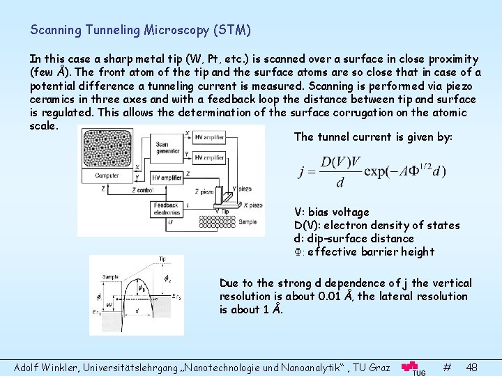
Scanning Tunneling Microscopy (STM) In this case a sharp metal tip (W, Pt, etc. ) is scanned over a surface in close proximity (few Å). The front atom of the tip and the surface atoms are so close that in case of a potential difference a tunneling current is measured. Scanning is performed via piezo ceramics in three axes and with a feedback loop the distance between tip and surface is regulated. This allows the determination of the surface corrugation on the atomic scale. The tunnel current is given by: V: bias voltage D(V): electron density of states d: dip-surface distance Φ: effective barrier height Due to the strong d dependence of j the vertical resolution is about 0. 01 Å, the lateral resolution is about 1 Å. Adolf Winkler, Universitätslehrgang „Nanotechnologie und Nanoanalytik“ , TU Graz # 48

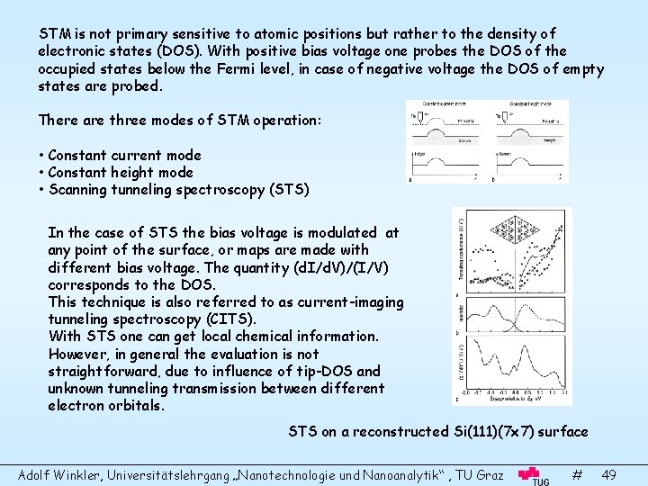
STM is not primary sensitive to atomic positions but rather to the density of electronic states (DOS). With positive bias voltage one probes the DOS of the occupied states below the Fermi level, in case of negative voltage the DOS of empty states are probed. There are three modes of STM operation: • Constant current mode • Constant height mode • Scanning tunneling spectroscopy (STS) In the case of STS the bias voltage is modulated at any point of the surface, or maps are made with different bias voltage. The quantity (d. I/d. V)/(I/V) corresponds to the DOS. This technique is also referred to as current-imaging tunneling spectroscopy (CITS). With STS one can get local chemical information. However, in general the evaluation is not straightforward, due to influence of tip-DOS and unknown tunneling transmission between different electron orbitals. STS on a reconstructed Si(111)(7 x 7) surface Adolf Winkler, Universitätslehrgang „Nanotechnologie und Nanoanalytik“ , TU Graz # 49

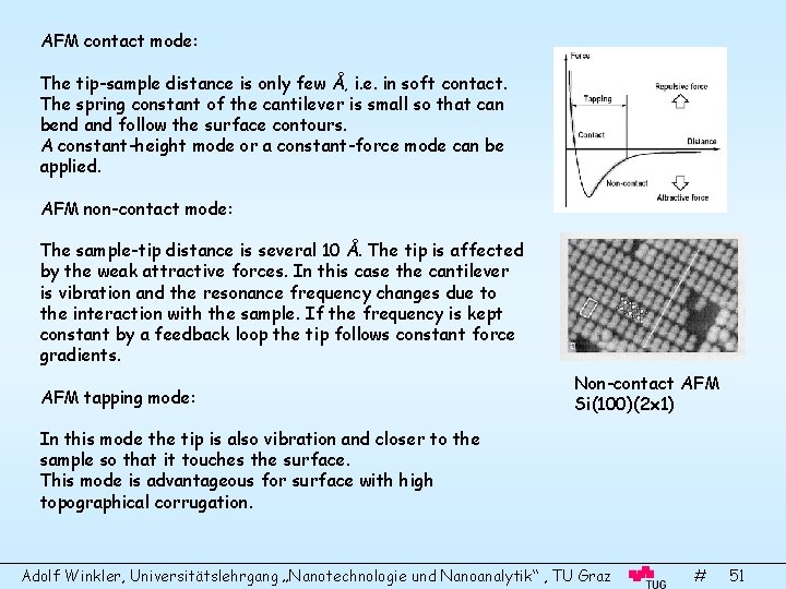
Atomic Force Microscopy (AFM) In AFM the force between tip and sample is measured. The interatomic force between tip and sample deflect a cantilever which carries the tip. In this case the morphology of conduction, semiconducting and insulating sample surfaces can be measured. There are several methods to measure the deflection of the cantilever: Use of an STM to measure the cantilever deflection Use of optical interferometry Deflection of a laser beam Measurement of capacitance between cantilever and a second electrode. Deflections of 10 -2 Å can be measured. The AFM can be used in three modes: • Contact mode • Non-contact mode • Tapping mode Adolf Winkler, Universitätslehrgang „Nanotechnologie und Nanoanalytik“ , TU Graz # 50

AFM contact mode: The tip-sample distance is only few Å, i. e. in soft contact. The spring constant of the cantilever is small so that can bend and follow the surface contours. A constant-height mode or a constant-force mode can be applied. AFM non-contact mode: The sample-tip distance is several 10 Å. The tip is affected by the weak attractive forces. In this case the cantilever is vibration and the resonance frequency changes due to the interaction with the sample. If the frequency is kept constant by a feedback loop the tip follows constant force gradients. AFM tapping mode: Non-contact AFM Si(100)(2 x 1) In this mode the tip is also vibration and closer to the sample so that it touches the surface. This mode is advantageous for surface with high topographical corrugation. Adolf Winkler, Universitätslehrgang „Nanotechnologie und Nanoanalytik“ , TU Graz # 51

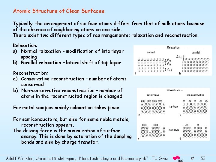
Atomic Structure of Clean Surfaces Typically, the arrangement of surface atoms differs from that of bulk atoms because of the absence of neighboring atoms on one side. There exist two different types of rearrangements: relaxation and reconstruction Relaxation: a) Normal relaxation – modification of interlayer spacing b) Parallel relaxation – lateral shift of top layer Reconstruction: a) Conservative reconstruction – number of atoms conserved b) Non-conservative reconstruction – number of atoms in the reconstructed region is changed For metal samples mainly relaxation takes place For semiconductors, but also for some noble metals, reconstruction appears. The driving force is the minimization of surface energy. This is done by saturation of the dangling bonds and also by charge transfer. Adolf Winkler, Universitätslehrgang „Nanotechnologie und Nanoanalytik“ , TU Graz # 52

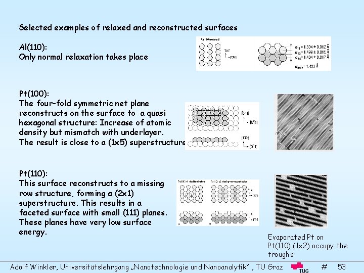
Selected examples of relaxed and reconstructed surfaces Al(110): Only normal relaxation takes place Pt(100): The four-fold symmetric net plane reconstructs on the surface to a quasi hexagonal structure: Increase of atomic density but mismatch with underlayer. The result is close to a (1 x 5) superstructure. Pt(110): This surface reconstructs to a missing row structure, forming a (2 x 1) superstructure. This results in a faceted surface with small (111) planes. These planes have very low surface energy. Evaporated Pt on Pt(110) (1 x 2) occupy the troughs Adolf Winkler, Universitätslehrgang „Nanotechnologie und Nanoanalytik“ , TU Graz # 53

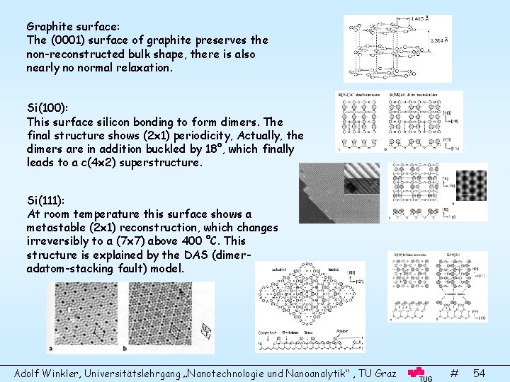
Graphite surface: The (0001) surface of graphite preserves the non-reconstructed bulk shape, there is also nearly no normal relaxation. Si(100): This surface silicon bonding to form dimers. The final structure shows (2 x 1) periodicity, Actually, the dimers are in addition buckled by 18°, which finally leads to a c(4 x 2) superstructure. Si(111): At room temperature this surface shows a metastable (2 x 1) reconstruction, which changes irreversibly to a (7 x 7) above 400 °C. This structure is explained by the DAS (dimeradatom-stacking fault) model. Adolf Winkler, Universitätslehrgang „Nanotechnologie und Nanoanalytik“ , TU Graz # 54

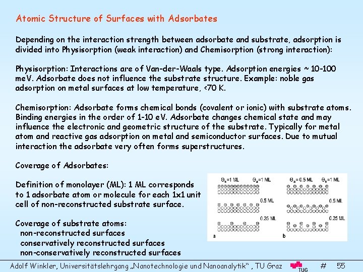
Atomic Structure of Surfaces with Adsorbates Depending on the interaction strength between adsorbate and substrate, adsorption is divided into Physisorption (weak interaction) and Chemisorption (strong interaction): Physisorption: Interactions are of Van-der-Waals type. Adsorption energies ~ 10 -100 me. V. Adsorbate does not influence the substrate structure. Example: noble gas adsorption on metal surfaces at low temperature, <70 K. Chemisorption: Adsorbate forms chemical bonds (covalent or ionic) with substrate atoms. Binding energies in the order of 1 -10 e. V. Adsorbate changes chemical state and may influence the electronic and geometric structure of the substrate. Typically for metal atom and reactive gas adsorption on metal and semiconductor surfaces. Due to mutual interaction the adsorbate very often forms superstructures. Coverage of Adsorbates: Definition of monolayer (ML): 1 ML corresponds to 1 adsorbate atom or molecule for each 1 x 1 unit cell of non-reconstructed substrate surface. Coverage of substrate atoms: non-reconstructed surfaces conservatively reconstructed surfaces non-conservatively reconstructed surfaces Adolf Winkler, Universitätslehrgang „Nanotechnologie und Nanoanalytik“ , TU Graz # 55

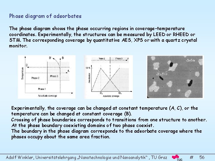
Phase diagram of adsorbates The phase diagram shows the phase occurring regions in coverage-temperature coordinates. Experimentally, the structures can be measured by LEED or RHEED or STM. The corresponding coverage by quantitative AES, XPS or with a quartz crystal monitor. Experimentally, the coverage can be changed at constant temperature (A, C), or the temperature can be changed at constant coverage (B). Crossing of phase boundaries corresponds to transitions from one structure to another. At the phase boundary coexisting domains of two phase coexist. The boundary in the phase diagram corresponds to the adsorbate coverage where the phases occupy about the same area fraction. Adolf Winkler, Universitätslehrgang „Nanotechnologie und Nanoanalytik“ , TU Graz # 56

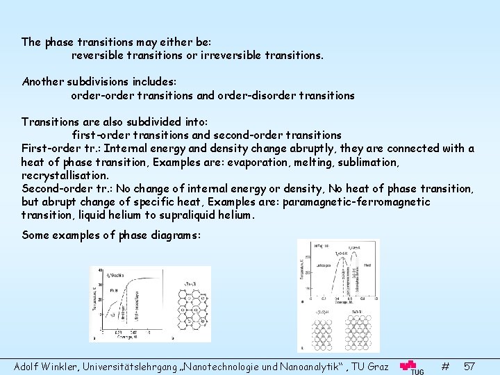
The phase transitions may either be: reversible transitions or irreversible transitions. Another subdivisions includes: order-order transitions and order-disorder transitions Transitions are also subdivided into: first-order transitions and second-order transitions First-order tr. : Internal energy and density change abruptly, they are connected with a heat of phase transition, Examples are: evaporation, melting, sublimation, recrystallisation. Second-order tr. : No change of internal energy or density, No heat of phase transition, but abrupt change of specific heat, Examples are: paramagnetic-ferromagnetic transition, liquid helium to supraliquid helium. Some examples of phase diagrams: Adolf Winkler, Universitätslehrgang „Nanotechnologie und Nanoanalytik“ , TU Graz # 57

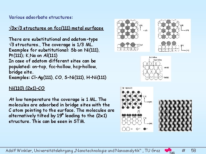
Various adsorbate structures: 3 x 3 structures on fcc(111) metal surfaces There are substitutional and adatom-type 3 structures. , The coverage is 1/3 ML. Examples for substitutional: Sb on Ni(111), Pt(111); K, Na on Al(111) In case of adatom different sites can be populated: on-top, fcc-hollow, hcp-hollow, bridge site. Examples: Cl-Ag(111), CO, S-Ni(111), H-Ni(111) Ni(110) (2 x 1)-CO At low temperature the coverage is 1 ML. The molecules are adsorbed in bridge sites with the C atom pointing to the surface. The molecules are alternatively tilted by 19° leading to the (2 x 1) structure. This can be seen in STM. Adolf Winkler, Universitätslehrgang „Nanotechnologie und Nanoanalytik“ , TU Graz # 58

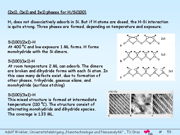
(2 x 1), (1 x 1) and 3 x 1) phases for H/Si(100) H 2 does not dissociatively adsorb in Si. But if H atoms are dosed, the H-Si interaction is quite strong. Three phases are formed, depending on temperature and exposure. Si(100)(2 x 1)-H At 400 °C and low exposure 1 ML forms. H forms monohydride with the Si dimers. Si(100)(1 x 1)-H At room temperature 2 ML can adsorb. The dimers are broken and dihydride forms with each Si atom. In this case many defects exist, due to formation of other phases, trihydride, gaseous silane, and monohydride (surface etching) Si(100)(3 x 1)-H This mixed structure is formed at intermediate temperature (110 °C). The structure consist of alternating monohydride and dihydride species. The coverage is 1. 33 ML. Adolf Winkler, Universitätslehrgang „Nanotechnologie und Nanoanalytik“ , TU Graz # 59

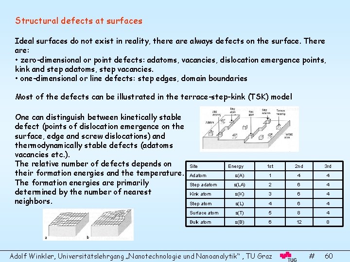
Structural defects at surfaces Ideal surfaces do not exist in reality, there always defects on the surface. There are: • zero-dimensional or point defects: adatoms, vacancies, dislocation emergence points, kink and step adatoms, step vacancies. • one-dimensional or line defects: step edges, domain boundaries Most of the defects can be illustrated in the terrace-step-kink (TSK) model One can distinguish between kinetically stable defect (points of dislocation emergence on the surface, edge and screw dislocations) and thermodynamically stable defects (adatoms vacancies etc. ). The relative number of defects depends on their formation energies and the temperature. The formation energies are primarily determined by the number of nearest neighbors. Site Energy 1 st 2 nd 3 rd Adatom (A) 1 4 4 Step adatom (LA) 2 6 4 Kink atom (K) 3 6 4 Step atom (L) 4 6 4 Surface atom (T) 5 8 4 Bulk atom (B) 6 12 8 Adolf Winkler, Universitätslehrgang „Nanotechnologie und Nanoanalytik“ , TU Graz # 60

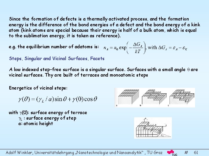
Since the formation of defects is a thermally activated process, and the formation energy is the difference of the bond energies of a defect and the bond energy of a kink atom (kink atoms are special because their energy is half of a bulk atom, which is equal to the sublimation energy, it is taken as reference). e. g. the equilibrium number of adatoms is: Steps, Singular and Vicinal Surfaces, Facets A low indexed step-free surface is a singular surface. Surfaces with a small angle are vicinal surfaces. Thy are built of terraces and monoatomic steps Energetics of vicinal steps: with (0): surface energy of terrace L : surface energy of step a: atomic height Adolf Winkler, Universitätslehrgang „Nanotechnologie und Nanoanalytik“ , TU Graz # 61

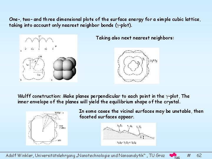
One-, two- and three dimensional plots of the surface energy for a simple cubic lattice, taking into account only nearest neighbor bonds ( -plot). Taking also next nearest neighbors: Wulff construction: Make planes perpendicular to each point in the -plot, The inner envelope of the planes will yield the equilibrium shape of the crystal. In some cases the vicinal surfaces may be unstable, then faceted surfaces appear. Adolf Winkler, Universitätslehrgang „Nanotechnologie und Nanoanalytik“ , TU Graz # 62

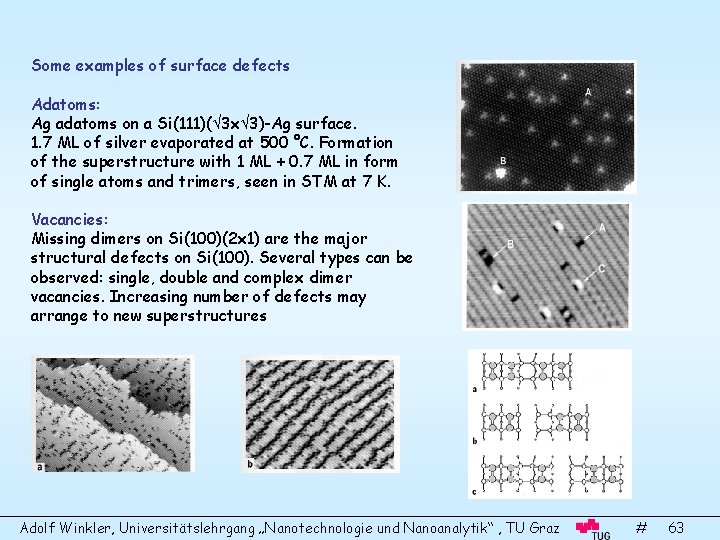
Some examples of surface defects Adatoms: Ag adatoms on a Si(111)( 3 x 3)-Ag surface. 1. 7 ML of silver evaporated at 500 °C. Formation of the superstructure with 1 ML + 0. 7 ML in form of single atoms and trimers, seen in STM at 7 K. Vacancies: Missing dimers on Si(100)(2 x 1) are the major structural defects on Si(100). Several types can be observed: single, double and complex dimer vacancies. Increasing number of defects may arrange to new superstructures Adolf Winkler, Universitätslehrgang „Nanotechnologie und Nanoanalytik“ , TU Graz # 63

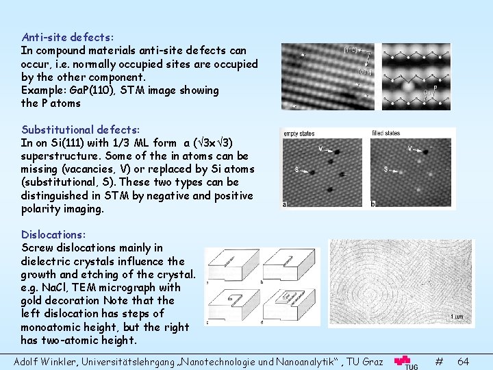
Anti-site defects: In compound materials anti-site defects can occur, i. e. normally occupied sites are occupied by the other component. Example: Ga. P(110), STM image showing the P atoms Substitutional defects: In on Si(111) with 1/3 ML form a ( 3 x 3) superstructure. Some of the in atoms can be missing (vacancies, V) or replaced by Si atoms (substitutional, S). These two types can be distinguished in STM by negative and positive polarity imaging. Dislocations: Screw dislocations mainly in dielectric crystals influence the growth and etching of the crystal. e. g. Na. Cl, TEM micrograph with gold decoration Note that the left dislocation has steps of monoatomic height, but the right has two-atomic height. Adolf Winkler, Universitätslehrgang „Nanotechnologie und Nanoanalytik“ , TU Graz # 64

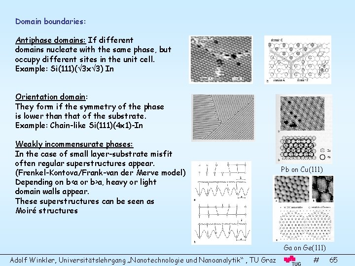
Domain boundaries: Antiphase domains: If different domains nucleate with the same phase, but occupy different sites in the unit cell. Example: Si(111)( 3 x 3) In Orientation domain: They form if the symmetry of the phase is lower than that of the substrate. Example: Chain-like Si(111)(4 x 1)-In Weakly incommensurate phases: In the case of small layer-substrate misfit often regular superstructures appear. (Frenkel-Kontova/Frank-van der Merve model) Depending on b<a or b>a, heavy or light domain walls appear. These superstructures can be seen as Moiré structures Pb on Cu(111) Ga on Ge(111) Adolf Winkler, Universitätslehrgang „Nanotechnologie und Nanoanalytik“ , TU Graz # 65

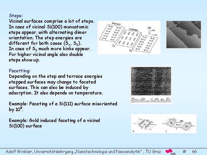
Steps: Vicinal surfaces comprise a lot of steps. In case of vicinal Si(100) monoatomic steps appear, with alternating dimer orientation. The step energies are different for both cases (SA, SB). In case of SB much more kinks appear. For higher vicinal angle also double steps show up. Facetting: Depending on the step and terrace energies stepped surfaces may change to faceted surfaces. This can also be induced by adsorption. It also depends on temperature. Example: Faceting of a Si(111) surface misoriented by 10°. Example: Gold induced faceting of a vicinal Si(100) surface Adolf Winkler, Universitätslehrgang „Nanotechnologie und Nanoanalytik“ , TU Graz # 66

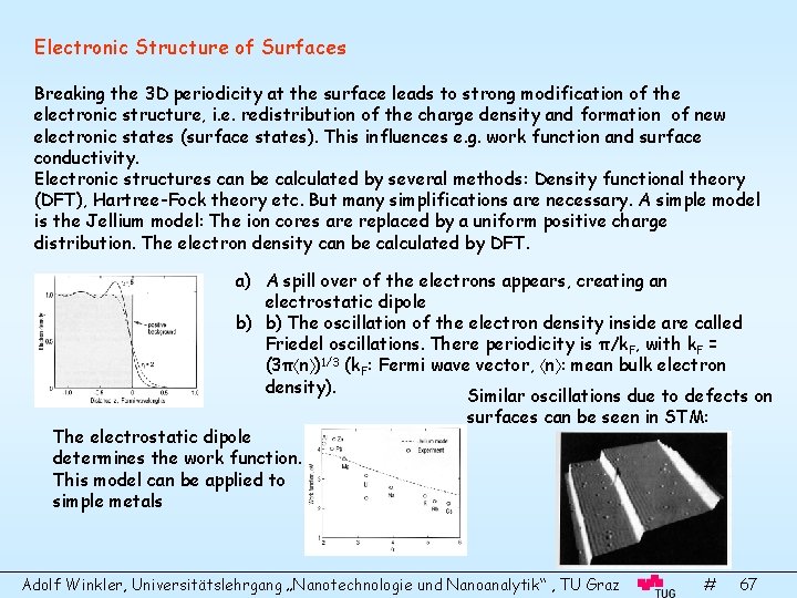
Electronic Structure of Surfaces Breaking the 3 D periodicity at the surface leads to strong modification of the electronic structure, i. e. redistribution of the charge density and formation of new electronic states (surface states). This influences e. g. work function and surface conductivity. Electronic structures can be calculated by several methods: Density functional theory (DFT), Hartree-Fock theory etc. But many simplifications are necessary. A simple model is the Jellium model: The ion cores are replaced by a uniform positive charge distribution. The electron density can be calculated by DFT. a) A spill over of the electrons appears, creating an electrostatic dipole b) b) The oscillation of the electron density inside are called Friedel oscillations. There periodicity is π/k. F, with k. F = (3π n )1/3 (k. F: Fermi wave vector, n : mean bulk electron density). Similar oscillations due to defects on The electrostatic dipole determines the work function. This model can be applied to simple metals surfaces can be seen in STM: Adolf Winkler, Universitätslehrgang „Nanotechnologie und Nanoanalytik“ , TU Graz # 67

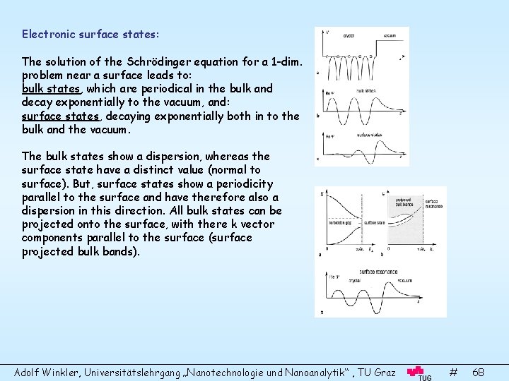
Electronic surface states: The solution of the Schrödinger equation for a 1 -dim. problem near a surface leads to: bulk states, which are periodical in the bulk and decay exponentially to the vacuum, and: surface states, decaying exponentially both in to the bulk and the vacuum. The bulk states show a dispersion, whereas the surface state have a distinct value (normal to surface). But, surface states show a periodicity parallel to the surface and have therefore also a dispersion in this direction. All bulk states can be projected onto the surface, with there k vector components parallel to the surface (surface projected bulk bands). Adolf Winkler, Universitätslehrgang „Nanotechnologie und Nanoanalytik“ , TU Graz # 68

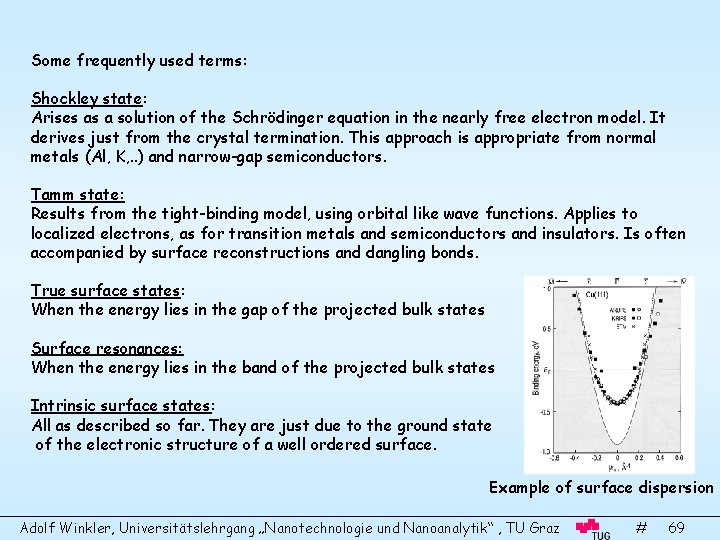
Some frequently used terms: Shockley state: Arises as a solution of the Schrödinger equation in the nearly free electron model. It derives just from the crystal termination. This approach is appropriate from normal metals (Al, K, . . ) and narrow-gap semiconductors. Tamm state: Results from the tight-binding model, using orbital like wave functions. Applies to localized electrons, as for transition metals and semiconductors and insulators. Is often accompanied by surface reconstructions and dangling bonds. True surface states: When the energy lies in the gap of the projected bulk states Surface resonances: When the energy lies in the band of the projected bulk states Intrinsic surface states: All as described so far. They are just due to the ground state of the electronic structure of a well ordered surface. Example of surface dispersion Adolf Winkler, Universitätslehrgang „Nanotechnologie und Nanoanalytik“ , TU Graz # 69

Extrinsic surface states: Are related to surface imperfections, like steps, defects, vacancies. There wave function is localized to the defect and no periodicity along the surface exists. Image potential surface states: Electrons on a surface induce a positive image potential in the solid. If the projected bulk states present a gap the electron cannot penetrate the bulk. It is confined (trapped) in front of the surface. Its energy levels are described by Rydberg-like series. Methods to investigate surface states: Angle resolved ultra violet photoemission (ARUPS): Probes the filled states. Measurement of photoelectron kinetic energy as function of angle. k-resolved inverse photoemission (KRIPS): Probes the unfilled states, by sending electrons to the surface and measuring energy of the emitted photons Scanning tunneling microscopy/spectroscopy (STM/STS): Probes either filled or unfilled states, depending on the polarity between tip and sample. STM probes directly the DOS. Measurement of Fridel oscillations as function of tip voltage directly yields the dispersion relation (E(kll)). Adolf Winkler, Universitätslehrgang „Nanotechnologie und Nanoanalytik“ , TU Graz # 70

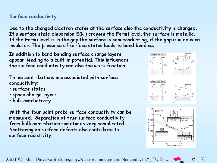
Surface conductivity Due to the changed electron states at the surface also the conductivity is changed. If a surface state dispersion E(kll) crosses the Fermi level, the surface is metallic. If the Fermi level is in the gap the surface is semiconducting, if the gap is wide is an insulator. The presence of surface states leads to bending: In addition to bending surface charge layers appear, leading to a built-in potential. This influences the surface conductivity and also the work function. Three contributions are associated with surface conductivity: • surface states • space charge layers • bulk conductivity With the four point probe surface conductivity can be measured. Separation of true surface conductivity from bulk contribution sometimes very complicated. Scattering on surface defects also contribute to surface resistivity. Adolf Winkler, Universitätslehrgang „Nanotechnologie und Nanoanalytik“ , TU Graz # 71

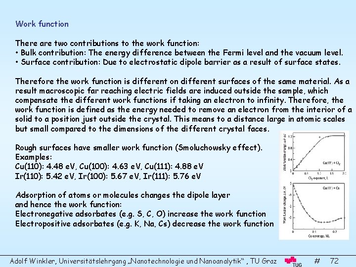
Work function There are two contributions to the work function: • Bulk contribution: The energy difference between the Fermi level and the vacuum level. • Surface contribution: Due to electrostatic dipole barrier as a result of surface states. Therefore the work function is different on different surfaces of the same material. As a result macroscopic far reaching electric fields are induced outside the sample, which compensate the different work functions if taking an electron to infinity. Therefore, the work function is defined as the energy needed to remove an electron from the interior of a solid to a position just outside the crystal. This means to a distance large in atomic scales but small compared to the dimensions of the different crystal faces. Rough surfaces have smaller work function (Smoluchowsky effect). Examples: Cu(110): 4. 48 e. V, Cu(100): 4. 63 e. V, Cu(111): 4. 88 e. V Ir(110): 5. 42 e. V, Ir(100): 5. 67 e. V, Ir(111): 5. 76 e. V Adsorption of atoms or molecules changes the dipole layer and hence the work function: Electronegative adsorbates (e. g. S, C, O) increase the work function Electropositive adsorbates (e. g. K, Na, Cs) decrease the work function Adolf Winkler, Universitätslehrgang „Nanotechnologie und Nanoanalytik“ , TU Graz # 72

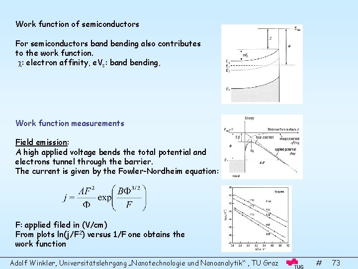
Work function of semiconductors For semiconductors band bending also contributes to the work function. : electron affinity, e. Vs: band bending, Work function measurements Field emission: A high applied voltage bends the total potential and electrons tunnel through the barrier. The current is given by the Fowler-Nordheim equation: F: applied filed in (V/cm) From plots ln(j/F 2) versus 1/F one obtains the work function Adolf Winkler, Universitätslehrgang „Nanotechnologie und Nanoanalytik“ , TU Graz # 73

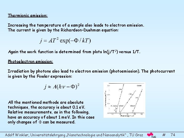
Thermionic emission: Increasing the temperature of a sample also leads to electron emission. The current is given by the Richardson-Dushman equation: Again the work function is determined from plots ln(j/T 2) versus 1/T. Photoelectron emission: Irradiation by photons also lead to electron emission (photoemission). The photocurrent is given by the Fowler expression: All the mentioned methods are absolute techniques, the accuracy is about 0. 1 e. V. Relative measurements, as in the following, have an accuracy of about 1 me. V. In this case only changes of can be measured. Adolf Winkler, Universitätslehrgang „Nanotechnologie und Nanoanalytik“ , TU Graz # 74

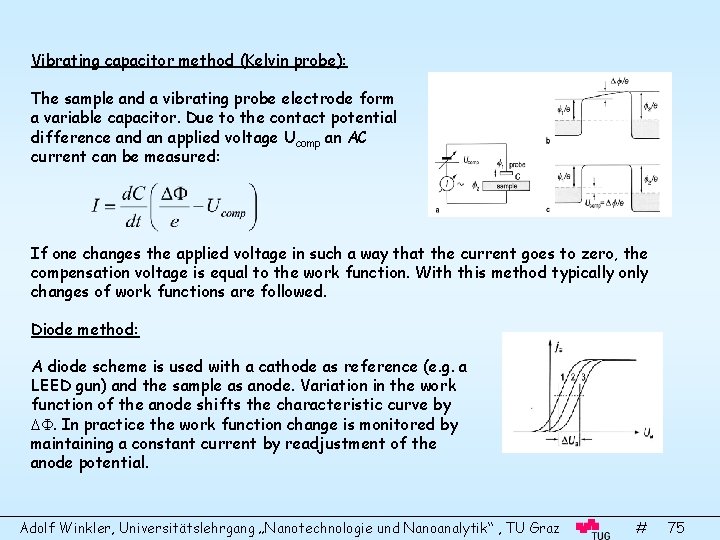
Vibrating capacitor method (Kelvin probe): The sample and a vibrating probe electrode form a variable capacitor. Due to the contact potential difference and an applied voltage Ucomp an AC current can be measured: If one changes the applied voltage in such a way that the current goes to zero, the compensation voltage is equal to the work function. With this method typically only changes of work functions are followed. Diode method: A diode scheme is used with a cathode as reference (e. g. a LEED gun) and the sample as anode. Variation in the work function of the anode shifts the characteristic curve by . In practice the work function change is monitored by maintaining a constant current by readjustment of the anode potential. Adolf Winkler, Universitätslehrgang „Nanotechnologie und Nanoanalytik“ , TU Graz # 75

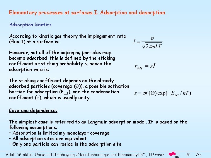
Elementary processes at surfaces I: Adsorption and desorption Adsorption kinetics According to kinetic gas theory the impingement rate (flux I) at a surface is: However, not all of the impinging particles may become adsorbed, this is defined by the sticking coefficient or sticking probability s, hence the adsorption rate is: The sticking coefficient depends on the already adsorbed particles (coverage ( )), a possible activation barrier for adsorption (Eact), and the condensation coefficient ( ), which is usually unity. Coverage dependence: The simplest case is referred to as Langmuir adsorption model. It is based on the following assumptions: • Adsorption is limited my monolayer coverage • All adsorption sites are equivalent • Only one particle can reside in the adsorption site Adolf Winkler, Universitätslehrgang „Nanotechnologie und Nanoanalytik“ , TU Graz # 76

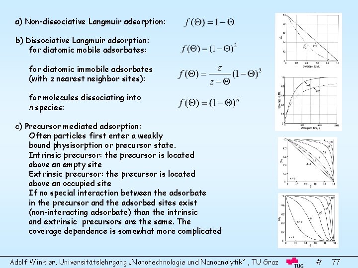
a) Non-dissociative Langmuir adsorption: b) Dissociative Langmuir adsorption: for diatomic mobile adsorbates: for diatomic immobile adsorbates (with z nearest neighbor sites): for molecules dissociating into n species: c) Precursor mediated adsorption: Often particles first enter a weakly bound physisorption or precursor state. Intrinsic precursor: the precursor is located above an empty site Extrinsic precursor: the precursor is located above an occupied site If no special interaction between the adsorbate in the precursor and the adsorbed sites exist (non-interacting adsorbate) than the intrinsic and extrinsic precursors are the same. The coverage dependence is somewhat more complicated Adolf Winkler, Universitätslehrgang „Nanotechnologie und Nanoanalytik“ , TU Graz # 77

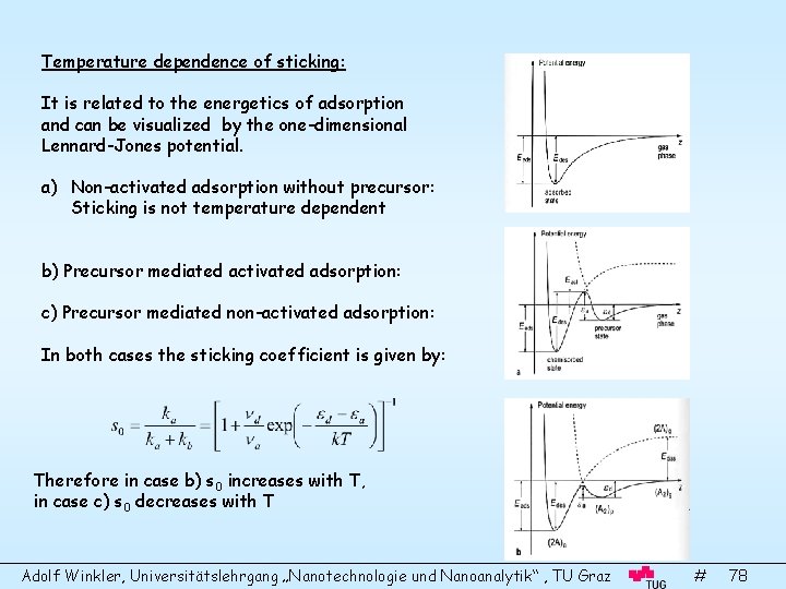
Temperature dependence of sticking: It is related to the energetics of adsorption and can be visualized by the one-dimensional Lennard-Jones potential. a) Non-activated adsorption without precursor: Sticking is not temperature dependent b) Precursor mediated activated adsorption: c) Precursor mediated non-activated adsorption: In both cases the sticking coefficient is given by: Therefore in case b) s 0 increases with T, in case c) s 0 decreases with T Adolf Winkler, Universitätslehrgang „Nanotechnologie und Nanoanalytik“ , TU Graz # 78

Angular and Kinetic energy dependence In case of activated adsorption, the kinetic energy of the impinging molecule helps to surmount the barrier. S increases with Ekin. In case of precursor adsorption the accommodation into the precursor state is relevant. Accommodation typically decreases with increasing kinetic energy. Therefore in this case S decreases with increasing Ekin. In case of direct adsorption without activation barriers or precursors the sticking may by independent of Ekin. Since in many cases only the normal energy is relevant (E = E·cos 2 ), it follows that the angular dependence of sticking is closely related to the energy dependence. For energy independent sticking it is also angle independent. But by convention this is described as cosine dependent. S( ) = S 0 cos. (Due to the geometric decrease of the impinging flux per surface unit!). In all other cases the angular dependence can be roughly described by a cosn function, with n = 1 for S(E) constant (direct unactivated adsorption) n > 1 for S(E) increasing with E (activated adsorption) n < 1 for S(E) decreasing with E (precursor adsorption or steering) Adolf Winkler, Universitätslehrgang „Nanotechnologie und Nanoanalytik“ , TU Graz # 79

Thermal Desorption If adsorbed molecules gain energy by increasing the substrate temperature they can escape the adsorption potential due to increased thermal vibrations. Most frequently the desorption rate is expressed for non-interacting particles by the Polanyi-Wigner equation: Kinetic order n: 0. order: If desorption at a given temperature is not coverage dependent, e. g. for multilayer film desorption (evaporation) or if a 2 D two-phase system exists on the surface 1. order: If single atoms or molecules desorb directly 2. order: If two atoms recombine during desorption Adolf Winkler, Universitätslehrgang „Nanotechnologie und Nanoanalytik“ , TU Graz # 80

Desorption energy: In case of activated adsorption: Edes = Eads + Eact In case of non-activated adsorption: Edes = Eact In case of particle interaction (attractive or repulsive) Edes is coverage dependent Angular and kinetic energy dependence: Adsorption and desorption is closely related by the Principle of Detailed Balancing: This means, e. g. for activated adsorption, if the adsorption probability is larger for high energetic particles, also in the desorption flux high energetic particles are abundant. This leads to a hyperhermal flux. Also, if sticking at normal incidence is higher also the desorption flux is peaked towards the surface normal (often expressed with cosn , with n>1) Adolf Winkler, Universitätslehrgang „Nanotechnologie und Nanoanalytik“ , TU Graz # 81

Thermal desorption spectroscopy: For the determination of Edes, n and two experimental methods are usually employed: Isothermal desorption spectroscopy (ITDS): First the temperature is raised rapidly to a fix value and then held constant. From the change of the coverage and/or the desorption rate one can evaluate all the interesting parameters. Adolf Winkler, Universitätslehrgang „Nanotechnologie und Nanoanalytik“ , TU Graz # 82

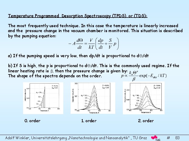
Temperature Programmed Desorption Spectroscopy (TPDS), or (TDS): The most frequently used technique. In this case the temperature is linearly increased and the pressure change in the vacuum chamber is monitored. This situation is described by the pumping equation: a) If the pumping speed is very low, then dp/dt is proportional to d /dt b) If S is high, the p is proportional to d /dt. This is the commonly used regime. If the linear heating rate is , then the pressure change is given by: The shape of the spectra depends on the order. 0. order 1. order 2. order Adolf Winkler, Universitätslehrgang „Nanotechnologie und Nanoanalytik“ , TU Graz # 83

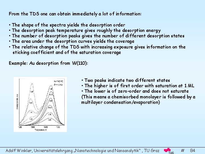
From the TDS one can obtain immediately a lot of information: • The shape of the spectra yields the desorption order • The desorption peak temperature gives roughly the desorption energy • The number of desorption peaks gives the number of different desorption states • The area under the desorption curves yields the coverage • The relative change of the TDS with increasing exposure gives information on the sticking coefficient and of the saturation coverage Example: Au desorption from W(110): • Two peaks indicate two different states • The higher is of first order with saturation at 1 ML • The lower is of zero-order and does not saturate (This means a chemisorbed monolayer is followed by a multilayer condensation/evaporation) Adolf Winkler, Universitätslehrgang „Nanotechnologie und Nanoanalytik“ , TU Graz # 84

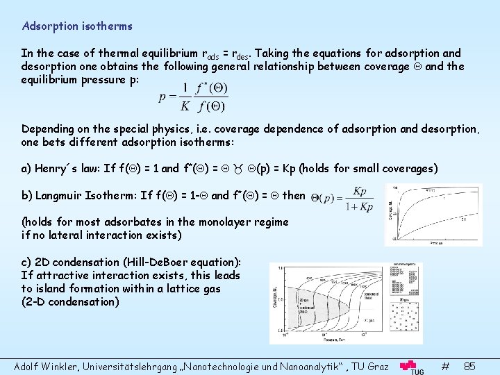
Adsorption isotherms In the case of thermal equilibrium rads = rdes. Taking the equations for adsorption and desorption one obtains the following general relationship between coverage and the equilibrium pressure p: Depending on the special physics, i. e. coverage dependence of adsorption and desorption, one bets different adsorption isotherms: a) Henry´s law: If f( ) = 1 and f*( ) = (p) = Kp (holds for small coverages) b) Langmuir Isotherm: If f( ) = 1 - and f*( ) = then (holds for most adsorbates in the monolayer regime if no lateral interaction exists) c) 2 D condensation (Hill-De. Boer equation): If attractive interaction exists, this leads to island formation within a lattice gas (2 -D condensation) Adolf Winkler, Universitätslehrgang „Nanotechnologie und Nanoanalytik“ , TU Graz # 85

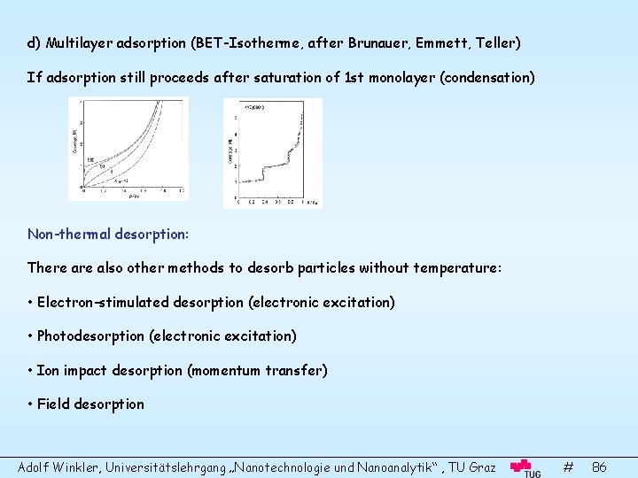
d) Multilayer adsorption (BET-Isotherme, after Brunauer, Emmett, Teller) If adsorption still proceeds after saturation of 1 st monolayer (condensation) Non-thermal desorption: There also other methods to desorb particles without temperature: • Electron-stimulated desorption (electronic excitation) • Photodesorption (electronic excitation) • Ion impact desorption (momentum transfer) • Field desorption Adolf Winkler, Universitätslehrgang „Nanotechnologie und Nanoanalytik“ , TU Graz # 86

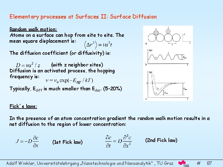
Elementary processes at Surfaces II: Surface Diffusion Random walk motion: Atoms on a surface can hop from site to site. The mean square displacement is: The diffusion coefficient (or diffusivity) is: (with z neighbor sites) Diffusion is an activated process, the hopping frequency is: Typically, Ediff is much smaller than Edes. (5 -20%) Fick´s laws: In the presence of an atom concentration gradient the random walk motion results in a net diffusion to the region of lower concentration: (1 st Fick law) (2 nd Fick law) Adolf Winkler, Universitätslehrgang „Nanotechnologie und Nanoanalytik“ , TU Graz # 87

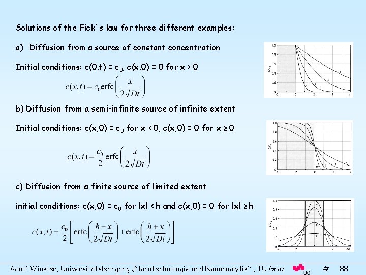
Solutions of the Fick´s law for three different examples: a) Diffusion from a source of constant concentration Initial conditions: c(0, t) = c 0, c(x, 0) = 0 for x > 0 b) Diffusion from a semi-infinite source of infinite extent Initial conditions: c(x, 0) = c 0 for x < 0, c(x, 0) = 0 for x ≥ 0 c) Diffusion from a finite source of limited extent initial conditions: c(x, 0) = c 0 for lxl < h and c(x, 0) = 0 for lxl ≥ h Adolf Winkler, Universitätslehrgang „Nanotechnologie und Nanoanalytik“ , TU Graz # 88

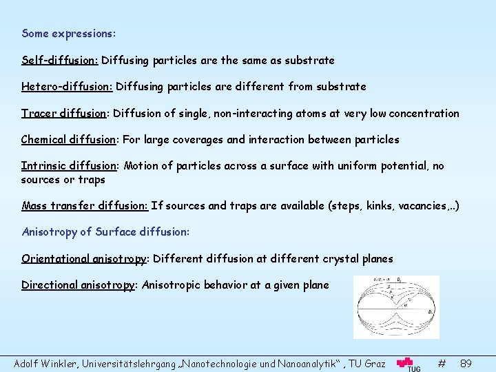
Some expressions: Self-diffusion: Diffusing particles are the same as substrate Hetero-diffusion: Diffusing particles are different from substrate Tracer diffusion: Diffusion of single, non-interacting atoms at very low concentration Chemical diffusion: For large coverages and interaction between particles Intrinsic diffusion: Motion of particles across a surface with uniform potential, no sources or traps Mass transfer diffusion: If sources and traps are available (steps, kinks, vacancies, . . ) Anisotropy of Surface diffusion: Orientational anisotropy: Different diffusion at different crystal planes Directional anisotropy: Anisotropic behavior at a given plane Adolf Winkler, Universitätslehrgang „Nanotechnologie und Nanoanalytik“ , TU Graz # 89

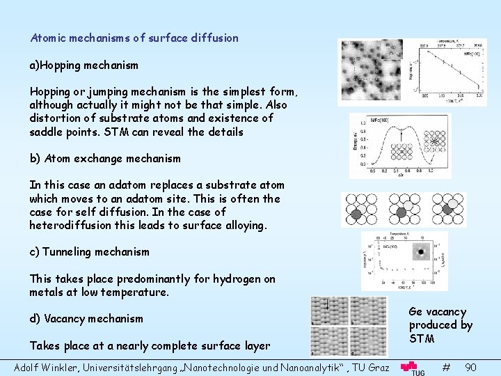
Atomic mechanisms of surface diffusion a)Hopping mechanism Hopping or jumping mechanism is the simplest form, although actually it might not be that simple. Also distortion of substrate atoms and existence of saddle points. STM can reveal the details b) Atom exchange mechanism In this case an adatom replaces a substrate atom which moves to an adatom site. This is often the case for self diffusion. In the case of heterodiffusion this leads to surface alloying. c) Tunneling mechanism This takes place predominantly for hydrogen on metals at low temperature. d) Vacancy mechanism Takes place at a nearly complete surface layer Adolf Winkler, Universitätslehrgang „Nanotechnologie und Nanoanalytik“ , TU Graz Ge vacancy produced by STM # 90

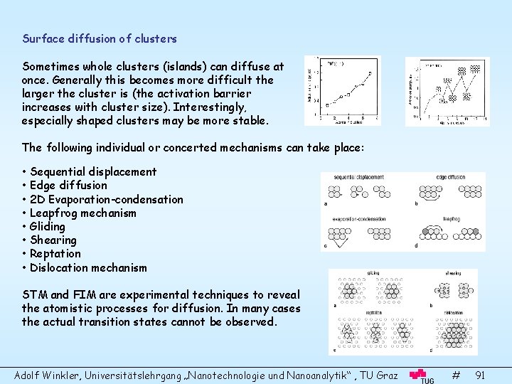
Surface diffusion of clusters Sometimes whole clusters (islands) can diffuse at once. Generally this becomes more difficult the larger the cluster is (the activation barrier increases with cluster size). Interestingly, especially shaped clusters may be more stable. The following individual or concerted mechanisms can take place: • Sequential displacement • Edge diffusion • 2 D Evaporation-condensation • Leapfrog mechanism • Gliding • Shearing • Reptation • Dislocation mechanism STM and FIM are experimental techniques to reveal the atomistic processes for diffusion. In many cases the actual transition states cannot be observed. Adolf Winkler, Universitätslehrgang „Nanotechnologie und Nanoanalytik“ , TU Graz # 91

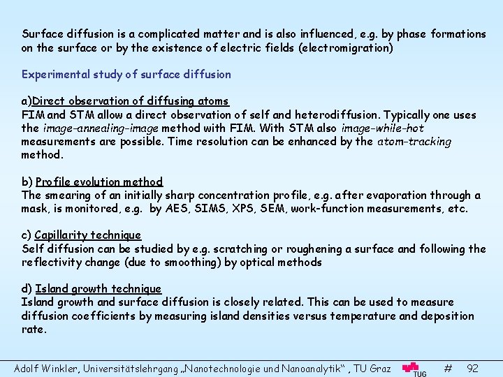
Surface diffusion is a complicated matter and is also influenced, e. g. by phase formations on the surface or by the existence of electric fields (electromigration) Experimental study of surface diffusion a)Direct observation of diffusing atoms FIM and STM allow a direct observation of self and heterodiffusion. Typically one uses the image-annealing-image method with FIM. With STM also image-while-hot measurements are possible. Time resolution can be enhanced by the atom-tracking method. b) Profile evolution method The smearing of an initially sharp concentration profile, e. g. after evaporation through a mask, is monitored, e. g. by AES, SIMS, XPS, SEM, work-function measurements, etc. c) Capillarity technique Self diffusion can be studied by e. g. scratching or roughening a surface and following the reflectivity change (due to smoothing) by optical methods d) Island growth technique Island growth and surface diffusion is closely related. This can be used to measure diffusion coefficients by measuring island densities versus temperature and deposition rate. Adolf Winkler, Universitätslehrgang „Nanotechnologie und Nanoanalytik“ , TU Graz # 92

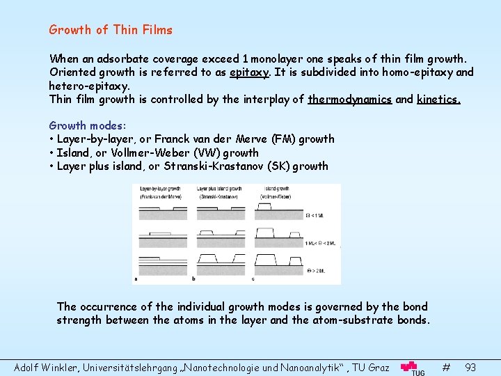
Growth of Thin Films When an adsorbate coverage exceed 1 monolayer one speaks of thin film growth. Oriented growth is referred to as epitaxy. It is subdivided into homo-epitaxy and hetero-epitaxy. Thin film growth is controlled by the interplay of thermodynamics and kinetics. Growth modes: • Layer-by-layer, or Franck van der Merve (FM) growth • Island, or Vollmer-Weber (VW) growth • Layer plus island, or Stranski-Krastanov (SK) growth The occurrence of the individual growth modes is governed by the bond strength between the atoms in the layer and the atom-substrate bonds. Adolf Winkler, Universitätslehrgang „Nanotechnologie und Nanoanalytik“ , TU Graz # 93

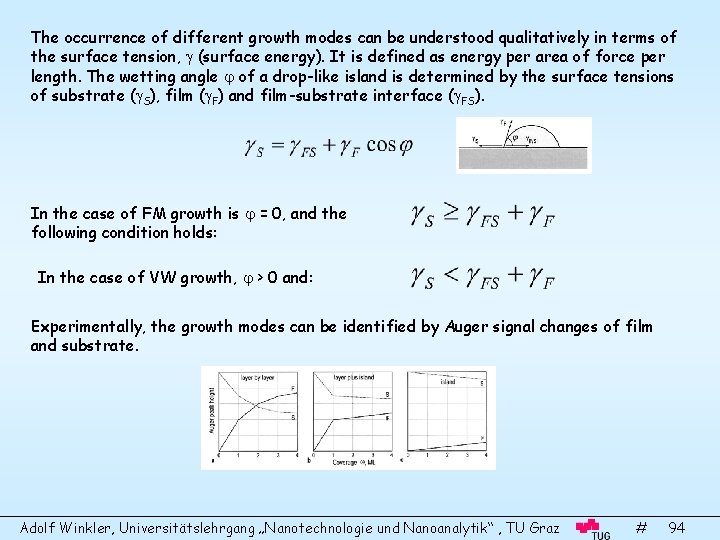
The occurrence of different growth modes can be understood qualitatively in terms of the surface tension, (surface energy). It is defined as energy per area of force per length. The wetting angle of a drop-like island is determined by the surface tensions of substrate ( S), film ( F) and film-substrate interface ( FS). In the case of FM growth is = 0, and the following condition holds: In the case of VW growth, > 0 and: Experimentally, the growth modes can be identified by Auger signal changes of film and substrate. Adolf Winkler, Universitätslehrgang „Nanotechnologie und Nanoanalytik“ , TU Graz # 94

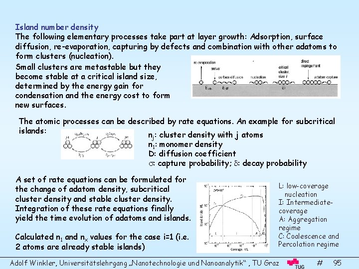
Island number density The following elementary processes take part at layer growth: Adsorption, surface diffusion, re-evaporation, capturing by defects and combination with other adatoms to form clusters (nucleation). Small clusters are metastable but they become stable at a critical island size, determined by the energy gain for condensation and the energy cost to form new surfaces. The atomic processes can be described by rate equations. An example for subcritical islands: n : cluster density with j atoms j n 1: monomer density D: diffusion coefficient : capture probability; : decay probability A set of rate equations can be formulated for the change of adatom density, subcritical cluster density and stable cluster density. Integration of these rate equations finally yield the time evolution of adatoms and islands. Calculated n 1 and nx values for the case i=1 (i. e. 2 atoms are already stable islands) L: low-coverage nucleation I: Intermediatecoverage A: Aggregation regime C: Coalescence and Percolation regime Adolf Winkler, Universitätslehrgang „Nanotechnologie und Nanoanalytik“ , TU Graz # 95

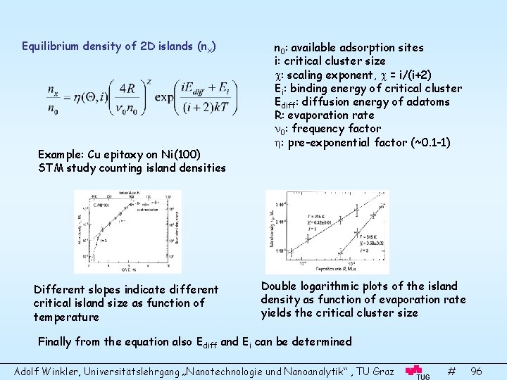
Equilibrium density of 2 D islands (nx) Example: Cu epitaxy on Ni(100) STM study counting island densities Different slopes indicate different critical island size as function of temperature n 0: available adsorption sites i: critical cluster size : scaling exponent, = i/(i+2) Ei: binding energy of critical cluster Ediff: diffusion energy of adatoms R: evaporation rate 0: frequency factor : pre-exponential factor (~0. 1 -1) Double logarithmic plots of the island density as function of evaporation rate yields the critical cluster size Finally from the equation also Ediff and Ei can be determined Adolf Winkler, Universitätslehrgang „Nanotechnologie und Nanoanalytik“ , TU Graz # 96

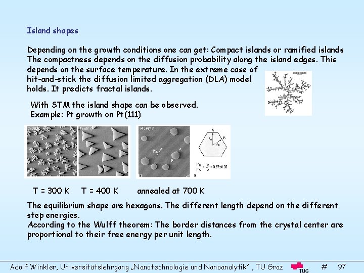
Island shapes Depending on the growth conditions one can get: Compact islands or ramified islands The compactness depends on the diffusion probability along the island edges. This depends on the surface temperature. In the extreme case of hit-and-stick the diffusion limited aggregation (DLA) model holds. It predicts fractal islands. With STM the island shape can be observed. Example: Pt growth on Pt(111) T = 300 K T = 400 K annealed at 700 K The equilibrium shape are hexagons. The different length depend on the different step energies. According to the Wulff theorem: The border distances from the crystal center are proportional to their free energy per unit length. Adolf Winkler, Universitätslehrgang „Nanotechnologie und Nanoanalytik“ , TU Graz # 97

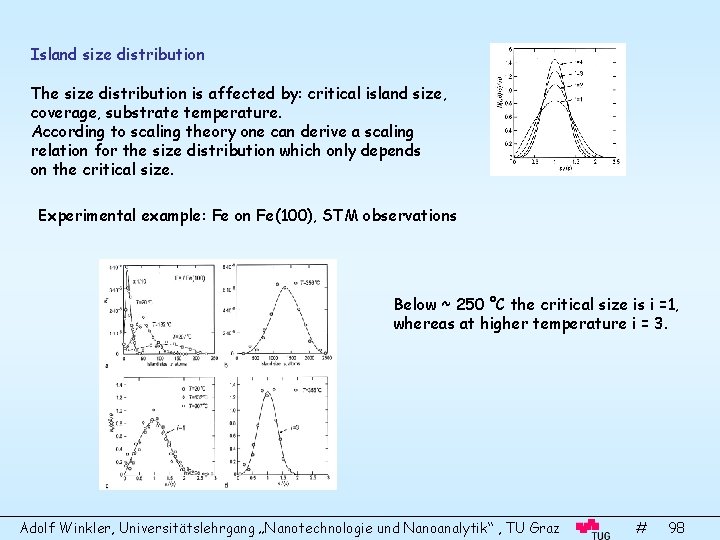
Island size distribution The size distribution is affected by: critical island size, coverage, substrate temperature. According to scaling theory one can derive a scaling relation for the size distribution which only depends on the critical size. Experimental example: Fe on Fe(100), STM observations Below ~ 250 °C the critical size is i =1, whereas at higher temperature i = 3. Adolf Winkler, Universitätslehrgang „Nanotechnologie und Nanoanalytik“ , TU Graz # 98

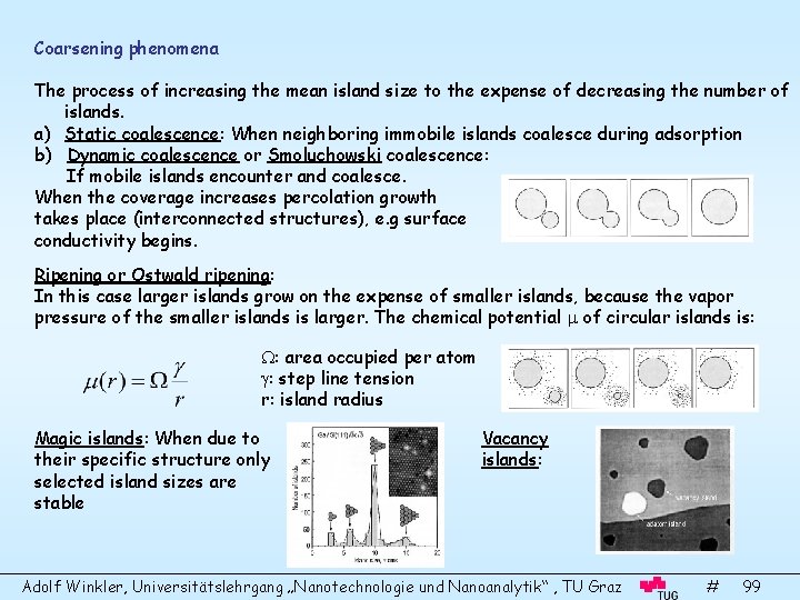
Coarsening phenomena The process of increasing the mean island size to the expense of decreasing the number of islands. a) Static coalescence: When neighboring immobile islands coalesce during adsorption b) Dynamic coalescence or Smoluchowski coalescence: If mobile islands encounter and coalesce. When the coverage increases percolation growth takes place (interconnected structures), e. g surface conductivity begins. Ripening or Ostwald ripening: In this case larger islands grow on the expense of smaller islands, because the vapor pressure of the smaller islands is larger. The chemical potential of circular islands is: : area occupied per atom : step line tension r: island radius Magic islands: When due to their specific structure only selected island sizes are stable Vacancy islands: Adolf Winkler, Universitätslehrgang „Nanotechnologie und Nanoanalytik“ , TU Graz # 99

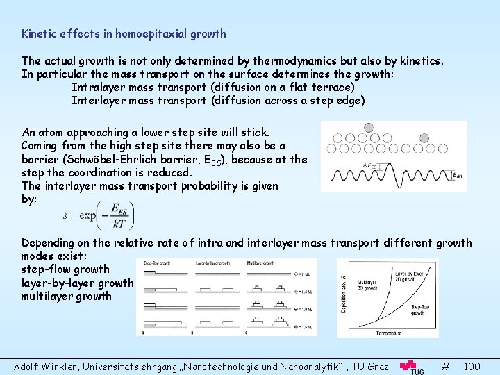
Kinetic effects in homoepitaxial growth The actual growth is not only determined by thermodynamics but also by kinetics. In particular the mass transport on the surface determines the growth: Intralayer mass transport (diffusion on a flat terrace) Interlayer mass transport (diffusion across a step edge) An atom approaching a lower step site will stick. Coming from the high step site there may also be a barrier (Schwöbel-Ehrlich barrier, EES), because at the step the coordination is reduced. The interlayer mass transport probability is given by: Depending on the relative rate of intra and interlayer mass transport different growth modes exist: step-flow growth layer-by-layer growth multilayer growth Adolf Winkler, Universitätslehrgang „Nanotechnologie und Nanoanalytik“ , TU Graz # 100

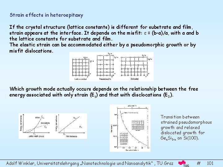
Strain effects in heteroepitaxy If the crystal structure (lattice constants) is different for substrate and film, strain appears at the interface. It depends on the misfit: = (b-a)/a, with a and b the lattice constants for substrate and film. The elastic strain can be accommodated either by a pseudomorphic growth or by misfit dislocations. Which growth mode actually occurs depends on the relationship between the free energy associated with only strain (E ) and that with disclocations (ED). Transition between strained pseudomorphous growth and relaxed dislocated growth for Gex. Si 1 -x on Si(100). Adolf Winkler, Universitätslehrgang „Nanotechnologie und Nanoanalytik“ , TU Graz # 101

Thin film growth techniques a) Molecular beam epitaxy: Molecules or atoms are evaporated onto a surface under UHV conditions. Sample at elevated temperature. Small flux. High quality layers. Monitoring of film structure by RHEED. b) Solid phase epitaxy: First deposition of amorphous layer at medium temperature, then annealing c) Chemical beam epitaxy: In this case material is supplied to the surface by gaseous compounds at rather high pressure. Substrate at high temperature, compounds dissociate (Chemical vapor deposition (CVD)). e. g. Si. H 4, As. H 3, Trimethyl gallium). If growth is performed at UHV conditions, then it is called metal-organic MBE (MOMBE) or chemical beam epitaxy (CBE) Adolf Winkler, Universitätslehrgang „Nanotechnologie und Nanoanalytik“ , TU Graz # 102

Surfactant mediated growth Certain impurities on a surface may change the growth modes. These impurities are called surfactants. The classical definition is, that a surfactant lowers surface tension and thereby increases the spreading and wetting of the film. Actually, it turns out that rather a modification of the kinetics takes place rather then a change of the energetics. Fort example the adatom diffusivity on the terraces might be influenced, the number of nucleation centers can be changed, the Schwöbel barrier may be changed etc. The classical example is the growth of Ge on Si(111). On the bare surface there is a Stranski-Krastanov growth. With 1 ML Sb as a surfactant the film grows in a layer-by-layer fashion. Another example is the influence of H on Si(111) on the growth of Ag. Adolf Winkler, Universitätslehrgang „Nanotechnologie und Nanoanalytik“ , TU Graz # 103

Atomic Manipulation and Nanostructure Formation Typically nanostructures have dimensions of 1 -10 (100) nm. They can be produced either by atomic manipulation or self-organization. nanostructures are characterized by surface dominated effects and quantum size effects. A typical surface dominated effect is the decrease of the melting temperature with decreasing cluster size ( T ~ 1/L). A typical quantum size effect is the discretisation of the energy levels (DOS). • Quantum films are confined in one spatial direction • Quantum wires are confined in two dimensions • Quantum dots are confined in three dimensions Short overview of the density of electronic states (DOS) for 3 D, 2 D, 1 D and 0 D free electron gases: For 3 D: All the possible states are the solution of the Schrödinger equation: standing waves in form of: with components of k: The energy of this state is: Adolf Winkler, Universitätslehrgang „Nanotechnologie und Nanoanalytik“ , TU Graz # 104

Each allowed state occupies a volume in k-space of (2π/L) 3, The volume of a spherical shell with radius k and thickness dk is 4πk 2 dk. Then the number of states in this volume are (taking into account two valus of spin): With it follows the DOS per unit volume and energy E : For 2 D: The procedure is similar, now each state occupies an area of (2π/L) 2, and the area of an annulus is 2πkdk. This leads to a DOS for the ground state: The energy accompanied with the k-vector in the third direction is quantized. The total DOS is the sum of all DOS for each discrete energy levels due to normal confinement. with the Heaviside function H H = 0 for E < En and H = 1 for E ≥ En Adolf Winkler, Universitätslehrgang „Nanotechnologie und Nanoanalytik“ , TU Graz # 105

For 1 D: The DOS takes the following form For 0 D finally all energy states exist only as discrete levels (like for an atom) Adolf Winkler, Universitätslehrgang „Nanotechnologie und Nanoanalytik“ , TU Graz # 106

Atomic manipulation with STM Lateral atomic displacements, surface atom extraction and single atom deposition can be performed with STM Lateral atomic displacement: Can be induced by interatomic forces (atom sliding) or electrostatic fields (field assisted diffusion). Xe on Ni(110) Fe on Cu(111) Different examples of atom arrangements by STM manipulation Adolf Winkler, Universitätslehrgang „Nanotechnologie und Nanoanalytik“ , TU Graz # 107

Field assisted diffusion: In the case of adsorbed particles they may form a static dipole and even an induced dipole in the inhomogeneous field E(r) around an STM tip. The total dipole moment is: p = p 0 + E; the potential energy is U(r) = - p 0 E(r) E 2(r)/2. Static dipoles may be attracted or repulsed by the STM field, induced dipoles are always attracted. Atomic extraction: Atoms can be removed from the surface and transferred to the tip by: strong interatomic interactions (touching the surface), filed evaporation (by high fields, several V), electron-stimulated desorption (due to electron current between tip and sample). Atom deposition: Single atoms can be deposited by the same method (touching). Small clusters can also be deposited, with the z-pulse method or the V pulse method. Adolf Winkler, Universitätslehrgang „Nanotechnologie und Nanoanalytik“ , TU Graz # 108

Self-Organization of Nanostructures In some cases evaporated material arranges in special lateral periodicities. This is typically a result of lattice mismatch. Also reconstructed and strained surfaces can be used as templates to form especially shaped overlayers. Some examples: Ge growth on Si(100) forms island with shapes of huts, pyramides, domes and superdomes. But the regularity is not high. However, with multilayers of Si and Ge evaporation the regularity becomes increasingly higher. Hydrogen interaction with metal/silicon surface phases: Al on Si(100) forms a continuous layer. But after hydrogen adsorption, nanoclusters are formed. Superlattice of nanoclusters on Si(111) 7 x 7: Evaporation of Al leads to adsorbates only on special sites. leading to a regular array of Al nanodots Adolf Winkler, Universitätslehrgang „Nanotechnologie und Nanoanalytik“ , TU Graz # 109

Fullerenes and Carbon nanotubes Besides the well known forms of carbon (graphite, diamond) also spheroidal molecules with special numbers of C atoms and carbon hollow fibers can be formed. The best known molecules is C 60, also called Buckminster fullerene. These fullerenes can be doped by alkali atoms, which show interesting features (superconducting). Fullerenes adsorbed on surfaces form dense packed hexagonal layers. The condensed form of fullerenes is solid fullerite. It evaporates at a few hundred °C. Carbon nanotubes can be thought of a rolled up sheet of graphene. Depending on the special bond orientation there are zigzag, armchair and chiral nanotubes. Besides single wall nanotubes there exist also multi-wall nanotubes. Adolf Winkler, Universitätslehrgang „Nanotechnologie und Nanoanalytik“ , TU Graz # 110