ECECS 352 Digital Systems Fundamentals Lecture 19 FlipFlops
- Slides: 17

ECE/CS 352: Digital Systems Fundamentals Lecture 19 – Flip-Flops Charles Kime & Thomas Kaminski © 2004 Pearson Education, Inc. Terms of Use (Hyperlinks are active in View Show mode)

Overview § The latch timing problem § Master-slave flip-flop § Edge-triggered flip-flop § Standard symbols for storage elements § Direct inputs to flip-flops § Flip-flop timing 2

The Latch Timing Problem § In a sequential circuit, paths may exist through combinational logic: • From one latch to another • From a latch back to its input (feedback path) § What if the path is very fast? • E. g. just a wire or a single gate § When clock is high, latch is transparent • Feedback reaches input before clock goes low • Can lead to oscillating behavior 3

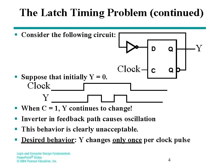
The Latch Timing Problem (continued) § Consider the following circuit: § Suppose that initially Y = 0. Clock D Q Clock Y § § When C = 1, Y continues to change! Inverter in feedback path causes oscillation This behavior is clearly unacceptable. Desired behavior: Y changes only once per clock pulse 4 Y

The Latch Timing Problem (continued) § A solution to the latch timing problem is to break the feedback path § The commonly-used, path-breaking solutions replace the clocked D-latch with: • a master-slave flip-flop • an edge-triggered flip-flop 5

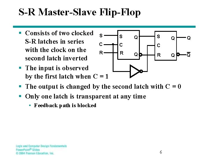
S-R Master-Slave Flip-Flop § Consists of two clocked S S S Q Q S-R latches in series C C C with the clock on the R R Q second latch inverted § The input is observed by the first latch when C = 1 § The output is changed by the second latch with C = 0 § Only one latch is transparent at any time • Feedback path is blocked 6 Q Q

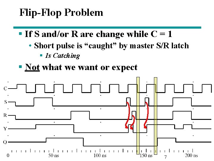
Flip-Flop Problem § If S and/or R are change while C = 1 • Short pulse is “caught” by master S/R latch § 1 s Catching § Not what we want or expect 7

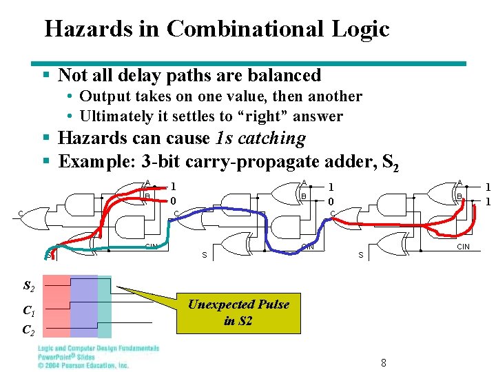
Hazards in Combinational Logic § Not all delay paths are balanced • Output takes on one value, then another • Ultimately it settles to “right” answer § Hazards can cause 1 s catching § Example: 3 -bit carry-propagate adder, S 2 A B C A 1 0 B C S 2 CIN A 1 0 B C S CIN S S 2 C 1 C 2 Unexpected Pulse in S 2 8 1 1

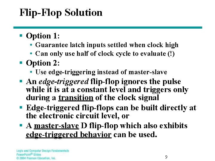
Flip-Flop Solution § Option 1: • Guarantee latch inputs settled when clock high • Can only use half of clock cycle to evaluate (!) § Option 2: • Use edge-triggering instead of master-slave § An edge-triggered flip-flop ignores the pulse while it is at a constant level and triggers only during a transition of the clock signal § Edge-triggered flip-flops can be built directly at the electronic circuit level, or § A master-slave D flip-flop which also exhibits edge-triggered behavior can be used. 9

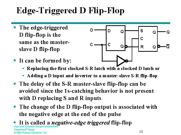
Edge-Triggered D Flip-Flop § The edge-triggered D flip-flop is the same as the masterslave D flip-flop D D Q S Q Q C C C Q R § It can be formed by: • Replacing the first clocked S-R latch with a clocked D latch or • Adding a D input and inverter to a master-slave S-R flip-flop § The delay of the S-R master-slave flip-flop can be avoided since the 1 s-catching behavior is not present with D replacing S and R inputs § The change of the D flip-flop output is associated with the negative edge at the end of the pulse § It is called a negative-edge triggered flip-flop 10

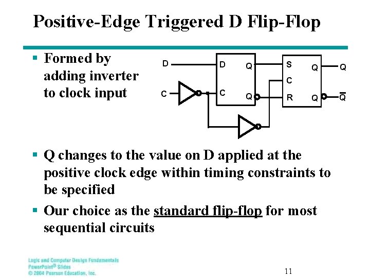
Positive-Edge Triggered D Flip-Flop § Formed by adding inverter to clock input D D Q S Q Q C C C Q R § Q changes to the value on D applied at the positive clock edge within timing constraints to be specified § Our choice as the standard flip-flop for most sequential circuits 11

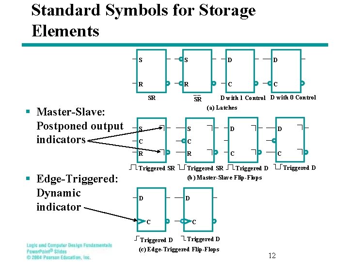
Standard Symbols for Storage Elements S S D D R R C C SR § Master-Slave: Postponed output indicators § Edge-Triggered: Dynamic indicator D with 1 Control D with 0 Control SR (a) Latches S S C C R R Triggered SR Triggered D Triggered SR (b) Master-Slave Flip-Flops D D C C C Triggered D (c) Edge-Triggered Flip-Flops 12 Triggered D

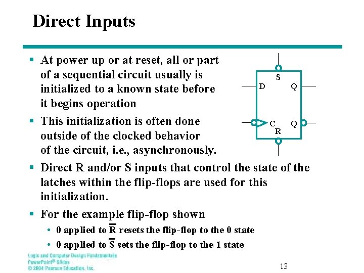
Direct Inputs § At power up or at reset, all or part of a sequential circuit usually is S D Q initialized to a known state before it begins operation § This initialization is often done C Q R outside of the clocked behavior of the circuit, i. e. , asynchronously. § Direct R and/or S inputs that control the state of the latches within the flip-flops are used for this initialization. § For the example flip-flop shown • 0 applied to R resets the flip-flop to the 0 state • 0 applied to S sets the flip-flop to the 1 state 13

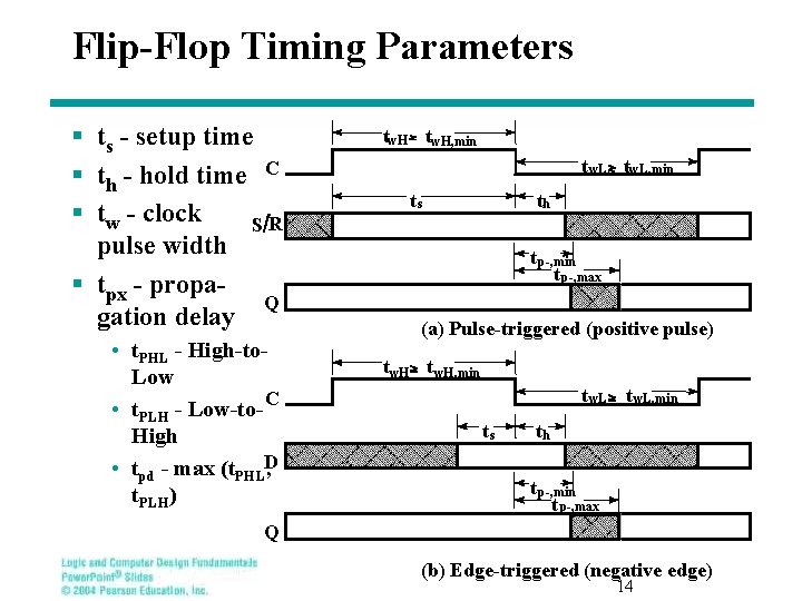
Flip-Flop Timing Parameters § ts - setup time § th - hold time C § tw - clock S/R pulse width § tpx - propa. Q gation delay • t. PHL - High-to. Low C • t. PLH - Low-to. High • tpd - max (t. PHLD , t. PLH) tw. H ≥ tw. H, min tw. L≥ tw. L, min ts th tp-, min t p-, max (a) Pulse-triggered (positive pulse) tw. H≥ t w. H, min tw. L ≥ tw. L, min ts th t p-, min t p-, max Q (b) Edge-triggered (negative edge) 14

Flip-Flop Timing Parameters (continued) § ts - setup time • Master-slave - Equal to the width of the triggering pulse • Edge-triggered - Equal to a time interval that is generally much less than the width of the triggering pulse § th - hold time - Often equal to zero § tpx - propagation delay • Same parameters as for gates except • Measured from clock edge that triggers the output change to the output change 15

Summary § The latch timing problem § Master-slave flip-flop § Edge-triggered flip-flop § Standard symbols for storage elements § Direct inputs to flip-flops § Flip-flop timing 16

Terms of Use § © 2004 by Pearson Education, Inc. All rights reserved. § The following terms of use apply in addition to the standard Pearson Education Legal Notice. § Permission is given to incorporate these materials into classroom presentations and handouts only to instructors adopting Logic and Computer Design Fundamentals as the course text. § Permission is granted to the instructors adopting the book to post these materials on a protected website or protected ftp site in original or modified form. All other website or ftp postings, including those offering the materials for a fee, are prohibited. § You may not remove or in any way alter this Terms of Use notice or any trademark, copyright, or other proprietary notice, including the copyright watermark on each slide. § Return to Title Page 17