ECECS 352 Digital Systems Fundamentals Lecture 27 Memory

- Slides: 30

ECE/CS 352: Digital Systems Fundamentals Lecture 27 – Memory Basics Charles Kime & Thomas Kaminski © 2004 Pearson Education, Inc. Terms of Use (Hyperlinks are active in View Show mode)

Overview § Memory definitions § Random Access Memory (RAM) § Static RAM (SRAM) integrated circuits • Cells and slices • Cell arrays and coincident selection § Arrays of SRAM integrated circuits § Dynamic RAM (DRAM) integrated circuits § DRAM Types • Synchronous (SDRAM) • Double-Data Rate (DDR SRAM) § Arrays of DRAM integrated circuits 2

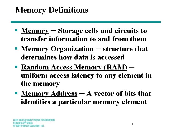
Memory Definitions § Memory ─ Storage cells and circuits to transfer information to and from them § Memory Organization ─ structure that determines how data is accessed § Random Access Memory (RAM) ─ uniform access latency to any element in the memory § Memory Address ─ A vector of bits that identifies a particular memory element 3

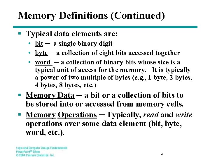
Memory Definitions (Continued) § Typical data elements are: • bit ─ a single binary digit • byte ─ a collection of eight bits accessed together • word ─ a collection of binary bits whose size is a typical unit of access for the memory. It is typically a power of two multiple of bytes (e. g. , 1 byte, 2 bytes, 4 bytes, 8 bytes, etc. ) § Memory Data ─ a bit or a collection of bits to be stored into or accessed from memory cells. § Memory Operations ─ Typically, read and write operations over some data element (bit, byte, word, etc. ). 4

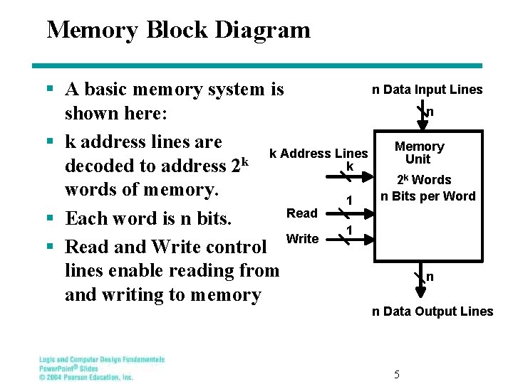
Memory Block Diagram n Data Input Lines § A basic memory system is n shown here: § k address lines are Memory k Address Lines Unit k decoded to address 2 k 2 k Words words of memory. n Bits per Word 1 Read § Each word is n bits. 1 Write § Read and Write control lines enable reading from n and writing to memory n Data Output Lines 5

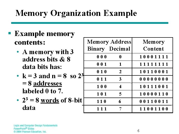
Memory Organization Example § Example memory contents: • A memory with 3 address bits & 8 data bits has: • k = 3 and n = 8 so 23 = 8 addresses labeled 0 to 7. • 23 = 8 words of 8 -bit data Memory Address Binary Decimal Memory Content 0 0 0 1 1 0 2 0 1 1 3 1 0 0 4 1 0 1 5 1 1 0 6 1 0 0 0 1 1 1 1 0 1 1 0 0 0 1 0 0 0 0 1 0 1 1 1 0 0 1 1 0 0 0 1 1 1 1 1 7 1 1 0 0 6

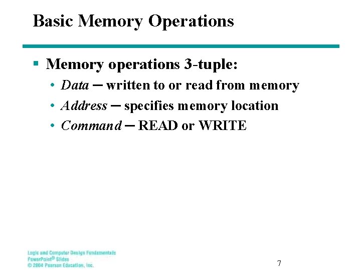
Basic Memory Operations § Memory operations 3 -tuple: • Data ─ written to or read from memory • Address ─ specifies memory location • Command ─ READ or WRITE 7

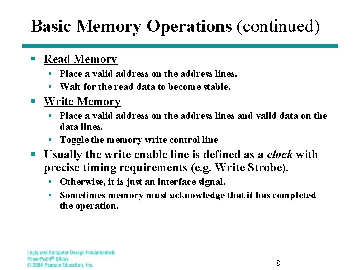
Basic Memory Operations (continued) § Read Memory • Place a valid address on the address lines. • Wait for the read data to become stable. § Write Memory • Place a valid address on the address lines and valid data on the data lines. • Toggle the memory write control line § Usually the write enable line is defined as a clock with precise timing requirements (e. g. Write Strobe). • Otherwise, it is just an interface signal. • Sometimes memory must acknowledge that it has completed the operation. 8

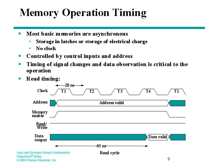
Memory Operation Timing § Most basic memories are asynchronous • Storage in latches or storage of electrical charge • No clock § Controlled by control inputs and address § Timing of signal changes and data observation is critical to the operation § Read timing: Clock Address 20 ns T 1 T 2 T 3 T 4 T 1 Address valid Memory enable Read/ Write Data output Data valid 65 ns Read cycle 9

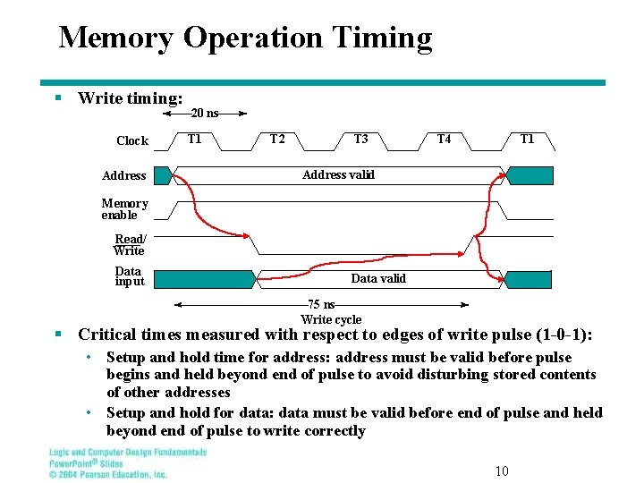
Memory Operation Timing § Write timing: Clock Address 20 ns T 1 T 2 T 3 T 4 T 1 Address valid Memory enable Read/ Write Data input Data valid 75 ns Write cycle § Critical times measured with respect to edges of write pulse (1 -0 -1): • Setup and hold time for address: address must be valid before pulse begins and held beyond end of pulse to avoid disturbing stored contents of other addresses • Setup and hold for data: data must be valid before end of pulse and held beyond end of pulse to write correctly 10

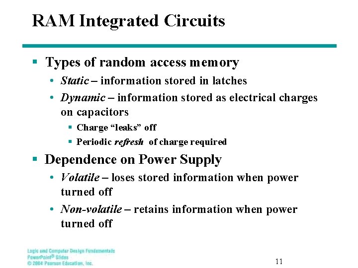
RAM Integrated Circuits § Types of random access memory • Static – information stored in latches • Dynamic – information stored as electrical charges on capacitors § Charge “leaks” off § Periodic refresh of charge required § Dependence on Power Supply • Volatile – loses stored information when power turned off • Non-volatile – retains information when power turned off 11

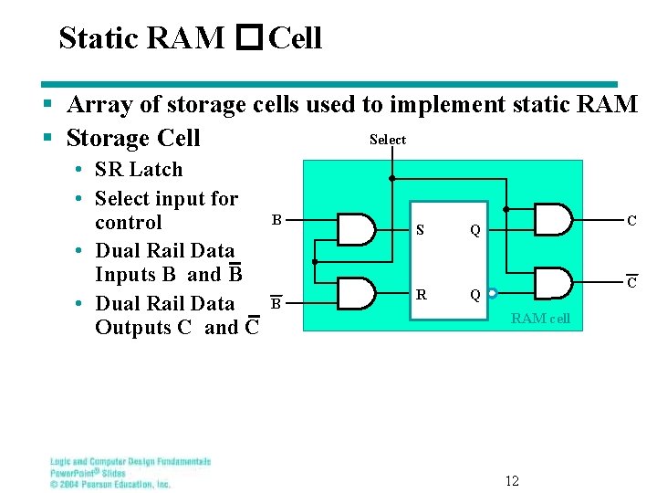
Static RAM � Cell § Array of storage cells used to implement static RAM Select § Storage Cell • SR Latch • Select input for control • Dual Rail Data Inputs B and B • Dual Rail Data Outputs C and C B B S Q R Q C C RAM cell 12

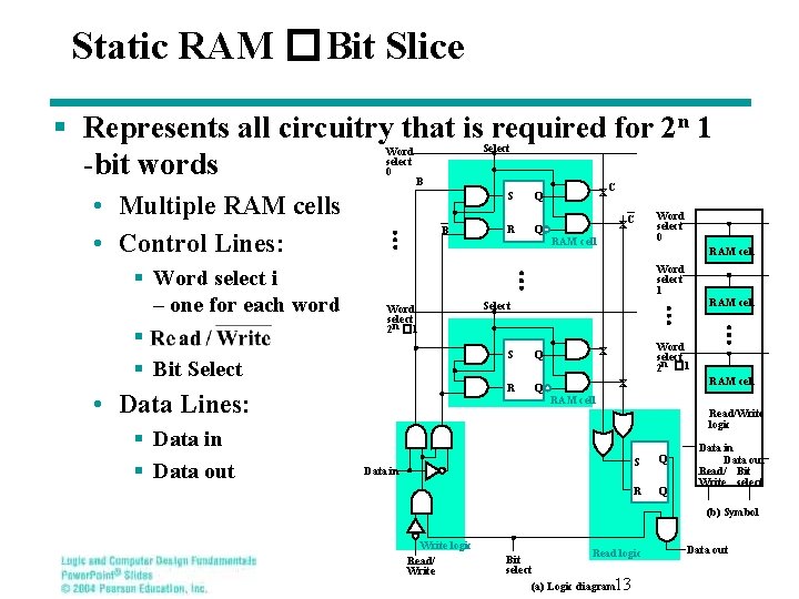
Static RAM � Bit Slice § Represents all circuitry that is required for 2 n 1 -bit words Word select 0 Select B • Multiple RAM cells • Control Lines: § Word select i – one for each word § § Bit Select B Q R Q XC C X RAM cell Word select 0 RAM cell Word select 1 Word select 2 n � 1 • Data Lines: § Data in § Data out S RAM cell Select S Q R Q Word select 2 n � 1 X RAM cell Read/Write logic Data in S Q R Q Data in Data out Read/ Bit Write select (b) Symbol Write logic Read/ Write Read logic Bit select (a) Logic diagram 13 Data out

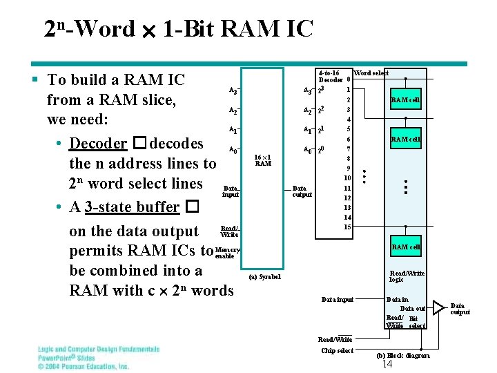
2 n-Word 1 -Bit RAM IC § To build a RAM IC A 3 from a RAM slice, A 2 we need: A 1 • Decoder � decodes A 0 the n address lines to 2 n word select lines Data input • A 3 -state buffer � on the data output Read/ Write permits RAM ICs to Memory enable be combined into a RAM with c 2 n words A 3 A 2 A 1 16 x 1 RAM A 0 Data output Word select 4 -to-16 Decoder 0 1 23 2 RAM cell 3 22 4 5 21 6 RAM cell 0 7 2 8 9 10 11 12 13 14 15 RAM cell Read/Write logic (a) Symbol Data input Data in Data out Read/ Bit Write select Read/Write Chip select (b) Block diagram 14 Data output

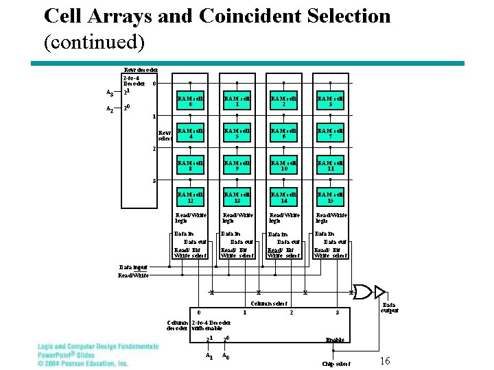
Cell Arrays and Coincident Selection § Memory arrays can be very large => • Large decoders • Large fanouts for the bit lines • The decoder size and fanouts can be reduced by approximately by using a coincident selection in a 2 -dimensional array • Uses two decoders, one for words and one for bits • Word select becomes Row select • Bit select becomes Column select § See next slide for example • A 3 and A 2 used for Row select • A 1 and A 0 for Column select 15

Cell Arrays and Coincident Selection (continued) A 3 Row decoder 2 -to-4 Decoder 0 21 A 2 20 RAM cell 1 RAM cell 2 RAM cell 3 Row RAM cell 4 select RAM cell 5 RAM cell 6 RAM cell 7 RAM cell 8 RAM cell 9 RAM cell 10 RAM cell 11 RAM cell 12 RAM cell 13 RAM cell 14 RAM cell 15 Read/Write logic Data in Data out Read/ Bit Write select 1 2 3 Data input Read/Write X X Column select 0 1 Column 2 -to-4 Decoder decoder with enable 21 20 A 1 A 0 2 3 Data output Enable Chip select 16

RAM ICs with > 1 Bit/Word § Word length can be quite high. § To better balance the number of words and word length, use ICs with > 1 bit/word 17

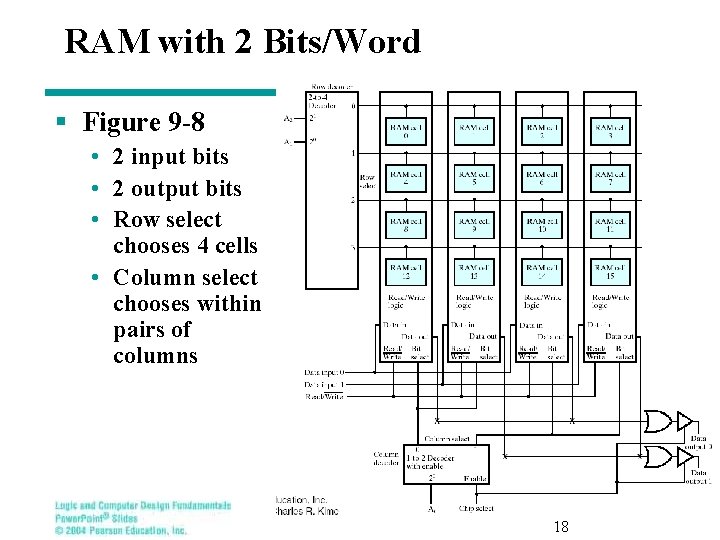
RAM with 2 Bits/Word § Figure 9 -8 • 2 input bits • 2 output bits • Row select chooses 4 cells • Column select chooses within pairs of columns 18

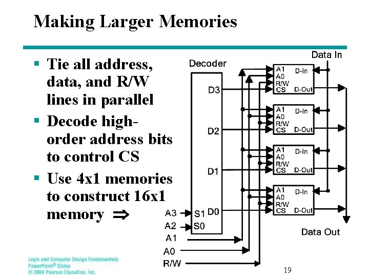
Making Larger Memories § Tie all address, data, and R/W lines in parallel § Decode highorder address bits to control CS § Use 4 x 1 memories to construct 16 x 1 memory 19

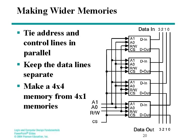
Making Wider Memories § Tie address and control lines in parallel § Keep the data lines separate § Make a 4 x 4 memory from 4 x 1 memories 20

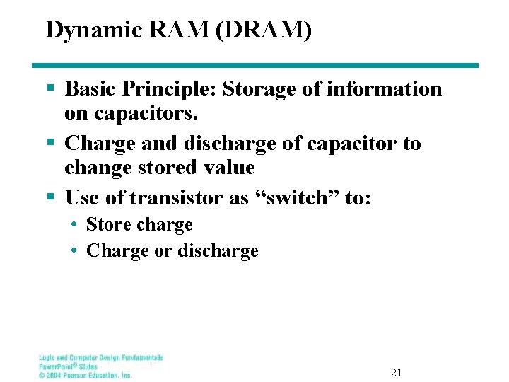
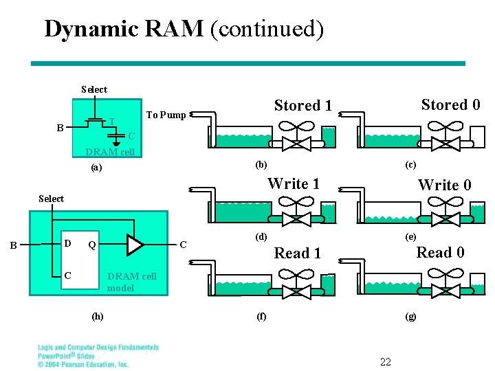
Dynamic RAM (DRAM) § Basic Principle: Storage of information on capacitors. § Charge and discharge of capacitor to change stored value § Use of transistor as “switch” to: • Store charge • Charge or discharge 21

Dynamic RAM (continued) Select T B Stored 0 Stored 1 To Pump C DRAM cell (b) (a) (c) Write 1 Write 0 Select B D Q C C (d) (e) Read 0 Read 1 DRAM cell model (h) (f) (g) 22

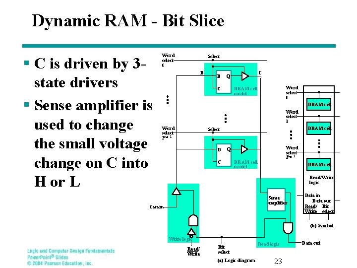
Dynamic RAM - Bit Slice § C is driven by 3 state drivers § Sense amplifier is used to change the small voltage change on C into H or L Word select 0 Select B D C Q C Word select 0 DRAM cell model DRAM cell Word select 1 Word select 2 n 2 1 DRAM cell Select D Word select 2 n 2 1 Q C DRAM cell model DRAM cell Read/Write logic Sense amplifier Data in Data out Read/ Bit Write select (b) Symbol Write logic Read/ Write Bit select (a) Logic diagram Read logic 23 Data out

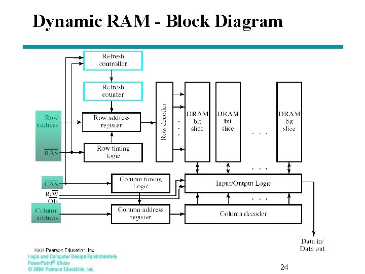
Dynamic RAM - Block Diagram 24

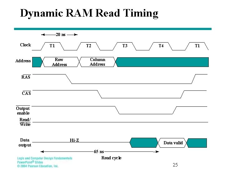
Dynamic RAM Read Timing 20 ns Clock Address T 1 T 2 T 3 T 4 T 1 Column Address Row Address RAS CAS Output enable Read/ Write Data output Hi-Z Data valid 65 ns Read cycle 25

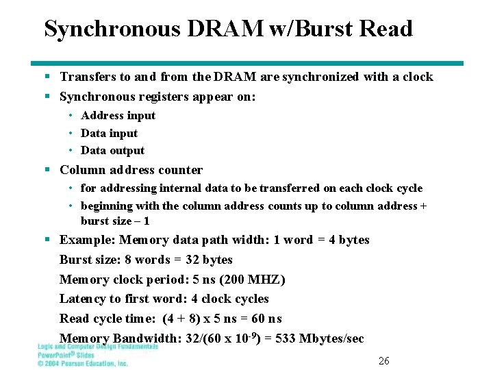
Synchronous DRAM w/Burst Read § Transfers to and from the DRAM are synchronized with a clock § Synchronous registers appear on: • Address input • Data output § Column address counter • for addressing internal data to be transferred on each clock cycle • beginning with the column address counts up to column address + burst size – 1 § Example: Memory data path width: 1 word = 4 bytes Burst size: 8 words = 32 bytes Memory clock period: 5 ns (200 MHZ) Latency to first word: 4 clock cycles Read cycle time: (4 + 8) x 5 ns = 60 ns Memory Bandwidth: 32/(60 x 10 -9) = 533 Mbytes/sec 26

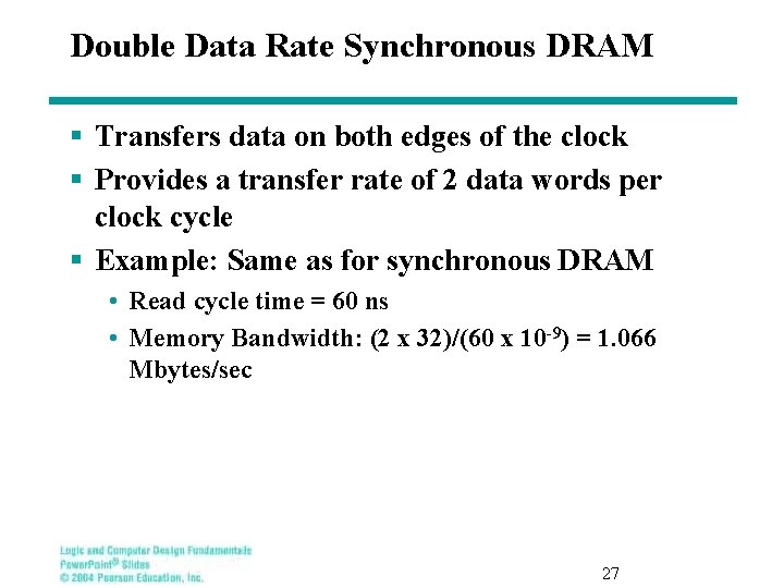
Double Data Rate Synchronous DRAM § Transfers data on both edges of the clock § Provides a transfer rate of 2 data words per clock cycle § Example: Same as for synchronous DRAM • Read cycle time = 60 ns • Memory Bandwidth: (2 x 32)/(60 x 10 -9) = 1. 066 Mbytes/sec 27

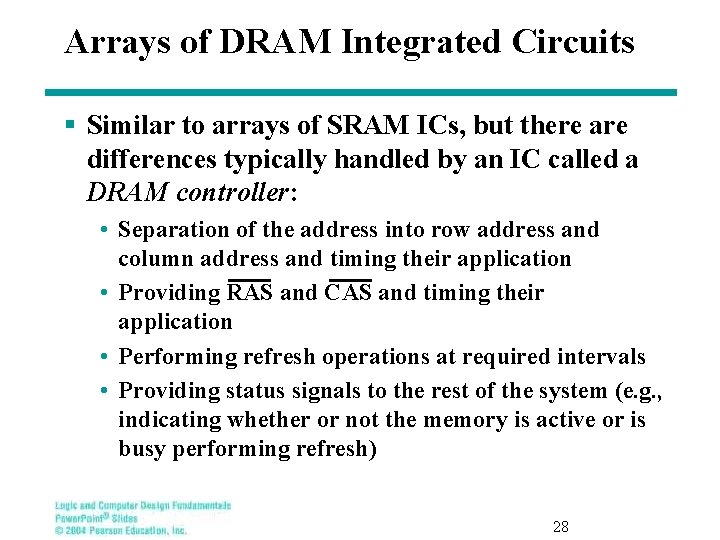
Arrays of DRAM Integrated Circuits § Similar to arrays of SRAM ICs, but there are differences typically handled by an IC called a DRAM controller: • Separation of the address into row address and column address and timing their application • Providing RAS and CAS and timing their application • Performing refresh operations at required intervals • Providing status signals to the rest of the system (e. g. , indicating whether or not the memory is active or is busy performing refresh) 28

Summary § Memory definitions § Random Access Memory (RAM) § Static RAM (SRAM) integrated circuits • Cells and slices • Cell arrays and coincident selection § Arrays of SRAM integrated circuits § Dynamic RAM (DRAM) integrated circuits § DRAM Types • Synchronous (SDRAM) • Double-Data Rate (DDR SRAM) § Arrays of DRAM integrated circuits 29

Terms of Use § © 2004 by Pearson Education, Inc. All rights reserved. § The following terms of use apply in addition to the standard Pearson Education Legal Notice. § Permission is given to incorporate these materials into classroom presentations and handouts only to instructors adopting Logic and Computer Design Fundamentals as the course text. § Permission is granted to the instructors adopting the book to post these materials on a protected website or protected ftp site in original or modified form. All other website or ftp postings, including those offering the materials for a fee, are prohibited. § You may not remove or in any way alter this Terms of Use notice or any trademark, copyright, or other proprietary notice, including the copyright watermark on each slide. § Return to Title Page 30