ECECS 352 Digital Systems Fundamentals Lecture 20 Analyzing

- Slides: 23

ECE/CS 352: Digital Systems Fundamentals Lecture 20 – Analyzing Sequential Logic Charles Kime & Thomas Kaminski © 2004 Pearson Education, Inc. Terms of Use (Hyperlinks are active in View Show mode)

Overview § Finite State Machine Model § State Tables § State Diagrams § Moore and Mealy Models § Circuit and System Level Timing 2

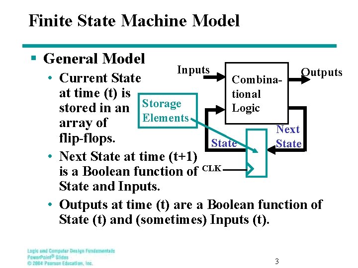
Finite State Machine Model § General Model Inputs Outputs • Current State Combinaat time (t) is tional Storage Logic stored in an Elements array of Next flip-flops. State • Next State at time (t+1) CLK is a Boolean function of State and Inputs. • Outputs at time (t) are a Boolean function of State (t) and (sometimes) Inputs (t). 3

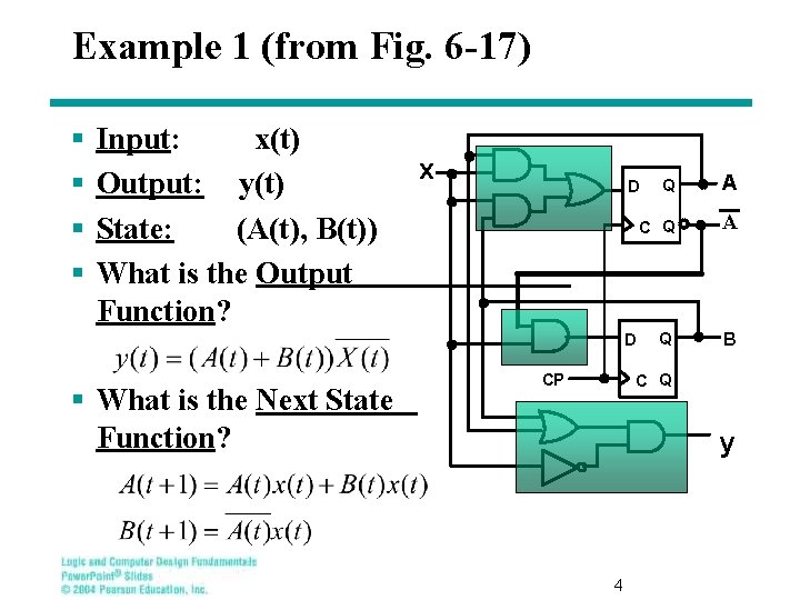
Example 1 (from Fig. 6 -17) § § Input: x(t) x Output: y(t) State: (A(t), B(t)) What is the Output Function? D § What is the Next State Function? Q A C Q A Q B D CP C Q y 4

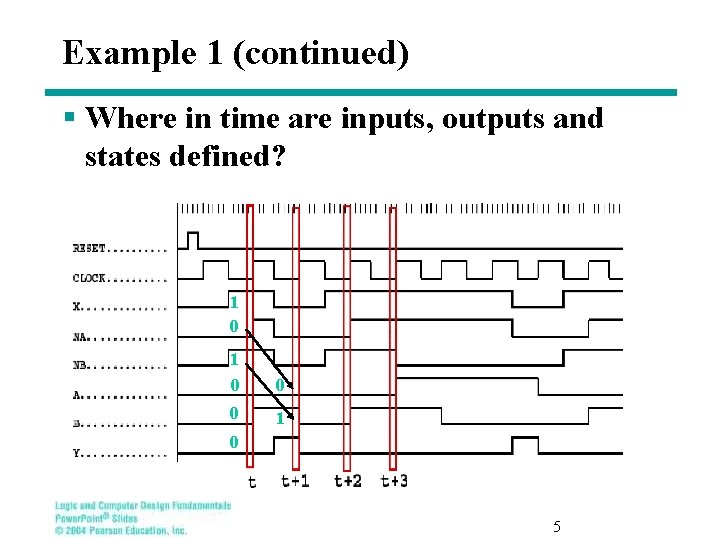
Example 1 (continued) § Where in time are inputs, outputs and states defined? 1 0 0 0 1 0 5

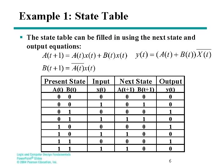
Example 1: State Table § The state table can be filled in using the next state and output equations: Present State Input A(t) B(t) 0 0 0 1 0 1 1 1 1 x(t) 0 1 0 1 Next State Output A(t+1) B(t+1) 0 0 0 1 0 0 1 0 y(t) 0 0 1 0 1 0 6

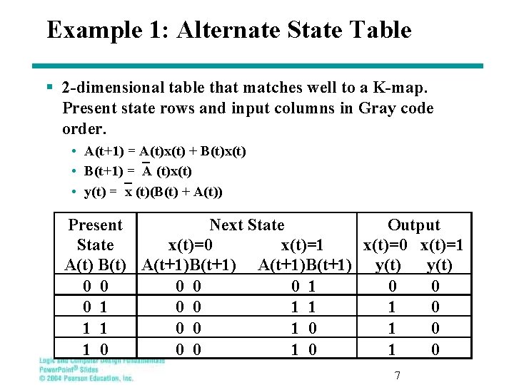
Example 1: Alternate State Table § 2 -dimensional table that matches well to a K-map. Present state rows and input columns in Gray code order. • A(t+1) = A(t)x(t) + B(t)x(t) • B(t+1) = A (t)x(t) • y(t) = x (t)(B(t) + A(t)) Present Next State Output State x(t)=0 x(t)=1 x(t)=0 x(t)=1 A(t) B(t) A(t+1)B(t+1) y(t) 0 0 0 1 0 0 0 1 0 0 1 1 1 0 1 1 0 0 1 0 1 0 0 0 1 0 1 0 7

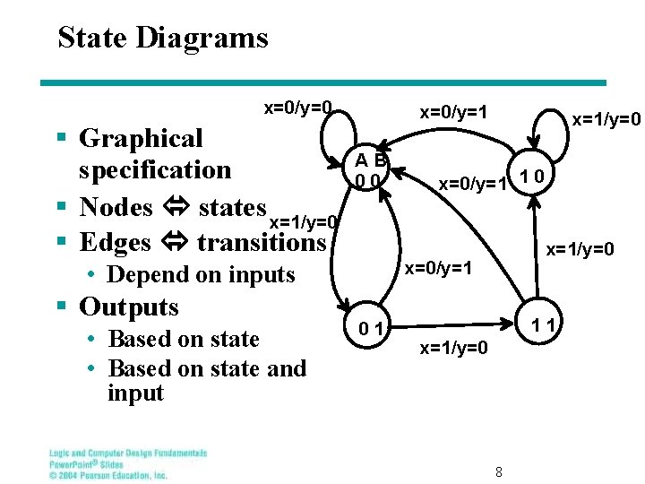
State Diagrams x=0/y=0 § Graphical specification § Nodes states x=1/y=0 § Edges transitions x=0/y=1 AB 00 • Based on state and input x=0/y=1 1 0 x=1/y=0 x=0/y=1 • Depend on inputs § Outputs x=1/y=0 01 11 x=1/y=0 8

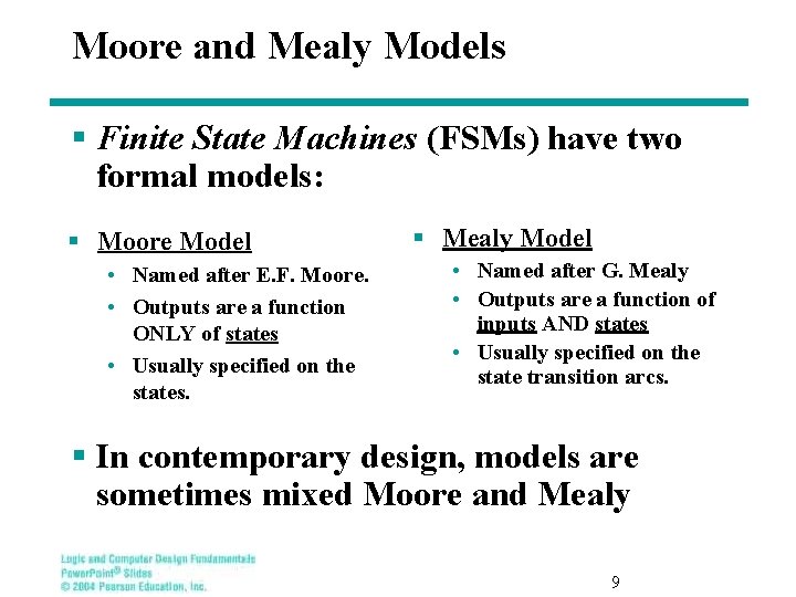
Moore and Mealy Models § Finite State Machines (FSMs) have two formal models: § Moore Model • Named after E. F. Moore. • Outputs are a function ONLY of states • Usually specified on the states. § Mealy Model • Named after G. Mealy • Outputs are a function of inputs AND states • Usually specified on the state transition arcs. § In contemporary design, models are sometimes mixed Moore and Mealy 9

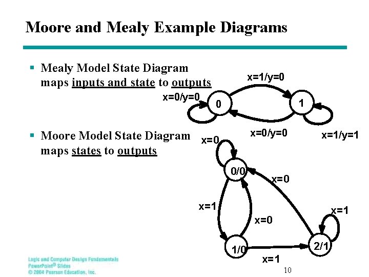
Moore and Mealy Example Diagrams § Mealy Model State Diagram maps inputs and state to outputs x=0/y=0 x=1/y=0 1 0 x=0/y=0 x=1/y=1 § Moore Model State Diagram x=0 maps states to outputs 0/0 x=1 x=0 1/0 2/1 x=1 10

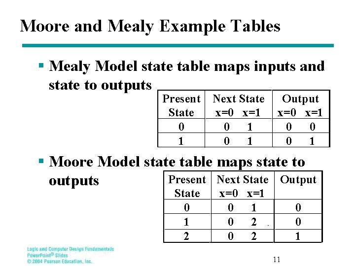
Moore and Mealy Example Tables § Mealy Model state table maps inputs and state to outputs Present Next State Output State x=0 x=1 0 0 1 0 1 § Moore Model state table maps state to Present Next State Output outputs State 0 1 2 x=0 x=1 0 2 0 2 0 0 1 11

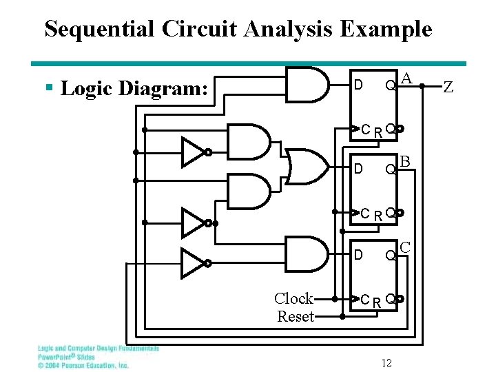
Sequential Circuit Analysis Example § Logic Diagram: D Q A C RQ D Q B C RQ D Clock Reset Q CR Q 12 C Z

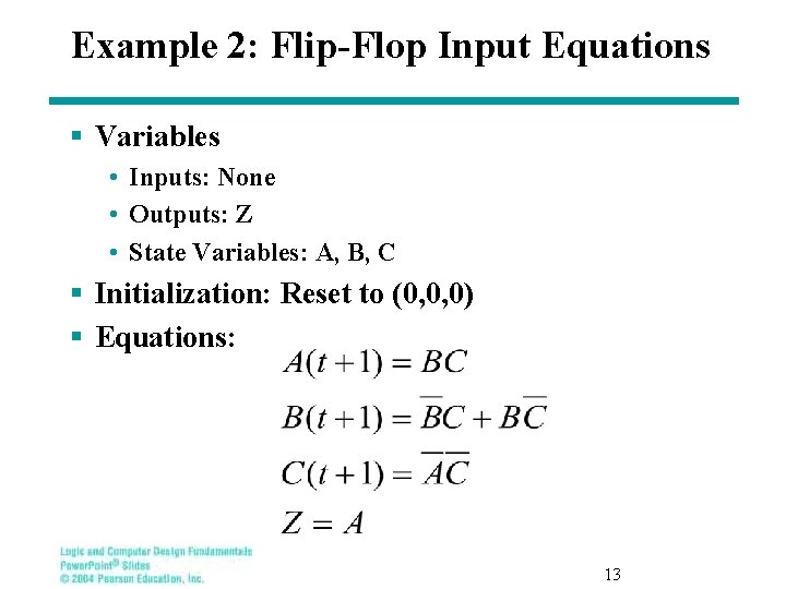
Example 2: Flip-Flop Input Equations § Variables • Inputs: None • Outputs: Z • State Variables: A, B, C § Initialization: Reset to (0, 0, 0) § Equations: 13

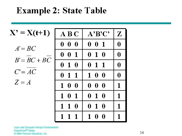
Example 2: State Table X’ = X(t+1) A B C A’B’C’ Z 0 0 0 1 0 0 1 1 1 0 0 1 0 1 1 1 0 1 1 1 0 0 1 0 0 1 1 1 0 0 0 1 0 0 1 1 14

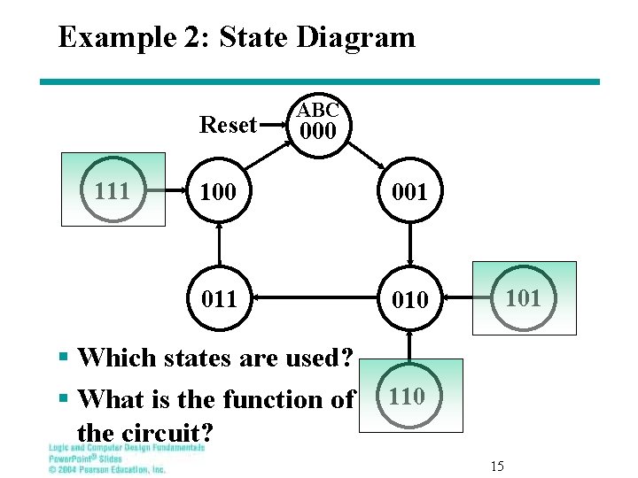
Example 2: State Diagram Reset 111 ABC 000 100 001 010 § Which states are used? § What is the function of the circuit? 101 110 15

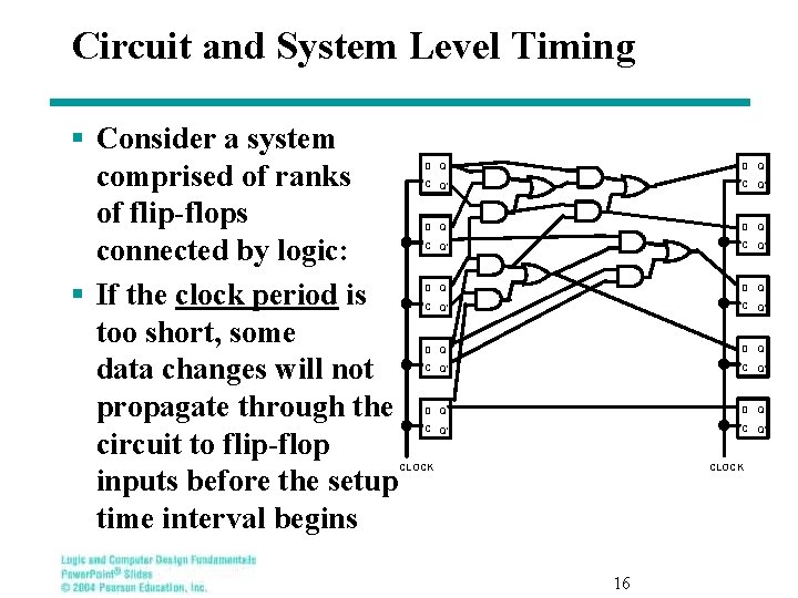
Circuit and System Level Timing § Consider a system comprised of ranks of flip-flops connected by logic: § If the clock period is too short, some data changes will not propagate through the circuit to flip-flop inputs before the setup time interval begins D Q D Q C Q' C Q' D Q C Q' CLOCK 16

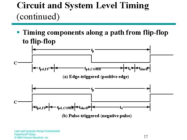
Circuit and System Level Timing (continued) § Timing components along a path from flip-flop to flip-flop tp C tpd, FF tpd, COMB ts tslack (a) Edge-triggered (positive edge) tp C tpd, FF tpd, COMB tslack ts (b) Pulse-triggered (negative pulse) 17

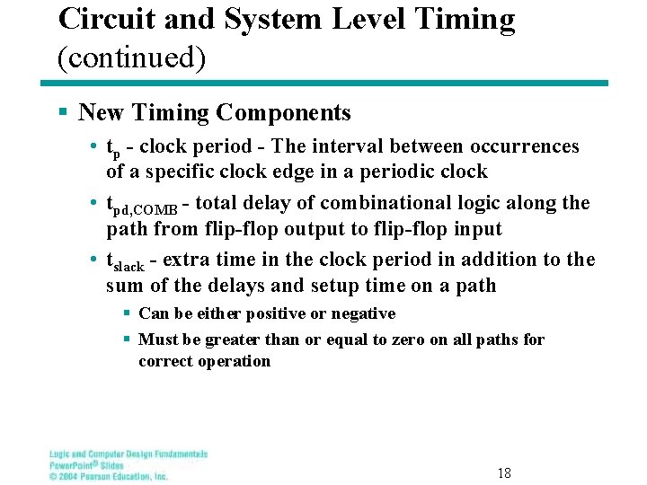
Circuit and System Level Timing (continued) § New Timing Components • tp - clock period - The interval between occurrences of a specific clock edge in a periodic clock • tpd, COMB - total delay of combinational logic along the path from flip-flop output to flip-flop input • tslack - extra time in the clock period in addition to the sum of the delays and setup time on a path § Can be either positive or negative § Must be greater than or equal to zero on all paths for correct operation 18

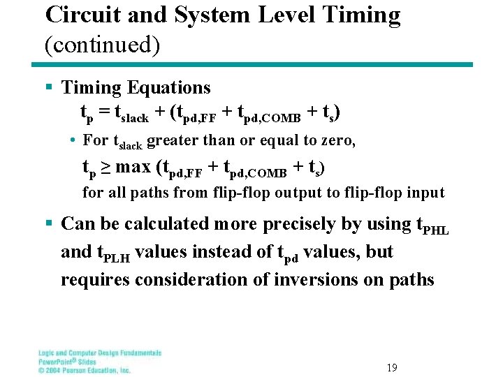
Circuit and System Level Timing (continued) § Timing Equations tp = tslack + (tpd, FF + tpd, COMB + ts) • For tslack greater than or equal to zero, tp ≥ max (tpd, FF + tpd, COMB + ts) for all paths from flip-flop output to flip-flop input § Can be calculated more precisely by using t. PHL and t. PLH values instead of tpd values, but requires consideration of inversions on paths 19

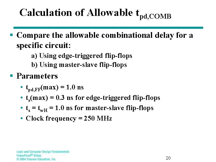
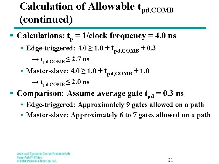
Calculation of Allowable tpd, COMB § Compare the allowable combinational delay for a specific circuit: a) Using edge-triggered flip-flops b) Using master-slave flip-flops § Parameters • • tpd, FF(max) = 1. 0 ns ts(max) = 0. 3 ns for edge-triggered flip-flops ts = tw. H = 1. 0 ns for master-slave flip-flops Clock frequency = 250 MHz 20

Calculation of Allowable tpd, COMB (continued) § Calculations: tp = 1/clock frequency = 4. 0 ns • Edge-triggered: 4. 0 ≥ 1. 0 + tpd, COMB + 0. 3 → tpd, COMB ≤ 2. 7 ns • Master-slave: 4. 0 ≥ 1. 0 + tpd, COMB + 1. 0 → tpd, COMB ≤ 2. 0 ns § Comparison: Assume average gate tpd = 0. 3 ns • Edge-triggered: Approximately 9 gates allowed on a path • Master-slave: Approximately 6 to 7 gates allowed on a path 21

Summary § Finite State Machine Model § State Tables § State Diagrams § Moore and Mealy Models § Circuit and System Level Timing 22

Terms of Use § © 2004 by Pearson Education, Inc. All rights reserved. § The following terms of use apply in addition to the standard Pearson Education Legal Notice. § Permission is given to incorporate these materials into classroom presentations and handouts only to instructors adopting Logic and Computer Design Fundamentals as the course text. § Permission is granted to the instructors adopting the book to post these materials on a protected website or protected ftp site in original or modified form. All other website or ftp postings, including those offering the materials for a fee, are prohibited. § You may not remove or in any way alter this Terms of Use notice or any trademark, copyright, or other proprietary notice, including the copyright watermark on each slide. § Return to Title Page 23