ECE 252 CPS 220 Advanced Computer Architecture I

![Packaging & 3 D Stacking [ Apple A 4 package on circuit board ] Packaging & 3 D Stacking [ Apple A 4 package on circuit board ]](https://slidetodoc.com/presentation_image/79fb71e4c5599d117885a31ce4751316/image-9.jpg)

- Slides: 32

ECE 252 / CPS 220 Advanced Computer Architecture I Lecture 12 Memory – Part 1 Benjamin Lee Electrical and Computer Engineering Duke University www. duke. edu/~bcl 15/class_ece 252 fall 11. html

ECE 252 Administrivia 20 October – Homework #3 Due 20 October – Project Proposals Due One page proposal 1. What question are you asking? 2. How are you going to answer that question? 3. Talk to me if you are looking for project ideas. 25 October – Class Discussion 1. 2. 3. 4. Roughly one reading per class. Do not wait until the day before! Jouppi. “Improving direct-mapped cache performance by the addition of a small fully-associative cache and prefetch buffers. ” Kim et al. “An adaptive, non-uniform cache structure for wire-delay dominated on-chip caches. ” Fromm et al. “The energy efficiency of IRAM architectures” Lee et al. “Phase change memory architecture and the quest for scalability” ECE 252 / CPS 220 2

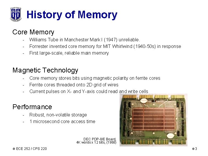
History of Memory Core Memory - Williams Tube in Manchester Mark I (1947) unreliable. Forrester invented core memory for MIT Whirlwind (1940 -50 s) in response First large-scale, reliable main memory Magnetic Technology - Core memory stores bits using magnetic polarity on ferrite cores Ferrite cores threaded onto 2 D grid of wires Current pulses on X- and Y-axis could read and write cells Performance - Robust, non-volatile storage 1 microsecond core access time DEC PDP-8/E Board, 4 K words x 12 bits, (1968) ECE 252 / CPS 220 3

Semiconductor Memory - Static RAM (SRAM): cross-coupled inverters latch value Dynamic RAM (DRAM): charge stored on a capacitor Advent of Semiconductor Memory - Technology became competitive in early 1970 s Intel founded to exploit market for semiconductor memory Dynamic Random Access Memory (DRAM) - Charge on a capacitor maps to logical value Intel 1103 was first commercial DRAM Semiconductor memory quickly replaced core memory in 1970’s ECE 252 / CPS 220 4

Semiconductor Memory Advent of Semiconductor Memory - Technology became competitive in early 1970 s Intel founded to exploit market for semiconductor memory Early semiconductor memory was static RAM (SRAM). SRAM cell internals similar to a latch (cross-coupled inverters) - Advent of Semiconductor Memory 25 October – Class Discussion 1. 2. 3. 4. Roughly one reading per class. Do not wait until the day before! Jouppi. “Improving direct-mapped cache performance by the addition of a small fully-associative cache and prefetch buffers. ” Kim et al. “An adaptive, non-uniform cache structure for wire-delay dominated on-chip caches. ” Fromm et al. “The energy efficiency of IRAM architectures” Lee et al. “Phase change memory architecture and the quest for scalability” ECE 252 / CPS 220 5

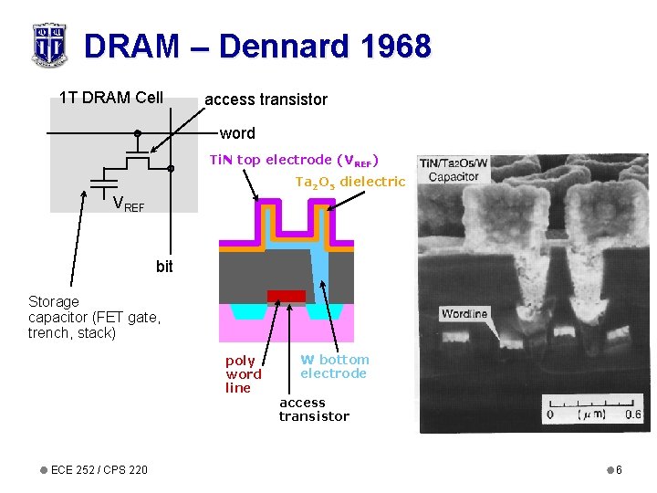
DRAM – Dennard 1968 1 T DRAM Cell access transistor word Ti. N top electrode (VREF) Ta 2 O 5 dielectric VREF bit Storage capacitor (FET gate, trench, stack) poly word line ECE 252 / CPS 220 W bottom electrode access transistor 6

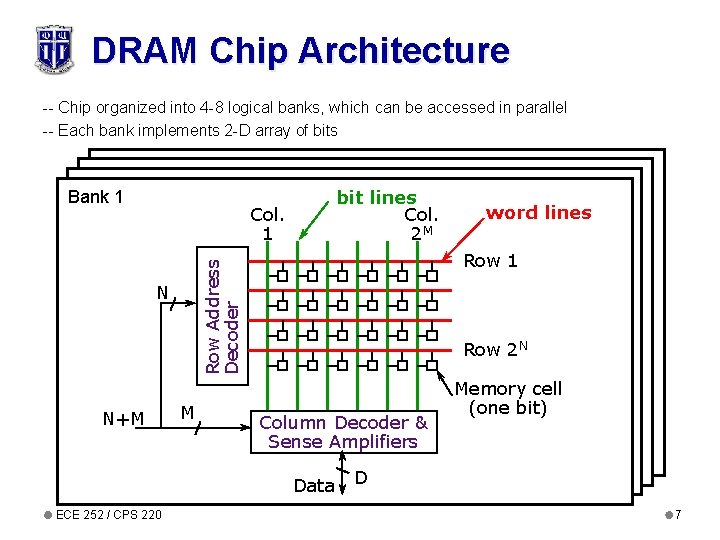
DRAM Chip Architecture -- Chip organized into 4 -8 logical banks, which can be accessed in parallel -- Each bank implements 2 -D array of bits Bank 1 bit lines Col. 2 M Col. 1 N+M Row 1 Row Address Decoder N M Row 2 N Column Decoder & Sense Amplifiers Data ECE 252 / CPS 220 word lines Memory cell (one bit) D 7

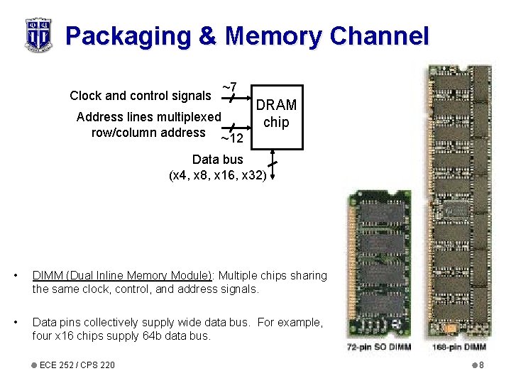
Packaging & Memory Channel Clock and control signals ~7 Address lines multiplexed row/column address ~12 DRAM chip Data bus (x 4, x 8, x 16, x 32) • DIMM (Dual Inline Memory Module): Multiple chips sharing the same clock, control, and address signals. • Data pins collectively supply wide data bus. For example, four x 16 chips supply 64 b data bus. ECE 252 / CPS 220 8
![Packaging 3 D Stacking Apple A 4 package on circuit board Packaging & 3 D Stacking [ Apple A 4 package on circuit board ]](https://slidetodoc.com/presentation_image/79fb71e4c5599d117885a31ce4751316/image-9.jpg)
Packaging & 3 D Stacking [ Apple A 4 package on circuit board ] Two stacked DRAM die Processor plus logic die [ Apple A 4 package cross-section, i. Fixit 2010 ] ECE 252 / CPS 220 9

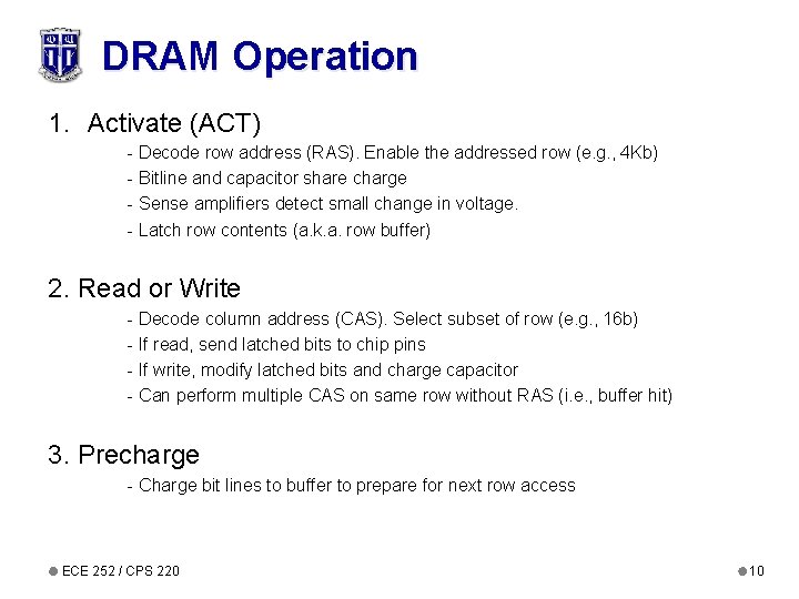
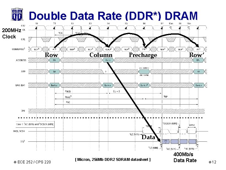
DRAM Operation 1. Activate (ACT) - Decode row address (RAS). Enable the addressed row (e. g. , 4 Kb) - Bitline and capacitor share charge - Sense amplifiers detect small change in voltage. - Latch row contents (a. k. a. row buffer) 2. Read or Write - Decode column address (CAS). Select subset of row (e. g. , 16 b) - If read, send latched bits to chip pins - If write, modify latched bits and charge capacitor - Can perform multiple CAS on same row without RAS (i. e. , buffer hit) 3. Precharge - Charge bit lines to buffer to prepare for next row access ECE 252 / CPS 220 10

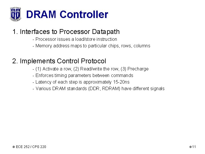
DRAM Controller 1. Interfaces to Processor Datapath - Processor issues a load/store instruction - Memory address maps to particular chips, rows, columns 2. Implements Control Protocol - (1) Activate a row, (2) Read/write the row, (3) Precharge - Enforces timing parameters between commands - Latency of each step is approximately 15 -20 ns - Various DRAM standards (DDR, RDRAM) have different signals ECE 252 / CPS 220 11

Double Data Rate (DDR*) DRAM 200 MHz Clock Row Column Precharge Row’ Data ECE 252 / CPS 220 [ Micron, 256 Mb DDR 2 SDRAM datasheet ] 400 Mb/s Data Rate 12

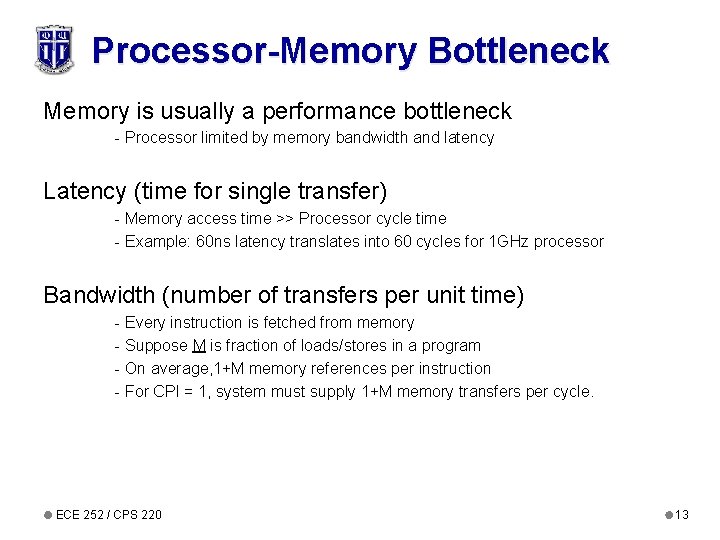
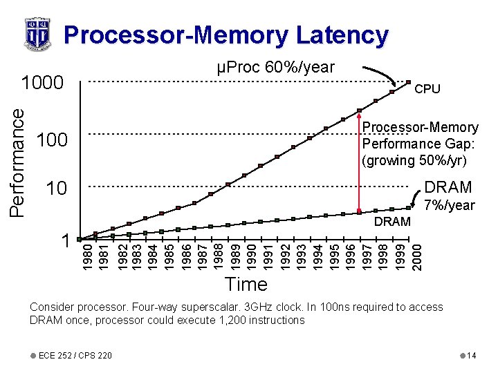
Processor-Memory Bottleneck Memory is usually a performance bottleneck - Processor limited by memory bandwidth and latency Latency (time for single transfer) - Memory access time >> Processor cycle time - Example: 60 ns latency translates into 60 cycles for 1 GHz processor Bandwidth (number of transfers per unit time) - Every instruction is fetched from memory - Suppose M is fraction of loads/stores in a program - On average, 1+M memory references per instruction - For CPI = 1, system must supply 1+M memory transfers per cycle. ECE 252 / CPS 220 13

Processor-Memory Latency µProc 60%/year CPU Processor-Memory Performance Gap: (growing 50%/yr) 100 10 DRAM 7%/year 1 1982 1983 1984 1985 1986 1987 1988 1989 1990 1991 1992 1993 1994 1995 1996 1997 1998 1999 2000 DRAM 1980 1981 Performance 1000 Time Consider processor. Four-way superscalar. 3 GHz clock. In 100 ns required to access DRAM once, processor could execute 1, 200 instructions ECE 252 / CPS 220 14

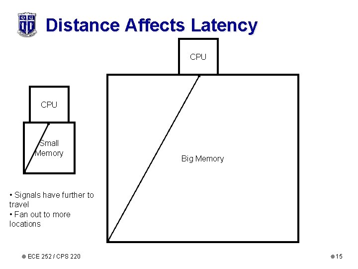
Distance Affects Latency CPU Small Memory Big Memory • Signals have further to travel • Fan out to more locations ECE 252 / CPS 220 15

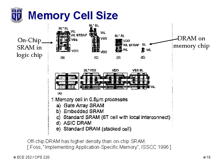
Memory Cell Size On-Chip SRAM in logic chip DRAM on memory chip Off-chip DRAM has higher density than on-chip SRAM. [ Foss, “Implementing Application-Specific Memory”, ISSCC 1996 ] ECE 252 / CPS 220 16

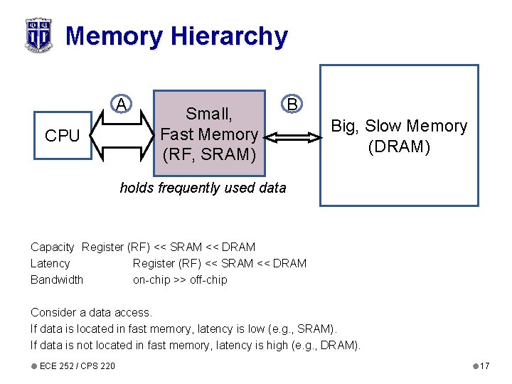
Memory Hierarchy A CPU Small, Fast Memory (RF, SRAM) B Big, Slow Memory (DRAM) holds frequently used data Capacity Register (RF) << SRAM << DRAM Latency Register (RF) << SRAM << DRAM Bandwidth on-chip >> off-chip Consider a data access. If data is located in fast memory, latency is low (e. g. , SRAM). If data is not located in fast memory, latency is high (e. g. , DRAM). ECE 252 / CPS 220 17

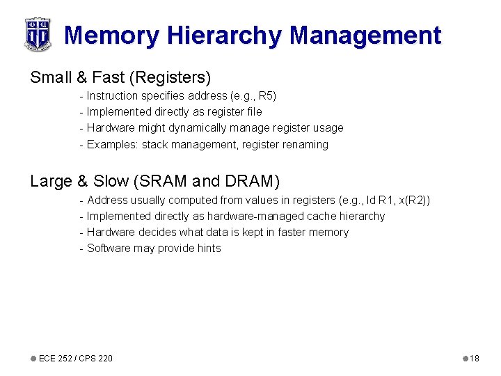
Memory Hierarchy Management Small & Fast (Registers) - Instruction specifies address (e. g. , R 5) - Implemented directly as register file - Hardware might dynamically manage register usage - Examples: stack management, register renaming Large & Slow (SRAM and DRAM) - Address usually computed from values in registers (e. g. , ld R 1, x(R 2)) - Implemented directly as hardware-managed cache hierarchy - Hardware decides what data is kept in faster memory - Software may provide hints ECE 252 / CPS 220 18

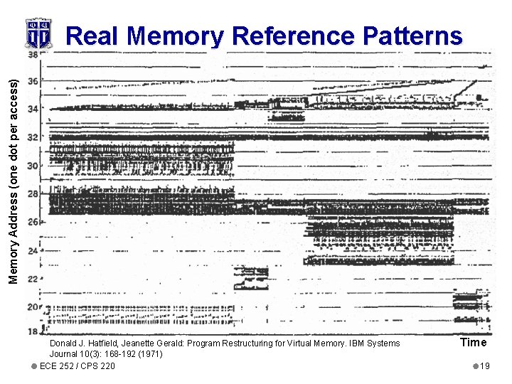
Memory Address (one dot per access) Real Memory Reference Patterns Donald J. Hatfield, Jeanette Gerald: Program Restructuring for Virtual Memory. IBM Systems Journal 10(3): 168 -192 (1971) ECE 252 / CPS 220 Time 19

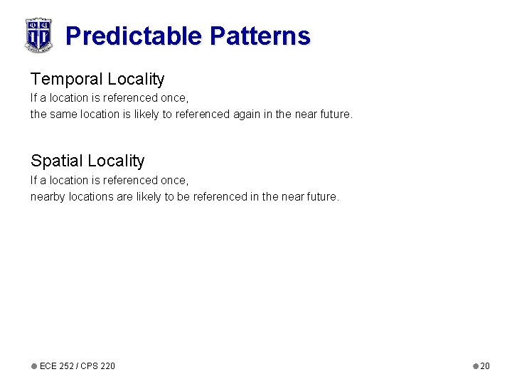
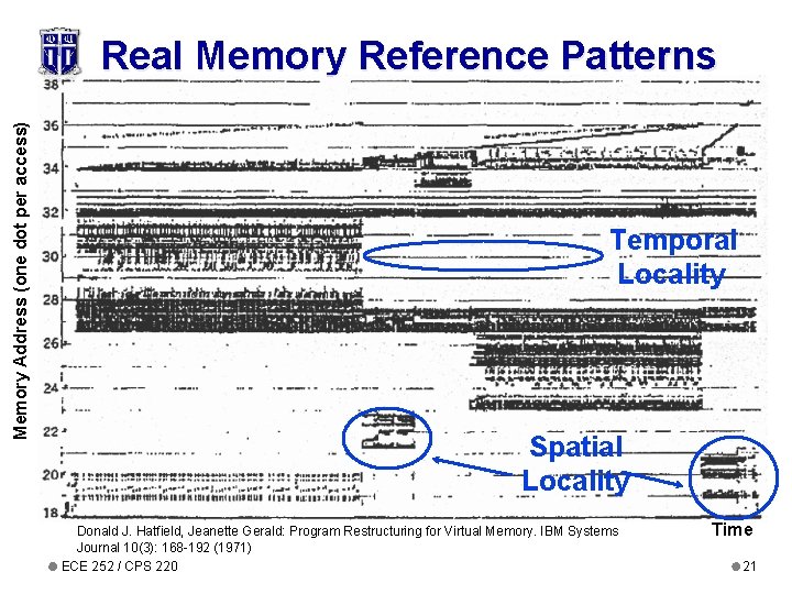
Predictable Patterns Temporal Locality If a location is referenced once, the same location is likely to referenced again in the near future. Spatial Locality If a location is referenced once, nearby locations are likely to be referenced in the near future. ECE 252 / CPS 220 20

Memory Address (one dot per access) Real Memory Reference Patterns Temporal Locality Spatial Locality Donald J. Hatfield, Jeanette Gerald: Program Restructuring for Virtual Memory. IBM Systems Journal 10(3): 168 -192 (1971) ECE 252 / CPS 220 Time 21

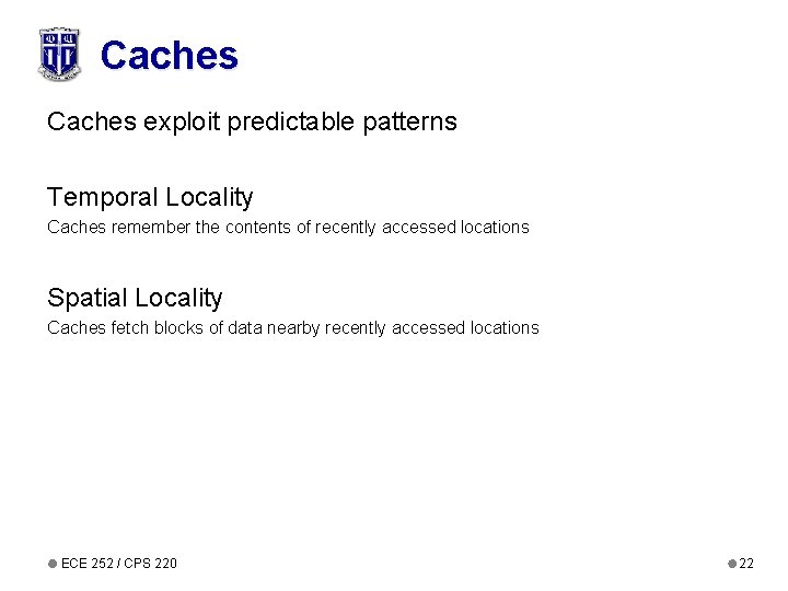
Caches exploit predictable patterns Temporal Locality Caches remember the contents of recently accessed locations Spatial Locality Caches fetch blocks of data nearby recently accessed locations ECE 252 / CPS 220 22

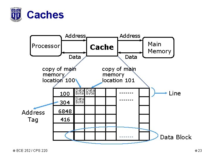
Caches Address Processor Address Cache Data copy of main memory location 100 304 Address Tag Data Byte Data Main Memory copy of main memory location 101 Line Data Byte 6848 416 Data Block ECE 252 / CPS 220 23

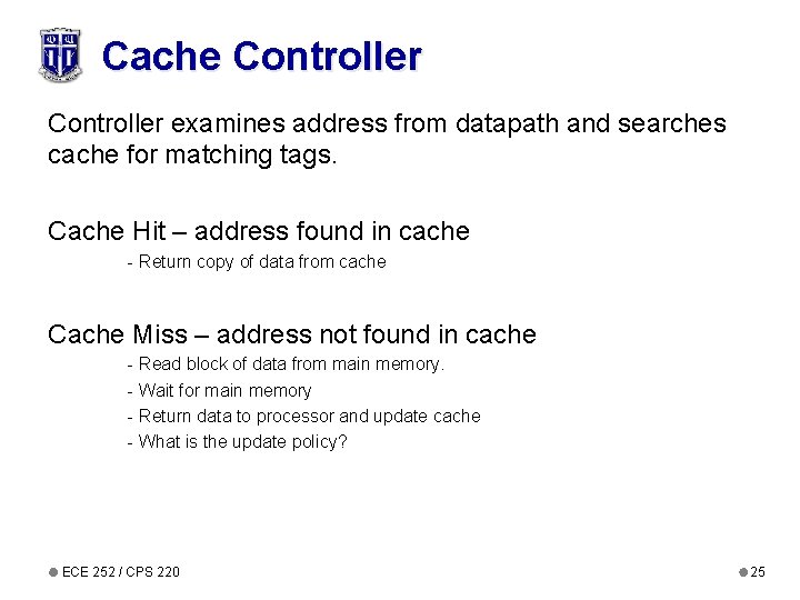
Cache Controller examines address from datapath and searches cache for matching tags. Cache Hit – address found in cache - Return copy of data from cache Cache Miss – address not found in cache - Read block of data from main memory. - Wait for main memory - Return data to processor and update cache - What is the update policy? ECE 252 / CPS 220 24

Cache Controller examines address from datapath and searches cache for matching tags. Cache Hit – address found in cache - Return copy of data from cache Cache Miss – address not found in cache - Read block of data from main memory. - Wait for main memory - Return data to processor and update cache - What is the update policy? ECE 252 / CPS 220 25

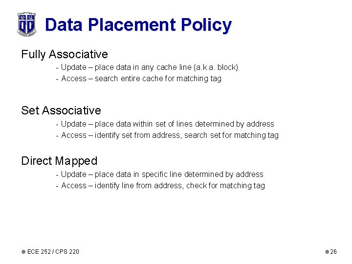
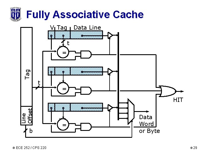
Data Placement Policy Fully Associative - Update – place data in any cache line (a. k. a. block) - Access – search entire cache for matching tag Set Associative - Update – place data within set of lines determined by address - Access – identify set from address, search set for matching tag Direct Mapped - Update – place data in specific line determined by address - Access – identify line from address, check for matching tag ECE 252 / CPS 220 26

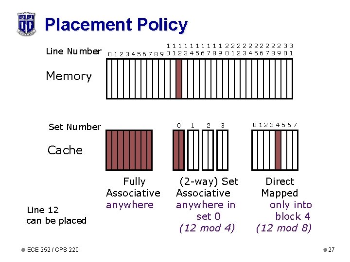
Placement Policy Line Number 11111 22222 33 0123456789 01 Memory Set Number 0 1 2 3 01234567 Cache Line 12 can be placed ECE 252 / CPS 220 Fully Associative anywhere (2 -way) Set Associative anywhere in set 0 (12 mod 4) Direct Mapped only into block 4 (12 mod 8) 27

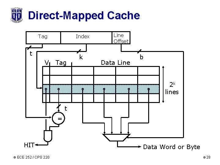
Direct-Mapped Cache Tag Index t V Tag k Line Offset Data Line b 2 k lines t = HIT ECE 252 / CPS 220 Data Word or Byte 28

Fully Associative Cache V Tag Data Line t Tag = t = Line Offset HIT b ECE 252 / CPS 220 = Data Word or Byte 29

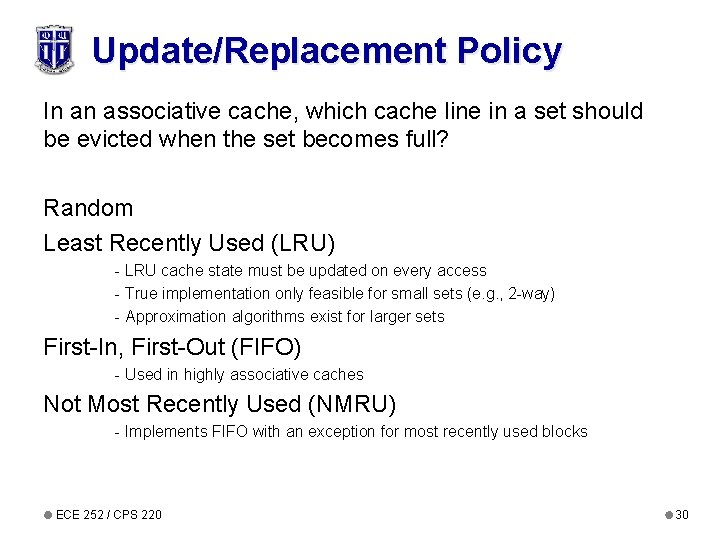
Update/Replacement Policy In an associative cache, which cache line in a set should be evicted when the set becomes full? Random Least Recently Used (LRU) - LRU cache state must be updated on every access - True implementation only feasible for small sets (e. g. , 2 -way) - Approximation algorithms exist for larger sets First-In, First-Out (FIFO) - Used in highly associative caches Not Most Recently Used (NMRU) - Implements FIFO with an exception for most recently used blocks ECE 252 / CPS 220 30

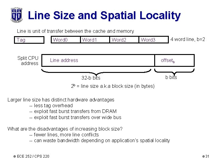
Line Size and Spatial Locality Line is unit of transfer between the cache and memory Tag Split CPU address Word 0 Word 1 Word 2 4 word line, b=2 Word 3 Line address offsetb 32 -b bits 2 b = line size a. k. a block size (in bytes) Larger line size has distinct hardware advantages -- less tag overhead -- exploit fast burst transfers from DRAM -- exploit fast burst transfers over wide bus What are the disadvantages of increasing block size? -- fewer lines, more line conflicts -- can waste bandwidth depending on application’s spatial locality ECE 252 / CPS 220 31

Acknowledgements These slides contain material developed and copyright by - Arvind (MIT) - Krste Asanovic (MIT/UCB) - Joel Emer (Intel/MIT) - James Hoe (CMU) - John Kubiatowicz (UCB) - Alvin Lebeck (Duke) - David Patterson (UCB) - Daniel Sorin (Duke) ECE 252 / CPS 220 32