Duke Compsci 220 ECE 252 Advanced Computer Architecture
![DRAM Basics [Jacob and Wang] • Precharge and Row Access Compsci 220 / ECE DRAM Basics [Jacob and Wang] • Precharge and Row Access Compsci 220 / ECE](https://slidetodoc.com/presentation_image_h2/52e5da7c0a0b1360bec622b25ff30b8f/image-7.jpg)
![Address Translation virtual address[31: 0] physical address[25: 0] VPN[31: 16] translate PPN[27: 16] POFS[15: Address Translation virtual address[31: 0] physical address[25: 0] VPN[31: 16] translate PPN[27: 16] POFS[15:](https://slidetodoc.com/presentation_image_h2/52e5da7c0a0b1360bec622b25ff30b8f/image-31.jpg)
![Multi-Level Page Table • 20 -bit VPN[19: 10] VPN[9: 0] Ø Upper 10 bits Multi-Level Page Table • 20 -bit VPN[19: 10] VPN[9: 0] Ø Upper 10 bits](https://slidetodoc.com/presentation_image_h2/52e5da7c0a0b1360bec622b25ff30b8f/image-35.jpg)
![Cache Size And Page Size [31: 12] VPN [31: 16] ? index [11: 5] Cache Size And Page Size [31: 12] VPN [31: 16] ? index [11: 5]](https://slidetodoc.com/presentation_image_h2/52e5da7c0a0b1360bec622b25ff30b8f/image-47.jpg)
![Stack Smashing via Buffer Overflow int i = 0; char buf[128]; while ((buf[i++] = Stack Smashing via Buffer Overflow int i = 0; char buf[128]; while ((buf[i++] =](https://slidetodoc.com/presentation_image_h2/52e5da7c0a0b1360bec622b25ff30b8f/image-51.jpg)
![Second Memory System Design T (ns) DRAM 10 [31: 30] 20 [31: 30] 30 Second Memory System Design T (ns) DRAM 10 [31: 30] 20 [31: 30] 30](https://slidetodoc.com/presentation_image_h2/52e5da7c0a0b1360bec622b25ff30b8f/image-76.jpg)
- Slides: 91

Duke Compsci 220 /ECE 252 Advanced Computer Architecture I Prof. Alvin R. Lebeck Memory Hierarchy II: Main Memory Slides developed by Amir Roth of University of Pennsylvania with sources that included University of Wisconsin slides by Mark Hill, Guri Sohi, Jim Smith, and David Wood. Slides enhanced by Milo Martin, Mark Hill, Alvin Lebeck, Dan Sorin and David Wood with sources that included Profs. Asanovic, Falsafi, Hoe, Lipasti, Shen, Smith, Sohi, Vijaykumar, and Wood Compsci 220 / ECE 252 (Lebeck): Main Memory 1

Admin • Work on Projects • No Project Presentations (reports only) • Project Status Ø Due Sunday, Nov 14 11: 59 pm (email to me) 3 pgs max. Ø 15% of project grade Ø Details on Web page (see assignments) Reading • Chapter 4 of H&P • Papers on Multicore Compsci 220 / ECE 252 (Lebeck): Main Memory 2

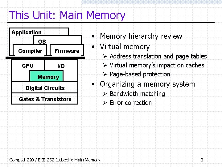
This Unit: Main Memory Application OS Compiler CPU Firmware • Memory hierarchy review • Virtual memory Ø Address translation and page tables Ø Virtual memory’s impact on caches Ø Page-based protection I/O Memory Digital Circuits • Organizing a memory system Gates & Transistors Compsci 220 / ECE 252 (Lebeck): Main Memory Ø Bandwidth matching Ø Error correction 3

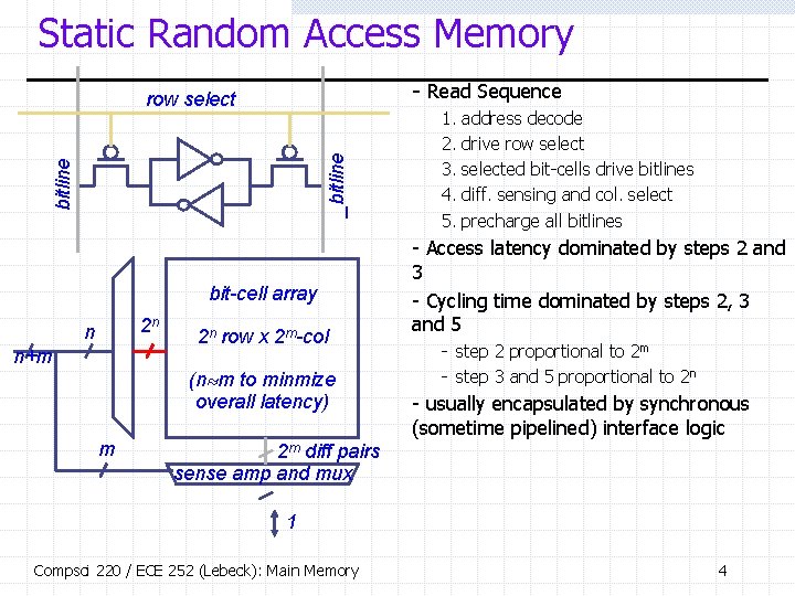
Static Random Access Memory - Read Sequence bitline _bitline row select bit-cell array 2 n n n+m 2 n row x 2 m-col (n m to minmize overall latency) m 1. 2. 3. 4. 5. address decode drive row selected bit-cells drive bitlines diff. sensing and col. select precharge all bitlines - Access latency dominated by steps 2 and 3 - Cycling time dominated by steps 2, 3 and 5 - step 2 proportional to 2 m - step 3 and 5 proportional to 2 n - usually encapsulated by synchronous (sometime pipelined) interface logic 2 m diff pairs sense amp and mux 1 Compsci 220 / ECE 252 (Lebeck): Main Memory 4

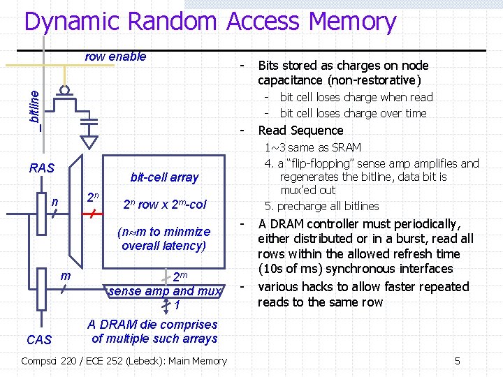
Dynamic Random Access Memory row enable - Bits stored as charges on node capacitance (non-restorative) _bitline - - RAS 2 n 2 n row x 2 m-col (n m to minmize overall latency) m CAS 2 m sense amp and mux 1 Read Sequence 1~3 same as SRAM 4. a “flip-flopping” sense amplifies and regenerates the bitline, data bit is mux’ed out 5. precharge all bitlines bit-cell array n bit cell loses charge when read bit cell loses charge over time - - A DRAM controller must periodically, either distributed or in a burst, read all rows within the allowed refresh time (10 s of ms) synchronous interfaces various hacks to allow faster repeated reads to the same row A DRAM die comprises of multiple such arrays Compsci 220 / ECE 252 (Lebeck): Main Memory 5

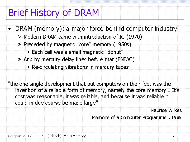
Brief History of DRAM • DRAM (memory): a major force behind computer industry Ø Modern DRAM came with introduction of IC (1970) Ø Preceded by magnetic “core” memory (1950 s) § Each cell was a small magnetic “donut” Ø And by mercury delay lines before that (ENIAC) § Re-circulating vibrations in mercury tubes “the one single development that put computers on their feet was the invention of a reliable form of memory, namely the core memory… It’s cost was reasonable, it was reliable, and because it was reliable it could in due course be made large” Maurice Wilkes Memoirs of a Computer Programmer, 1985 Compsci 220 / ECE 252 (Lebeck): Main Memory 6
![DRAM Basics Jacob and Wang Precharge and Row Access Compsci 220 ECE DRAM Basics [Jacob and Wang] • Precharge and Row Access Compsci 220 / ECE](https://slidetodoc.com/presentation_image_h2/52e5da7c0a0b1360bec622b25ff30b8f/image-7.jpg)
DRAM Basics [Jacob and Wang] • Precharge and Row Access Compsci 220 / ECE 252 (Lebeck): Main Memory 7

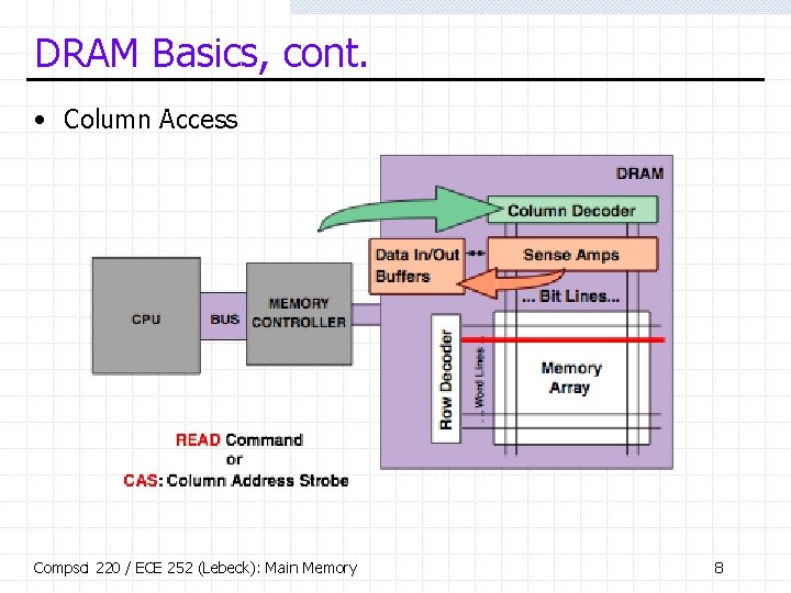
DRAM Basics, cont. • Column Access Compsci 220 / ECE 252 (Lebeck): Main Memory 8

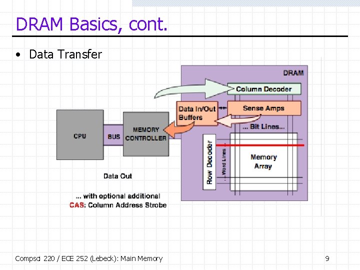
DRAM Basics, cont. • Data Transfer Compsci 220 / ECE 252 (Lebeck): Main Memory 9

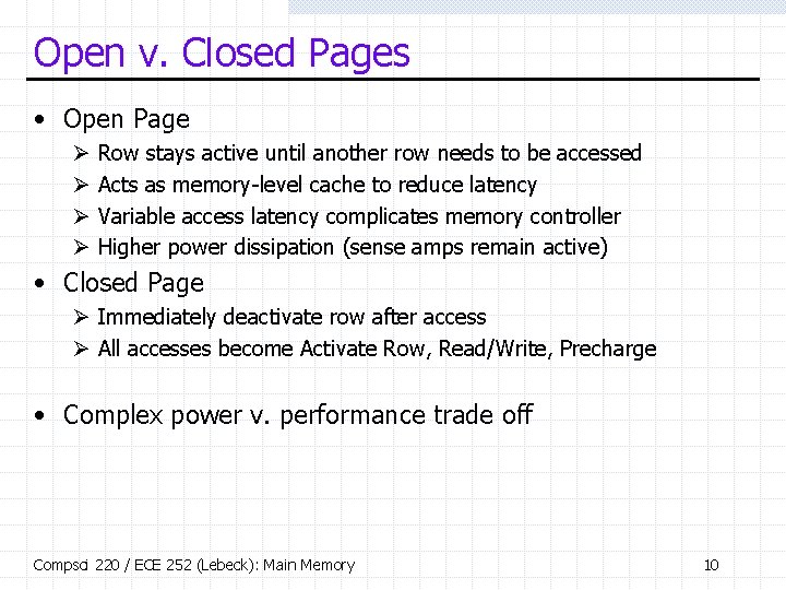
Open v. Closed Pages • Open Page Ø Ø Row stays active until another row needs to be accessed Acts as memory-level cache to reduce latency Variable access latency complicates memory controller Higher power dissipation (sense amps remain active) • Closed Page Ø Immediately deactivate row after access Ø All accesses become Activate Row, Read/Write, Precharge • Complex power v. performance trade off Compsci 220 / ECE 252 (Lebeck): Main Memory 10

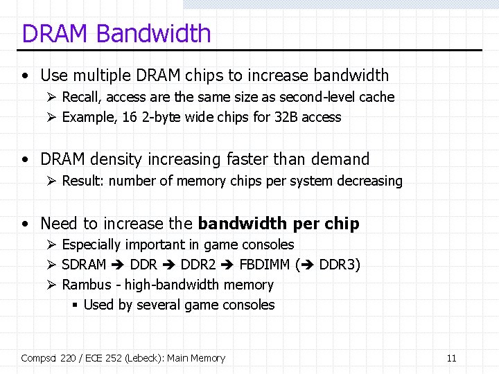
DRAM Bandwidth • Use multiple DRAM chips to increase bandwidth Ø Recall, access are the same size as second-level cache Ø Example, 16 2 -byte wide chips for 32 B access • DRAM density increasing faster than demand Ø Result: number of memory chips per system decreasing • Need to increase the bandwidth per chip Ø Especially important in game consoles Ø SDRAM DDR 2 FBDIMM ( DDR 3) Ø Rambus - high-bandwidth memory § Used by several game consoles Compsci 220 / ECE 252 (Lebeck): Main Memory 11

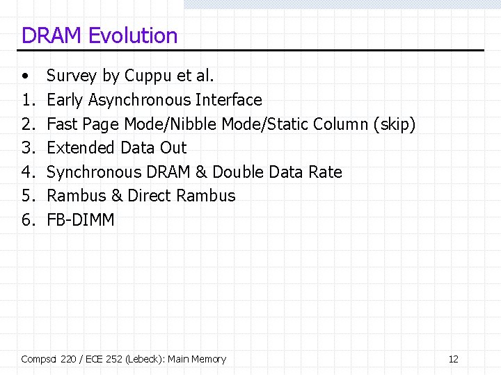
DRAM Evolution • 1. 2. 3. 4. 5. 6. Survey by Cuppu et al. Early Asynchronous Interface Fast Page Mode/Nibble Mode/Static Column (skip) Extended Data Out Synchronous DRAM & Double Data Rate Rambus & Direct Rambus FB-DIMM Compsci 220 / ECE 252 (Lebeck): Main Memory 12

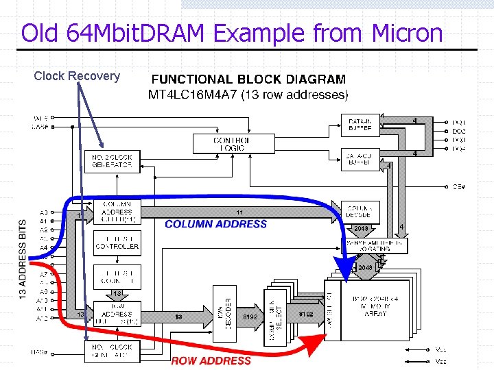
Old 64 Mbit. DRAM Example from Micron Clock Recovery Compsci 220 / ECE 252 (Lebeck): Main Memory 13

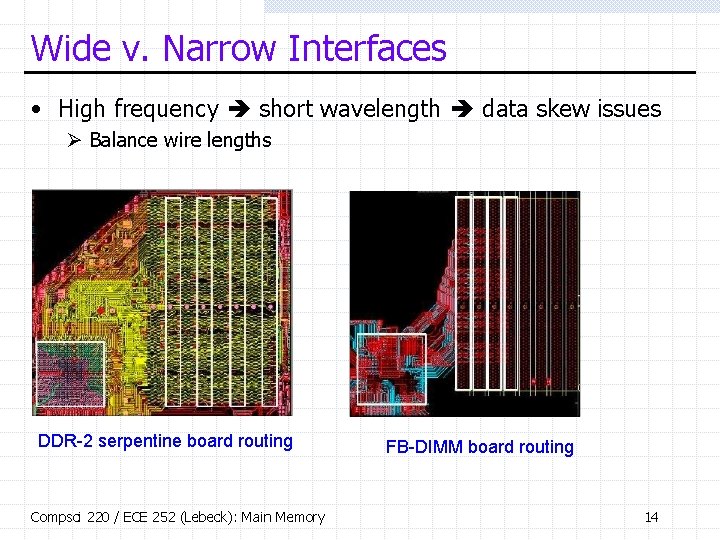
Wide v. Narrow Interfaces • High frequency short wavelength data skew issues Ø Balance wire lengths DDR-2 serpentine board routing Compsci 220 / ECE 252 (Lebeck): Main Memory FB-DIMM board routing 14

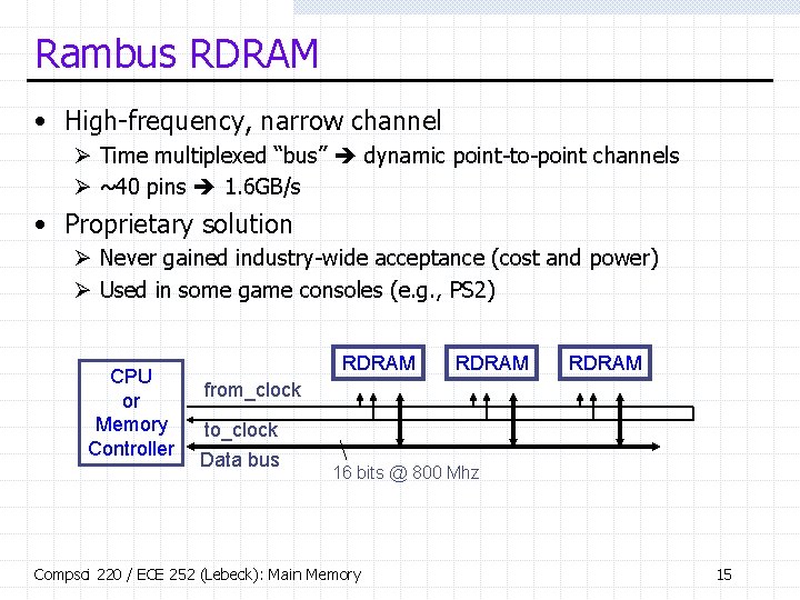
Rambus RDRAM • High-frequency, narrow channel Ø Time multiplexed “bus” dynamic point-to-point channels Ø ~40 pins 1. 6 GB/s • Proprietary solution Ø Never gained industry-wide acceptance (cost and power) Ø Used in some game consoles (e. g. , PS 2) CPU or Memory Controller RDRAM from_clock to_clock Data bus 16 bits @ 800 Mhz Compsci 220 / ECE 252 (Lebeck): Main Memory 15

FB-DIMM Compsci 220 / ECE 252 (Lebeck): Main Memory 16

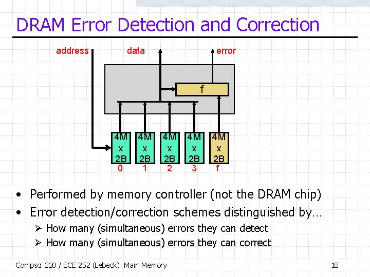
DRAM Reliability • One last thing about DRAM technology… errors Ø DRAM bits can flip from 0 1 or 1 0 § Small charge stored per bit § Energetic -particle strikes disrupt stored charge § Many more bits Ø Modern DRAM systems: built-in error detection/correction § Today all servers; most new desktop and laptops • Key idea: checksum-style redundancy Ø Main DRAM chips store data, additional chips store f(data) § |f(data)| < |data| Ø On read: re-compute f(data), compare with stored f(data) § Different ? Error… Ø Option I (detect): kill program Ø Option II (correct): enough information to fix error? fix and go on Compsci 220 / ECE 252 (Lebeck): Main Memory 17

DRAM Error Detection and Correction address data error f 4 M x 2 B 0 4 M x 2 B 1 4 M x 2 B 2 4 M x 2 B 3 4 M x 2 B f • Performed by memory controller (not the DRAM chip) • Error detection/correction schemes distinguished by… Ø How many (simultaneous) errors they can detect Ø How many (simultaneous) errors they can correct Compsci 220 / ECE 252 (Lebeck): Main Memory 18

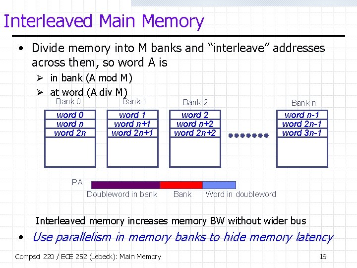
Interleaved Main Memory • Divide memory into M banks and “interleave” addresses across them, so word A is Ø in bank (A mod M) Ø at word (A div M) Bank 0 Bank 1 Bank 2 Bank n word 0 word n word 2 n word 1 word n+1 word 2 word n+2 word 2 n+2 word n-1 word 2 n-1 word 3 n-1 PA Doubleword in bank Bank Word in doubleword Interleaved memory increases memory BW without wider bus • Use parallelism in memory banks to hide memory latency Compsci 220 / ECE 252 (Lebeck): Main Memory 19

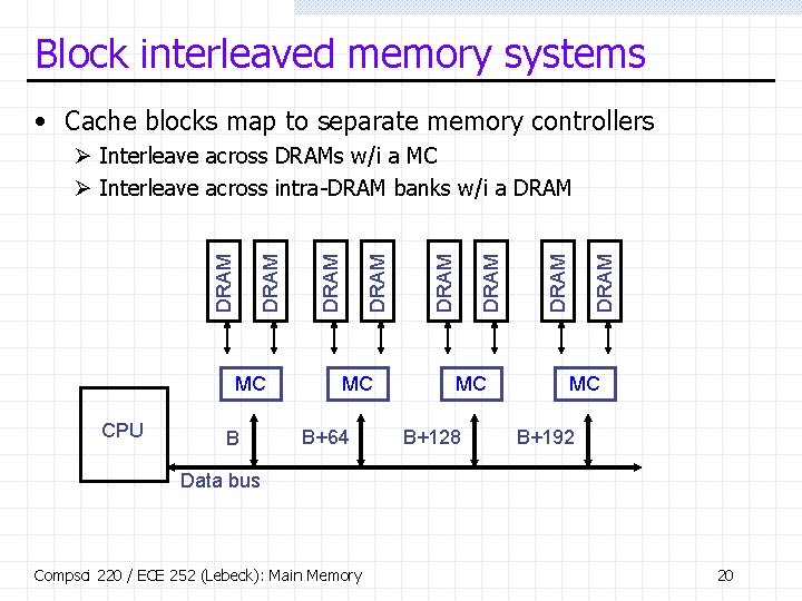
Block interleaved memory systems • Cache blocks map to separate memory controllers MC CPU B MC B+64 MC B+128 DRAM DRAM Ø Interleave across DRAMs w/i a MC Ø Interleave across intra-DRAM banks w/i a DRAM MC B+192 Data bus Compsci 220 / ECE 252 (Lebeck): Main Memory 20

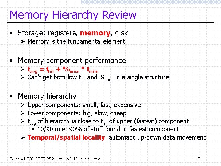
Memory Hierarchy Review • Storage: registers, memory, disk Ø Memory is the fundamental element • Memory component performance Ø tavg = thit + %miss * tmiss Ø Can’t get both low thit and %miss in a single structure • Memory hierarchy Ø Upper components: small, fast, expensive Ø Lower components: big, slow, cheap Ø tavg of hierarchy is close to thit of upper (fastest) component § 10/90 rule: 90% of stuff found in fastest component Ø Temporal/spatial locality: automatic up-down data movement Compsci 220 / ECE 252 (Lebeck): Main Memory 21

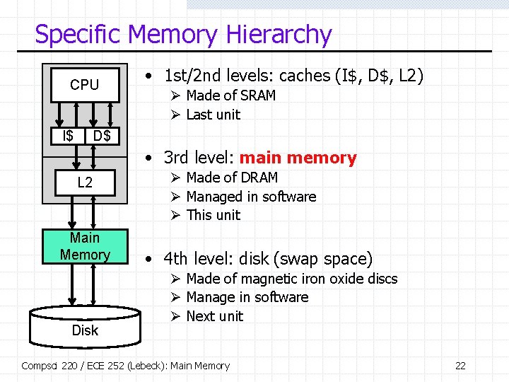
Specific Memory Hierarchy CPU I$ • 1 st/2 nd levels: caches (I$, D$, L 2) Ø Made of SRAM Ø Last unit D$ • 3 rd level: main memory L 2 Main Memory Disk Ø Made of DRAM Ø Managed in software Ø This unit • 4 th level: disk (swap space) Ø Made of magnetic iron oxide discs Ø Manage in software Ø Next unit Compsci 220 / ECE 252 (Lebeck): Main Memory 22

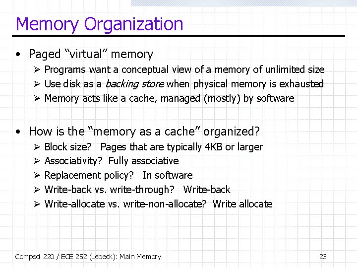
Memory Organization • Paged “virtual” memory Ø Programs want a conceptual view of a memory of unlimited size Ø Use disk as a backing store when physical memory is exhausted Ø Memory acts like a cache, managed (mostly) by software • How is the “memory as a cache” organized? Ø Ø Ø Block size? Pages that are typically 4 KB or larger Associativity? Fully associative Replacement policy? In software Write-back vs. write-through? Write-back Write-allocate vs. write-non-allocate? Write allocate Compsci 220 / ECE 252 (Lebeck): Main Memory 23

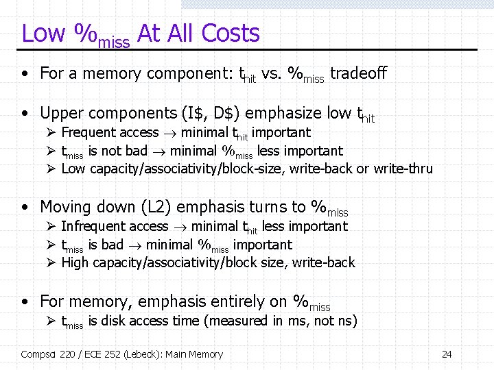
Low %miss At All Costs • For a memory component: thit vs. %miss tradeoff • Upper components (I$, D$) emphasize low thit Ø Frequent access minimal thit important Ø tmiss is not bad minimal %miss less important Ø Low capacity/associativity/block-size, write-back or write-thru • Moving down (L 2) emphasis turns to %miss Ø Infrequent access minimal thit less important Ø tmiss is bad minimal %miss important Ø High capacity/associativity/block size, write-back • For memory, emphasis entirely on %miss Ø tmiss is disk access time (measured in ms, not ns) Compsci 220 / ECE 252 (Lebeck): Main Memory 24

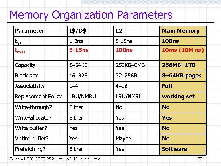
Memory Organization Parameters Parameter I$/D$ L 2 Main Memory thit 1 -2 ns 5 -15 ns 100 ns tmiss 5 -15 ns 100 ns 10 ms (10 M ns) Capacity 8– 64 KB 256 KB– 8 MB 256 MB– 1 TB Block size 16– 32 B 32– 256 B 8– 64 KB pages Associativity 1– 4 4– 16 Full Replacement Policy LRU/NMRU working set Write-through? Either No No Write-allocate? Either Yes Write buffer? Yes No Victim buffer? Yes Maybe No Prefetching? Either Yes Software Compsci 220 / ECE 252 (Lebeck): Main Memory 25

Software Managed Memory • Isn’t full associativity difficult to implement? Ø Yes … in hardware Ø Implement fully associative memory in software • Let’s take a step back… Compsci 220 / ECE 252 (Lebeck): Main Memory 26

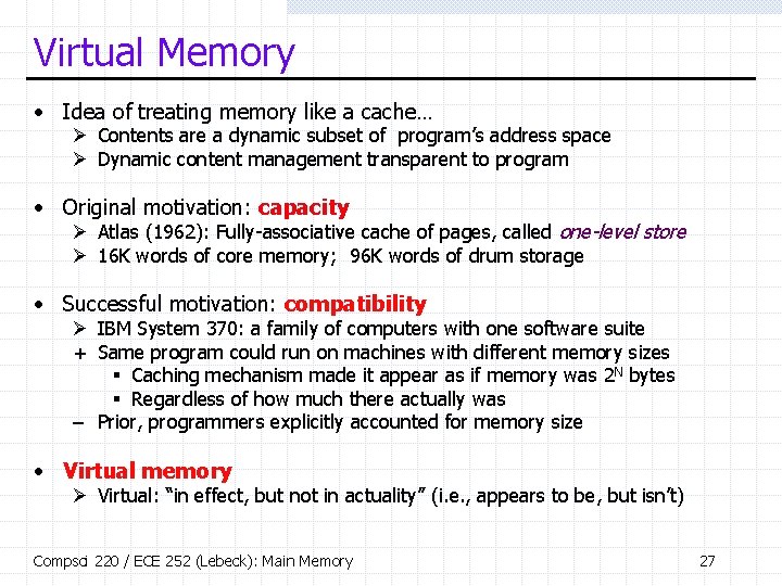
Virtual Memory • Idea of treating memory like a cache… Ø Contents are a dynamic subset of program’s address space Ø Dynamic content management transparent to program • Original motivation: capacity Ø Atlas (1962): Fully-associative cache of pages, called one-level store Ø 16 K words of core memory; 96 K words of drum storage • Successful motivation: compatibility Ø IBM System 370: a family of computers with one software suite + Same program could run on machines with different memory sizes § Caching mechanism made it appear as if memory was 2 N bytes § Regardless of how much there actually was – Prior, programmers explicitly accounted for memory size • Virtual memory Ø Virtual: “in effect, but not in actuality” (i. e. , appears to be, but isn’t) Compsci 220 / ECE 252 (Lebeck): Main Memory 27

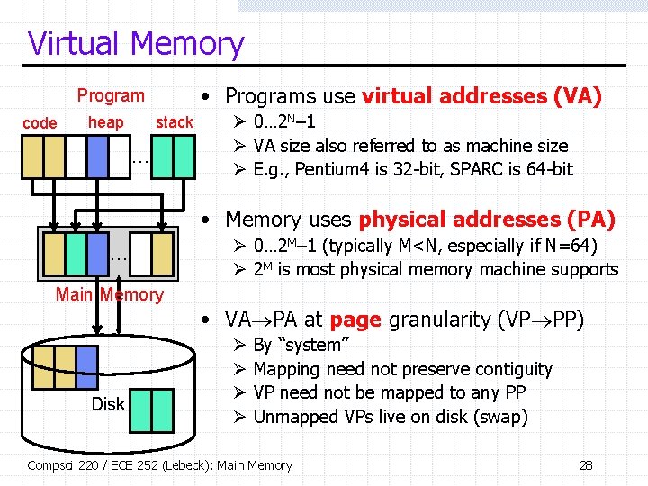
Virtual Memory • Programs use virtual addresses (VA) Program code heap stack … Ø 0… 2 N– 1 Ø VA size also referred to as machine size Ø E. g. , Pentium 4 is 32 -bit, SPARC is 64 -bit • Memory uses physical addresses (PA) … Ø 0… 2 M– 1 (typically M<N, especially if N=64) Ø 2 M is most physical memory machine supports Main Memory • VA PA at page granularity (VP PP) Disk Ø Ø By “system” Mapping need not preserve contiguity VP need not be mapped to any PP Unmapped VPs live on disk (swap) Compsci 220 / ECE 252 (Lebeck): Main Memory 28

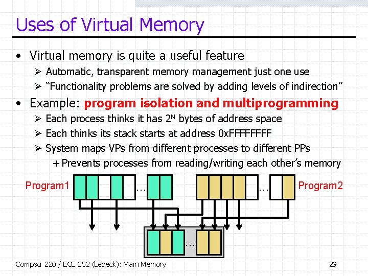
Uses of Virtual Memory • Virtual memory is quite a useful feature Ø Automatic, transparent memory management just one use Ø “Functionality problems are solved by adding levels of indirection” • Example: program isolation and multiprogramming Ø Each process thinks it has 2 N bytes of address space Ø Each thinks its stack starts at address 0 x. FFFF Ø System maps VPs from different processes to different PPs + Prevents processes from reading/writing each other’s memory Program 1 … … Program 2 … Compsci 220 / ECE 252 (Lebeck): Main Memory 29

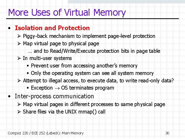
More Uses of Virtual Memory • Isolation and Protection Ø Piggy-back mechanism to implement page-level protection Ø Map virtual page to physical page … and to Read/Write/Execute protection bits in page table Ø In multi-user systems § Prevent user from accessing another’s memory § Only the operating system can see all system memory Ø Attempt to illegal access, to execute data, to write read-only data? § Exception OS terminates program • Inter-process communication Ø Map virtual pages in different processes to same physical page Ø Share files via the UNIX mmap() call Compsci 220 / ECE 252 (Lebeck): Main Memory 30
![Address Translation virtual address31 0 physical address25 0 VPN31 16 translate PPN27 16 POFS15 Address Translation virtual address[31: 0] physical address[25: 0] VPN[31: 16] translate PPN[27: 16] POFS[15:](https://slidetodoc.com/presentation_image_h2/52e5da7c0a0b1360bec622b25ff30b8f/image-31.jpg)
Address Translation virtual address[31: 0] physical address[25: 0] VPN[31: 16] translate PPN[27: 16] POFS[15: 0] don’t touch POFS[15: 0] • VA PA mapping called address translation Ø Ø Split VA into virtual page number (VPN) and page offset (POFS) Translate VPN into physical page number (PPN) POFS is not translated VA PA = [VPN, POFS] [PPN, POFS] • Example above Ø 64 KB pages 16 -bit POFS Ø 32 -bit machine 32 -bit VA 16 -bit VPN Ø Maximum 256 MB memory 28 -bit PA 12 -bit PPN Compsci 220 / ECE 252 (Lebeck): Main Memory 31

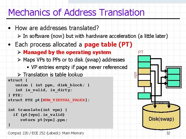
Mechanics of Address Translation • How are addresses translated? Ø In software (now) but with hardware acceleration (a little later) • Each process allocated a page table (PT) struct { union { int ppn, disk_block; } int is_valid, is_dirty; } PTE; struct PTE pt[NUM_VIRTUAL_PAGES]; int translate(int vpn) { if (pt[vpn]. is_valid) return pt[vpn]. ppn; } Compsci 220 / ECE 252 (Lebeck): Main Memory PT vpn Ø Managed by the operating system Ø Maps VPs to PPs or to disk (swap) addresses § VP entries empty if page never referenced Ø Translation is table lookup Disk(swap) 32

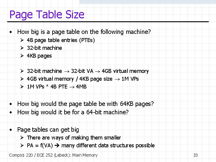
Page Table Size • How big is a page table on the following machine? Ø 4 B page table entries (PTEs) Ø 32 -bit machine Ø 4 KB pages Ø 32 -bit machine 32 -bit VA 4 GB virtual memory Ø 4 GB virtual memory / 4 KB page size 1 M VPs Ø 1 M VPs * 4 B PTE 4 MB • How big would the page table be with 64 KB pages? • How big would it be for a 64 -bit machine? • Page tables can get big Ø There are ways of making them smaller Ø PA = f(VA) many different data structures possible Compsci 220 / ECE 252 (Lebeck): Main Memory 33

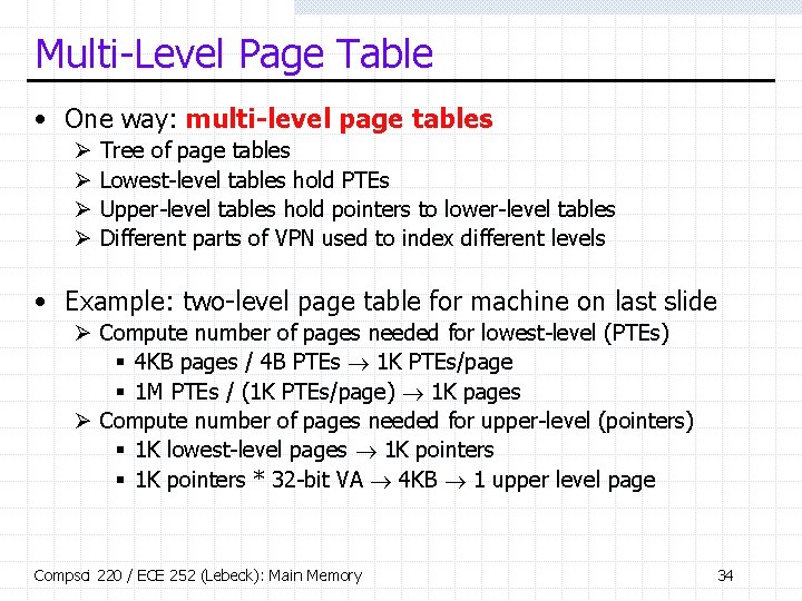
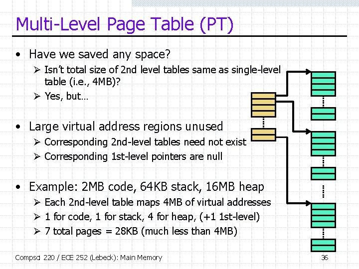
Multi-Level Page Table • One way: multi-level page tables Ø Ø Tree of page tables Lowest-level tables hold PTEs Upper-level tables hold pointers to lower-level tables Different parts of VPN used to index different levels • Example: two-level page table for machine on last slide Ø Compute number of pages needed for lowest-level (PTEs) § 4 KB pages / 4 B PTEs 1 K PTEs/page § 1 M PTEs / (1 K PTEs/page) 1 K pages Ø Compute number of pages needed for upper-level (pointers) § 1 K lowest-level pages 1 K pointers § 1 K pointers * 32 -bit VA 4 KB 1 upper level page Compsci 220 / ECE 252 (Lebeck): Main Memory 34
![MultiLevel Page Table 20 bit VPN19 10 VPN9 0 Ø Upper 10 bits Multi-Level Page Table • 20 -bit VPN[19: 10] VPN[9: 0] Ø Upper 10 bits](https://slidetodoc.com/presentation_image_h2/52e5da7c0a0b1360bec622b25ff30b8f/image-35.jpg)
Multi-Level Page Table • 20 -bit VPN[19: 10] VPN[9: 0] Ø Upper 10 bits index 1 st-level table 1 st-level Ø Lower 10 bits index 2 nd-level table pt “root” “pointers” 2 nd-level PTEs struct { union { int ppn, disk_block; } int is_valid, is_dirty; } PTE; struct { struct PTE ptes[1024]; } L 2 PT; struct L 2 PT *pt[1024]; int translate(int vpn) { struct L 2 PT *l 2 pt = pt[vpn>>10]; if (l 2 pt && l 2 pt->ptes[vpn&1023]. is_valid) return l 2 pt->ptes[vpn&1023]. ppn; } Compsci 220 / ECE 252 (Lebeck): Main Memory 35

Multi-Level Page Table (PT) • Have we saved any space? Ø Isn’t total size of 2 nd level tables same as single-level table (i. e. , 4 MB)? Ø Yes, but… • Large virtual address regions unused Ø Corresponding 2 nd-level tables need not exist Ø Corresponding 1 st-level pointers are null • Example: 2 MB code, 64 KB stack, 16 MB heap Ø Each 2 nd-level table maps 4 MB of virtual addresses Ø 1 for code, 1 for stack, 4 for heap, (+1 1 st-level) Ø 7 total pages = 28 KB (much less than 4 MB) Compsci 220 / ECE 252 (Lebeck): Main Memory 36

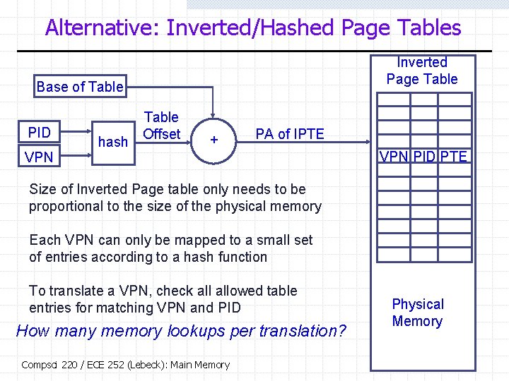
Alternative: Inverted/Hashed Page Tables Inverted Page Table Base of Table PID VPN hash Table Offset + PA of IPTE VPN PID PTE Size of Inverted Page table only needs to be proportional to the size of the physical memory Each VPN can only be mapped to a small set of entries according to a hash function To translate a VPN, check allowed table entries for matching VPN and PID How many memory lookups per translation? Compsci 220 / ECE 252 (Lebeck): Main Memory Physical Memory 37

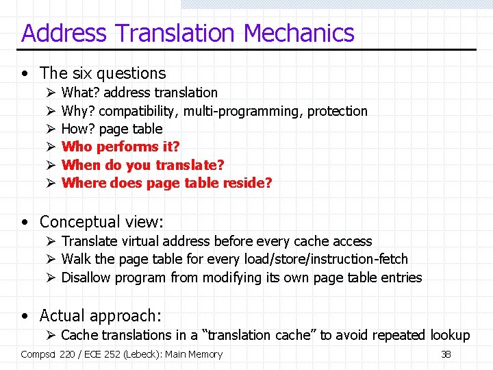
Address Translation Mechanics • The six questions Ø Ø Ø What? address translation Why? compatibility, multi-programming, protection How? page table Who performs it? When do you translate? Where does page table reside? • Conceptual view: Ø Translate virtual address before every cache access Ø Walk the page table for every load/store/instruction-fetch Ø Disallow program from modifying its own page table entries • Actual approach: Ø Cache translations in a “translation cache” to avoid repeated lookup Compsci 220 / ECE 252 (Lebeck): Main Memory 38

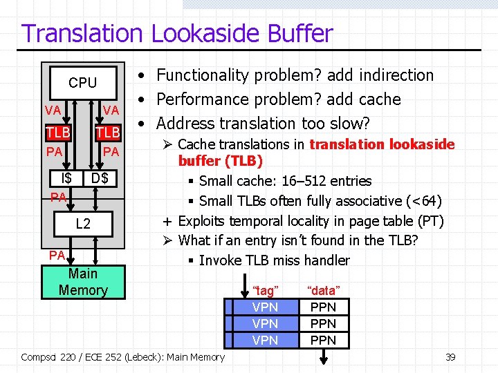
Translation Lookaside Buffer CPU VA VA TLB PA PA I$ D$ PA L 2 PA Main Memory • Functionality problem? add indirection • Performance problem? add cache • Address translation too slow? Ø Cache translations in translation lookaside buffer (TLB) § Small cache: 16– 512 entries § Small TLBs often fully associative (<64) + Exploits temporal locality in page table (PT) Ø What if an entry isn’t found in the TLB? § Invoke TLB miss handler Compsci 220 / ECE 252 (Lebeck): Main Memory “tag” VPN VPN “data” PPN PPN 39

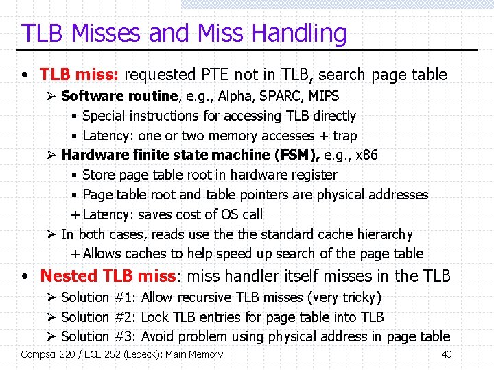
TLB Misses and Miss Handling • TLB miss: requested PTE not in TLB, search page table Ø Software routine, e. g. , Alpha, SPARC, MIPS § Special instructions for accessing TLB directly § Latency: one or two memory accesses + trap Ø Hardware finite state machine (FSM), e. g. , x 86 § Store page table root in hardware register § Page table root and table pointers are physical addresses + Latency: saves cost of OS call Ø In both cases, reads use the standard cache hierarchy + Allows caches to help speed up search of the page table • Nested TLB miss: miss handler itself misses in the TLB Ø Solution #1: Allow recursive TLB misses (very tricky) Ø Solution #2: Lock TLB entries for page table into TLB Ø Solution #3: Avoid problem using physical address in page table Compsci 220 / ECE 252 (Lebeck): Main Memory 40

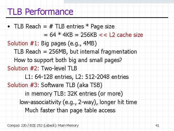
TLB Performance • TLB Reach = # TLB entries * Page size = 64 * 4 KB = 256 KB << L 2 cache size Solution #1: Big pages (e. g. , 4 MB) TLB Reach = 256 MB, but internal fragmentation How to support both big and small pages? Solution #2: Two-level TLB L 1: 64 -128 entries, L 2: 512 -2048 entries Solution #3: Software TLB (aka TSB) in memory TLB: 32 K entries (or more) low-associativity (e. g. , 2 -way), longer hit time Much faster than page table access Compsci 220 / ECE 252 (Lebeck): Main Memory 41

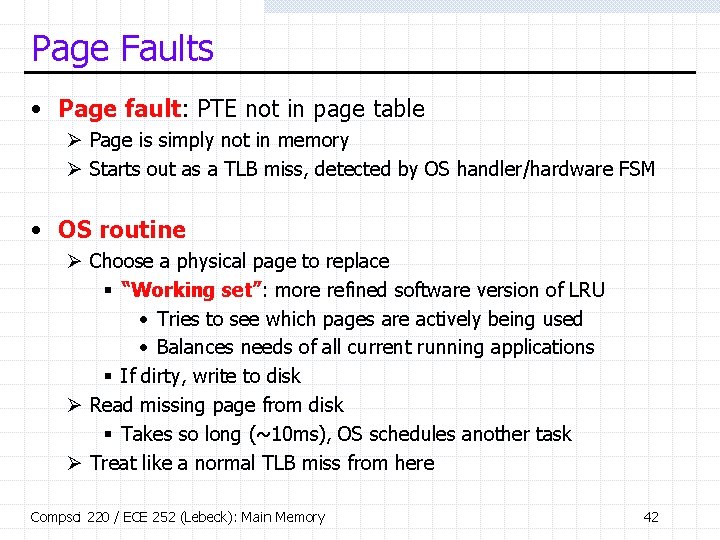
Page Faults • Page fault: PTE not in page table Ø Page is simply not in memory Ø Starts out as a TLB miss, detected by OS handler/hardware FSM • OS routine Ø Choose a physical page to replace § “Working set”: more refined software version of LRU • Tries to see which pages are actively being used • Balances needs of all current running applications § If dirty, write to disk Ø Read missing page from disk § Takes so long (~10 ms), OS schedules another task Ø Treat like a normal TLB miss from here Compsci 220 / ECE 252 (Lebeck): Main Memory 42

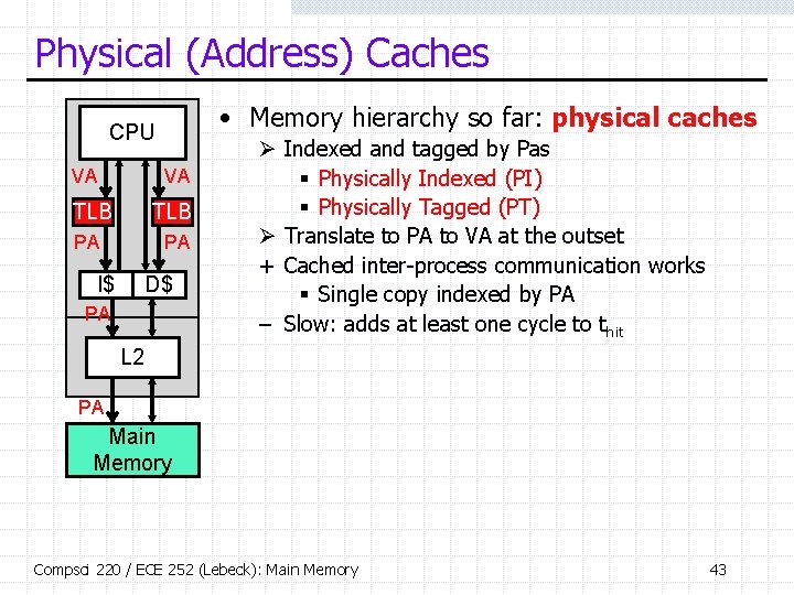
Physical (Address) Caches • Memory hierarchy so far: physical caches CPU VA VA TLB PA PA I$ D$ PA Ø Indexed and tagged by Pas § Physically Indexed (PI) § Physically Tagged (PT) Ø Translate to PA to VA at the outset + Cached inter-process communication works § Single copy indexed by PA – Slow: adds at least one cycle to thit L 2 PA Main Memory Compsci 220 / ECE 252 (Lebeck): Main Memory 43

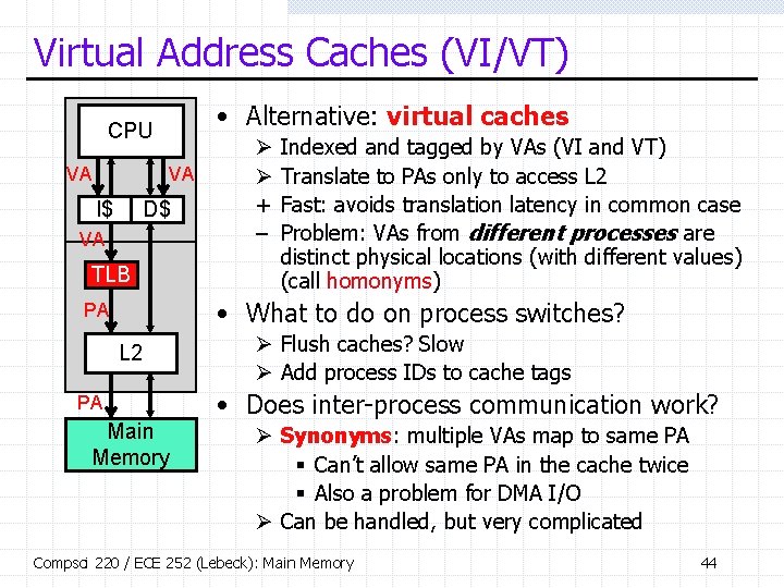
Virtual Address Caches (VI/VT) • Alternative: virtual caches CPU VA VA I$ D$ VA TLB Ø Ø + – Indexed and tagged by VAs (VI and VT) Translate to PAs only to access L 2 Fast: avoids translation latency in common case Problem: VAs from different processes are distinct physical locations (with different values) (call homonyms) • What to do on process switches? PA L 2 PA Main Memory Ø Flush caches? Slow Ø Add process IDs to cache tags • Does inter-process communication work? Ø Synonyms: multiple VAs map to same PA § Can’t allow same PA in the cache twice § Also a problem for DMA I/O Ø Can be handled, but very complicated Compsci 220 / ECE 252 (Lebeck): Main Memory 44

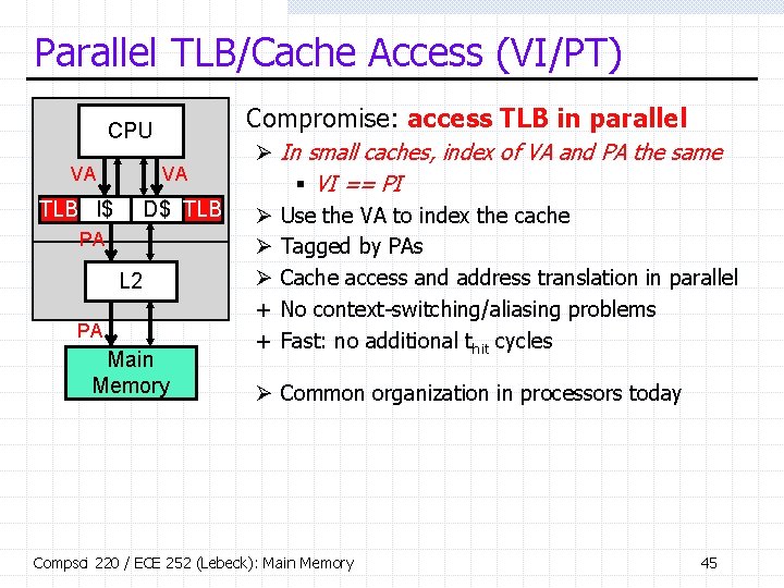
Parallel TLB/Cache Access (VI/PT) • Compromise: access TLB in parallel CPU VA VA TLB I$ D$ TLB PA L 2 PA Main Memory Ø In small caches, index of VA and PA the same § VI == PI Ø Use the VA to index the cache Ø Tagged by PAs Ø Cache access and address translation in parallel + No context-switching/aliasing problems + Fast: no additional thit cycles Ø Common organization in processors today Compsci 220 / ECE 252 (Lebeck): Main Memory 45

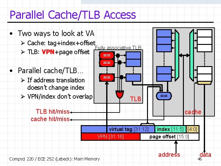
Parallel Cache/TLB Access • Two ways to look at VA Ø Cache: tag+index+offset Fully associative TLB Ø TLB: VPN+page offset == == • Parallel cache/TLB… == Ø If address translation doesn’t change index Ø VPN/index don’t overlap TLB == TLB hit/miss cache virtual tag [31: 12] index [11: 5] [4: 0] VPN [31: 16] page offset [15: 0] Compsci 220 / ECE 252 (Lebeck): Main Memory address data 46
![Cache Size And Page Size 31 12 VPN 31 16 index 11 5 Cache Size And Page Size [31: 12] VPN [31: 16] ? index [11: 5]](https://slidetodoc.com/presentation_image_h2/52e5da7c0a0b1360bec622b25ff30b8f/image-47.jpg)
Cache Size And Page Size [31: 12] VPN [31: 16] ? index [11: 5] [4: 0] page offset [15: 0] • Relationship between page size and L 1 cache size Ø Forced by non-overlap between VPN and IDX portions of VA § Which is required for TLB access Ø Rule: (cache size) / (associativity) ≤ page size Ø Result: associativity increases allowable cache sizes Ø Systems are moving towards bigger (64 KB) pages § To use parallel translation with bigger caches § To amortize disk latency Ø Example: Pentium 4, 4 KB pages, 8 KB, 2 -way SA L 1 data cache • If cache is too big, same issues as virtually-indexed caches Ø Other tricks can help (e. g. , set-associative main memory) Compsci 220 / ECE 252 (Lebeck): Main Memory 47

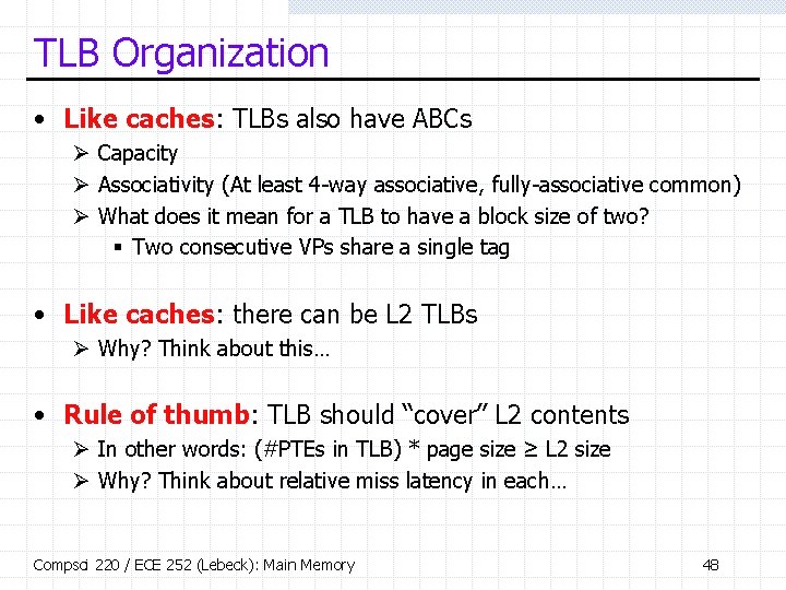
TLB Organization • Like caches: TLBs also have ABCs Ø Capacity Ø Associativity (At least 4 -way associative, fully-associative common) Ø What does it mean for a TLB to have a block size of two? § Two consecutive VPs share a single tag • Like caches: there can be L 2 TLBs Ø Why? Think about this… • Rule of thumb: TLB should “cover” L 2 contents Ø In other words: (#PTEs in TLB) * page size ≥ L 2 size Ø Why? Think about relative miss latency in each… Compsci 220 / ECE 252 (Lebeck): Main Memory 48

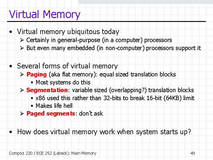
Virtual Memory • Virtual memory ubiquitous today Ø Certainly in general-purpose (in a computer) processors Ø But even many embedded (in non-computer) processors support it • Several forms of virtual memory Ø Paging (aka flat memory): equal sized translation blocks § Most systems do this Ø Segmentation: variable sized (overlapping? ) translation blocks § x 86 used this rather than 32 -bits to break 16 -bit (64 KB) limit § Makes life hell Ø Paged segments: don’t ask • How does virtual memory work when system starts up? Compsci 220 / ECE 252 (Lebeck): Main Memory 49

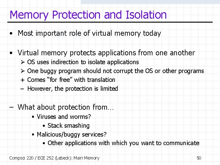
Memory Protection and Isolation • Most important role of virtual memory today • Virtual memory protects applications from one another Ø Ø + – OS uses indirection to isolate applications One buggy program should not corrupt the OS or other programs Comes “for free” with translation However, the protection is limited – What about protection from… § Viruses and worms? • Stack smashing § Malicious/buggy services? • Other applications with which you want to communicate Compsci 220 / ECE 252 (Lebeck): Main Memory 50
![Stack Smashing via Buffer Overflow int i 0 char buf128 while bufi Stack Smashing via Buffer Overflow int i = 0; char buf[128]; while ((buf[i++] =](https://slidetodoc.com/presentation_image_h2/52e5da7c0a0b1360bec622b25ff30b8f/image-51.jpg)
Stack Smashing via Buffer Overflow int i = 0; char buf[128]; while ((buf[i++] = getc()) != ’n’) ; return; • Stack smashing via buffer overflow Ø Ø Oldest trick in the virus book Exploits stack frame layout and… Sloppy code: length-unchecked copy to stack buffer “Attack string”: code (128 B) + &buf[0] (4 B) Ø Caller return address replaced with pointer to attack code § Caller return… § …executes attack code at caller’s privilege level Ø Vulnerable programs: gzip-1. 2. 4, sendmail-8. 7. 5 ra buf[128] ra &buf[0] attack code ra Compsci 220 / ECE 252 (Lebeck): Main Memory 51

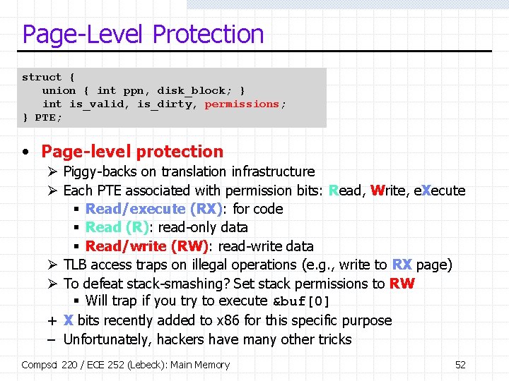
Page-Level Protection struct { union { int ppn, disk_block; } int is_valid, is_dirty, permissions; } PTE; • Page-level protection Ø Piggy-backs on translation infrastructure Ø Each PTE associated with permission bits: Read, Write, e. Xecute § Read/execute (RX): for code § Read (R): read-only data § Read/write (RW): read-write data Ø TLB access traps on illegal operations (e. g. , write to RX page) Ø To defeat stack-smashing? Set stack permissions to RW § Will trap if you try to execute &buf[0] + X bits recently added to x 86 for this specific purpose – Unfortunately, hackers have many other tricks Compsci 220 / ECE 252 (Lebeck): Main Memory 52

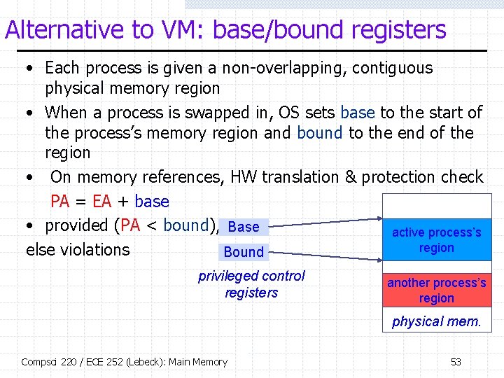
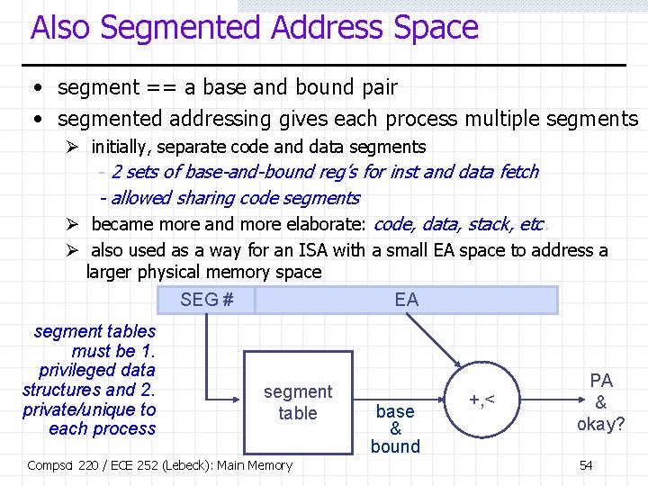
Alternative to VM: base/bound registers • Each process is given a non-overlapping, contiguous physical memory region • When a process is swapped in, OS sets base to the start of the process’s memory region and bound to the end of the region • On memory references, HW translation & protection check PA = EA + base • provided (PA < bound), Base active process’s region else violations Bound privileged control registers another process’s region physical mem. Compsci 220 / ECE 252 (Lebeck): Main Memory 53

Also Segmented Address Space • segment == a base and bound pair • segmented addressing gives each process multiple segments Ø initially, separate code and data segments - 2 sets of base-and-bound reg’s for inst and data fetch - allowed sharing code segments Ø became more and more elaborate: code, data, stack, etc. Ø also used as a way for an ISA with a small EA space to address a larger physical memory space SEG # segment tables must be 1. privileged data structures and 2. private/unique to each process EA segment table Compsci 220 / ECE 252 (Lebeck): Main Memory base & bound +, < PA & okay? 54

Backups Compsci 220 / ECE 252 (Lebeck): Main Memory 55

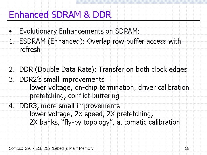
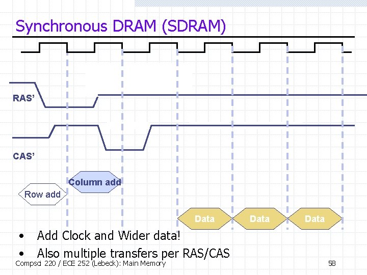
Enhanced SDRAM & DDR • Evolutionary Enhancements on SDRAM: 1. ESDRAM (Enhanced): Overlap row buffer access with refresh 2. DDR (Double Data Rate): Transfer on both clock edges 3. DDR 2’s small improvements lower voltage, on-chip termination, driver calibration prefetching, conflict buffering 4. DDR 3, more small improvements lower voltage, 2 X speed, 2 X prefetching, 2 X banks, “fly-by topology”, automatic calibration Compsci 220 / ECE 252 (Lebeck): Main Memory 56

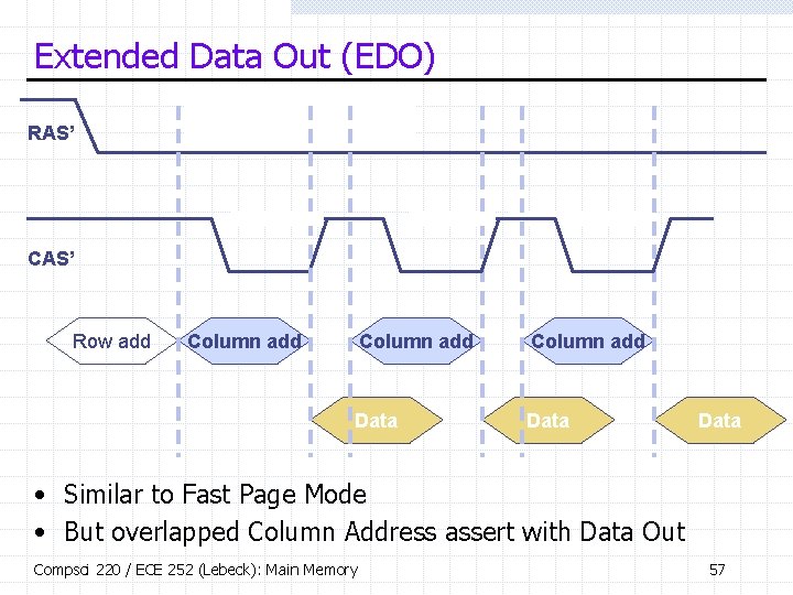
Extended Data Out (EDO) RAS’ CAS’ Row add Column add Data • Similar to Fast Page Mode • But overlapped Column Address assert with Data Out Compsci 220 / ECE 252 (Lebeck): Main Memory 57

Synchronous DRAM (SDRAM) RAS’ Column add Row add Data • • Add Clock and Wider data! Also multiple transfers per RAS/CAS Compsci 220 / ECE 252 (Lebeck): Main Memory Data 58

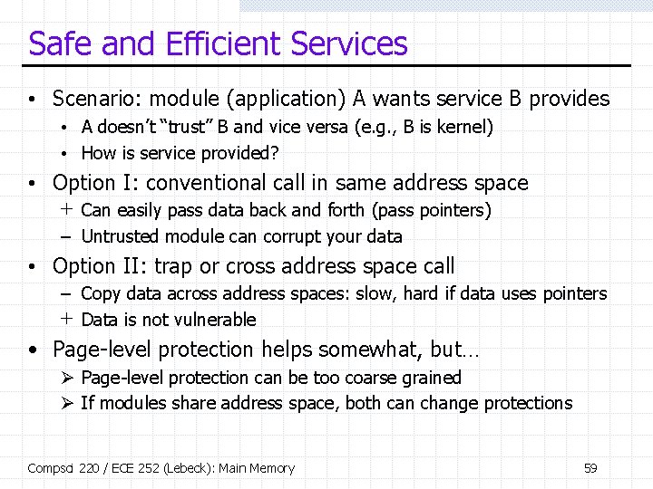
Safe and Efficient Services • Scenario: module (application) A wants service B provides • A doesn’t “trust” B and vice versa (e. g. , B is kernel) • How is service provided? • Option I: conventional call in same address space + Can easily pass data back and forth (pass pointers) – Untrusted module can corrupt your data • Option II: trap or cross address space call – Copy data across address spaces: slow, hard if data uses pointers + Data is not vulnerable • Page-level protection helps somewhat, but… Ø Page-level protection can be too coarse grained Ø If modules share address space, both can change protections Compsci 220 / ECE 252 (Lebeck): Main Memory 59

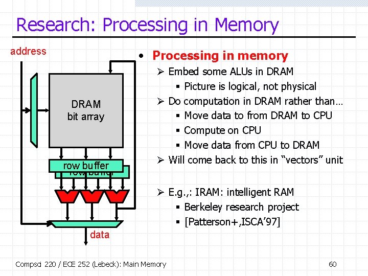
Research: Processing in Memory address • Processing in memory DRAM bit array row buffer Ø Embed some ALUs in DRAM § Picture is logical, not physical Ø Do computation in DRAM rather than… § Move data to from DRAM to CPU § Compute on CPU § Move data from CPU to DRAM Ø Will come back to this in “vectors” unit Ø E. g. , : IRAM: intelligent RAM § Berkeley research project § [Patterson+, ISCA’ 97] data Compsci 220 / ECE 252 (Lebeck): Main Memory 60

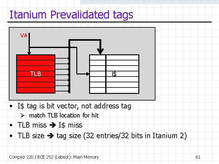
Itanium Prevalidated tags VA TLB I$ • I$ tag is bit vector, not address tag Ø match TLB location for hit • TLB miss I$ miss • TLB size tag size (32 entries/32 bits in Itanium 2) Compsci 220 / ECE 252 (Lebeck): Main Memory 61

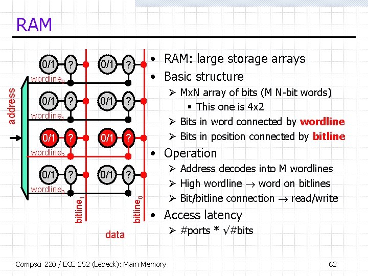
RAM 0/1 ? 0/1 • RAM: large storage arrays • Basic structure ? address wordline 0 0/1 ? ? 0/1 ? Ø Mx. N array of bits (M N-bit words) § This one is 4 x 2 Ø Bits in word connected by wordline Ø Bits in position connected by bitline wordline 1 0/1 • Operation wordline 2 0/1 ? 0/1 Ø Address decodes into M wordlines Ø High wordline word on bitlines Ø Bit/bitline connection read/write ? bitline 0 bitline 1 wordline 3 • Access latency data Compsci 220 / ECE 252 (Lebeck): Main Memory Ø #ports * √#bits 62

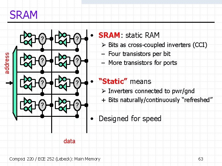
address SRAM ? ? • SRAM: static RAM Ø Bits as cross-coupled inverters (CCI) – Four transistors per bit – More transistors for ports • “Static” means Ø Inverters connected to pwr/gnd + Bits naturally/continuously “refreshed” ? • Designed for speed data Compsci 220 / ECE 252 (Lebeck): Main Memory 63

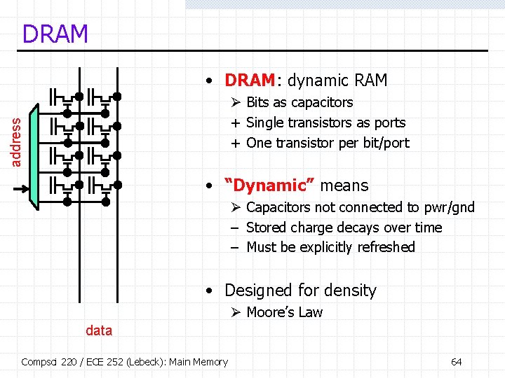
DRAM • DRAM: dynamic RAM address Ø Bits as capacitors + Single transistors as ports + One transistor per bit/port • “Dynamic” means Ø Capacitors not connected to pwr/gnd – Stored charge decays over time – Must be explicitly refreshed • Designed for density Ø Moore’s Law data Compsci 220 / ECE 252 (Lebeck): Main Memory 64

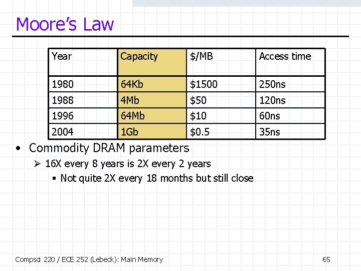
Moore’s Law Year Capacity $/MB Access time 1980 64 Kb $1500 250 ns 1988 4 Mb $50 120 ns 1996 64 Mb $10 60 ns 2004 1 Gb $0. 5 35 ns • Commodity DRAM parameters Ø 16 X every 8 years is 2 X every 2 years § Not quite 2 X every 18 months but still close Compsci 220 / ECE 252 (Lebeck): Main Memory 65

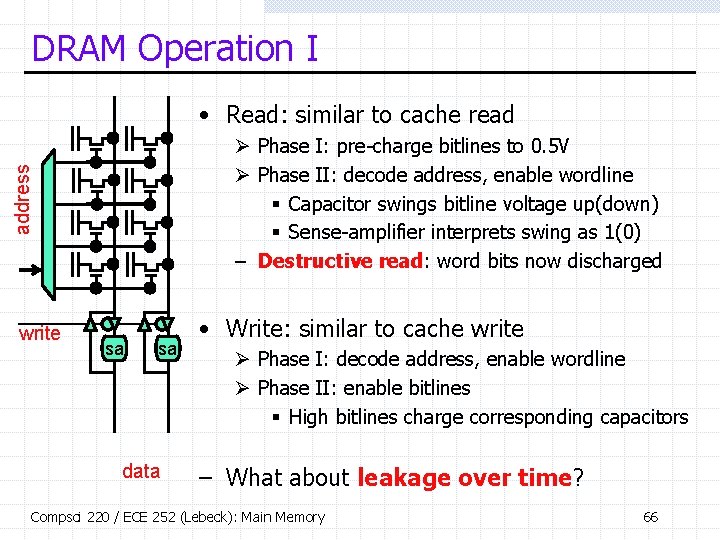
DRAM Operation I • Read: similar to cache read address Ø Phase I: pre-charge bitlines to 0. 5 V Ø Phase II: decode address, enable wordline § Capacitor swings bitline voltage up(down) § Sense-amplifier interprets swing as 1(0) – Destructive read: word bits now discharged write sa sa data • Write: similar to cache write Ø Phase I: decode address, enable wordline Ø Phase II: enable bitlines § High bitlines charge corresponding capacitors – What about leakage over time? Compsci 220 / ECE 252 (Lebeck): Main Memory 66

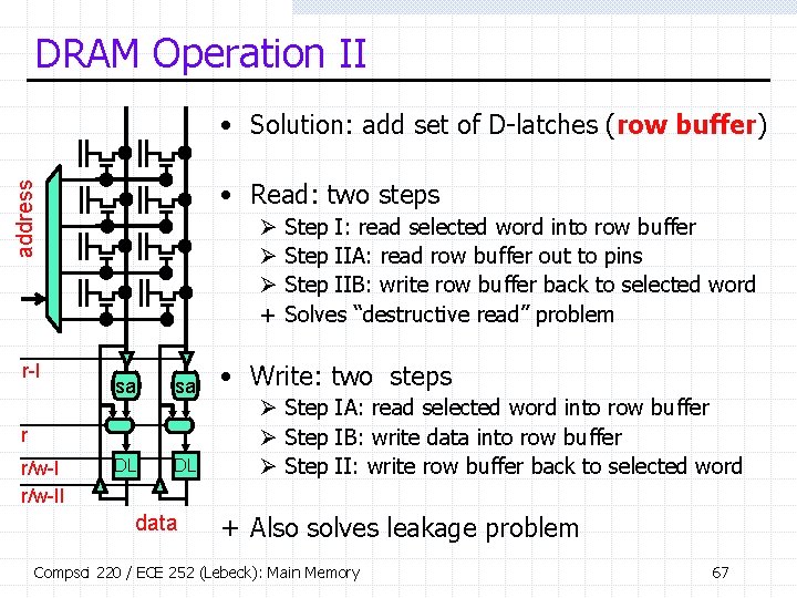
DRAM Operation II • Solution: add set of D-latches (row buffer) address • Read: two steps r-I Ø Ø Ø + sa sa DL DL r r/w-II data Step I: read selected word into row buffer Step IIA: read row buffer out to pins Step IIB: write row buffer back to selected word Solves “destructive read” problem • Write: two steps Ø Step IA: read selected word into row buffer Ø Step IB: write data into row buffer Ø Step II: write row buffer back to selected word + Also solves leakage problem Compsci 220 / ECE 252 (Lebeck): Main Memory 67

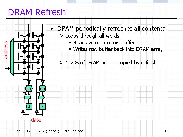
DRAM Refresh • DRAM periodically refreshes all contents address Ø Loops through all words § Reads word into row buffer § Writes row buffer back into DRAM array Ø 1– 2% of DRAM time occupied by refresh sa sa DL DL data Compsci 220 / ECE 252 (Lebeck): Main Memory 68

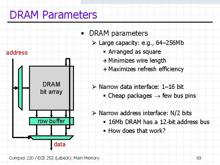
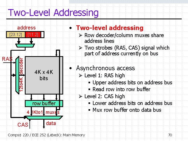
DRAM Parameters • DRAM parameters Ø Large capacity: e. g. , 64– 256 Mb § Arranged as square + Minimizes wire length + Maximizes refresh efficiency address DRAM bit array row buffer Ø Narrow data interface: 1– 16 bit § Cheap packages few bus pins Ø Narrow address interface: N/2 bits § 16 Mb DRAM has a 12 -bit address bus § How does that work? data Compsci 220 / ECE 252 (Lebeck): Main Memory 69

Two-Level Addressing • Two-level addressing address RAS Ø Row decoder/column muxes share address lines Ø Two strobes (RAS, CAS) signal which part of address currently on bus [11: 2] 12 to 4 K decoder [23: 12] 4 K x 4 K bits row buffer 4 1 Kto 1 muxes CAS • Asynchronous access Ø Level 1: RAS high § Upper address bits on address bus § Read row into row buffer Ø Level 2: CAS high § Lower address bits on address bus § Mux row buffer onto data bus data Compsci 220 / ECE 252 (Lebeck): Main Memory 70

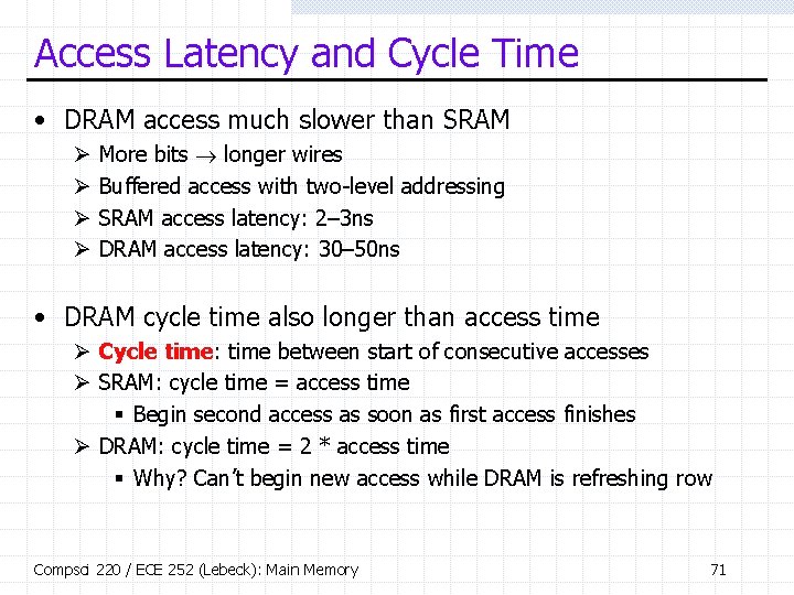
Access Latency and Cycle Time • DRAM access much slower than SRAM Ø Ø More bits longer wires Buffered access with two-level addressing SRAM access latency: 2– 3 ns DRAM access latency: 30– 50 ns • DRAM cycle time also longer than access time Ø Cycle time: time between start of consecutive accesses Ø SRAM: cycle time = access time § Begin second access as soon as first access finishes Ø DRAM: cycle time = 2 * access time § Why? Can’t begin new access while DRAM is refreshing row Compsci 220 / ECE 252 (Lebeck): Main Memory 71

DRAM Latency and Power Derivations • Same basic form as SRAM Ø Most of the equations are geometrically derived Ø Same structure for decoders, wordlines, muxes • Some differences Ø Somewhat different pre-charge/sensing scheme Ø Array access represents smaller part of total access Ø Arrays not multi-ported Compsci 220 / ECE 252 (Lebeck): Main Memory 72

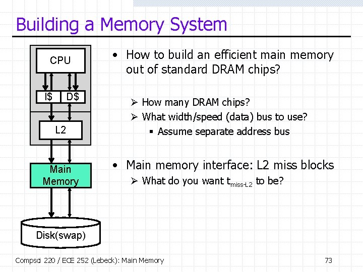
Building a Memory System CPU I$ D$ L 2 Main Memory • How to build an efficient main memory out of standard DRAM chips? Ø How many DRAM chips? Ø What width/speed (data) bus to use? § Assume separate address bus • Main memory interface: L 2 miss blocks Ø What do you want tmiss-L 2 to be? Disk(swap) Compsci 220 / ECE 252 (Lebeck): Main Memory 73

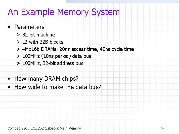
An Example Memory System • Parameters Ø Ø Ø 32 -bit machine L 2 with 32 B blocks 4 Mx 16 b DRAMs, 20 ns access time, 40 ns cycle time 100 MHz (10 ns period) data bus 100 MHz, 32 -bit address bus • How many DRAM chips? • How wide to make the data bus? Compsci 220 / ECE 252 (Lebeck): Main Memory 74

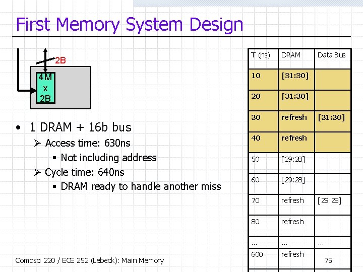
First Memory System Design 2 B 4 M x 2 B • 1 DRAM + 16 b bus Ø Access time: 630 ns § Not including address Ø Cycle time: 640 ns § DRAM ready to handle another miss Compsci 220 / ECE 252 (Lebeck): Main Memory T (ns) DRAM 10 [31: 30] 20 [31: 30] 30 refresh 40 refresh 50 [29: 28] 60 [29: 28] 70 refresh 80 refresh … … 600 refresh Data Bus [31: 30] [29: 28] … 75
![Second Memory System Design T ns DRAM 10 31 30 20 31 30 30 Second Memory System Design T (ns) DRAM 10 [31: 30] 20 [31: 30] 30](https://slidetodoc.com/presentation_image_h2/52e5da7c0a0b1360bec622b25ff30b8f/image-76.jpg)
Second Memory System Design T (ns) DRAM 10 [31: 30] 20 [31: 30] 30 refresh [31 H] Ø One DRAM chip, don’t need 16 b bus Ø Balanced system match bandwidths Ø DRAM: 2 B / 40 ns 4 b / 10 ns 40 refresh [31 L] 50 [29: 28] [30 H] 60 [29: 28] [30 L] Ø Access time: 660 ns (30 ns longer, 4%) Ø Cycle time: 640 ns (same) + Much cheaper 70 refresh [29 H] 80 refresh [29 L] … … … 600 [1: 0] 610 [1: 0] [2 H] 76 [2 L] 4 b 4 M x 2 B • 1 DRAM + 4 b bus Compsci 220 / ECE 252 (Lebeck): Main Memory Bus

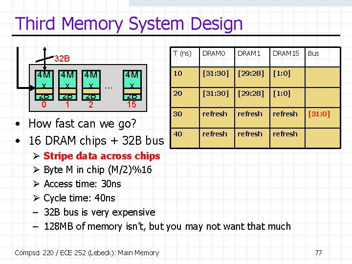
Third Memory System Design 32 B 4 M x 2 B 0 4 M x 2 B 1 4 M x … 2 B 2 4 M x 2 B 15 • How fast can we go? • 16 DRAM chips + 32 B bus Ø Ø – – T (ns) DRAM 0 DRAM 15 10 [31: 30] [29: 28] [1: 0] 20 [31: 30] [29: 28] [1: 0] 30 refresh 40 refresh Bus [31: 0] Stripe data across chips Byte M in chip (M/2)%16 Access time: 30 ns Cycle time: 40 ns 32 B bus is very expensive 128 MB of memory isn’t, but you may not want that much Compsci 220 / ECE 252 (Lebeck): Main Memory 77

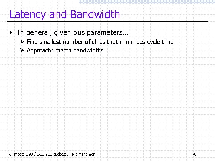
Latency and Bandwidth • In general, given bus parameters… Ø Find smallest number of chips that minimizes cycle time Ø Approach: match bandwidths Compsci 220 / ECE 252 (Lebeck): Main Memory 78

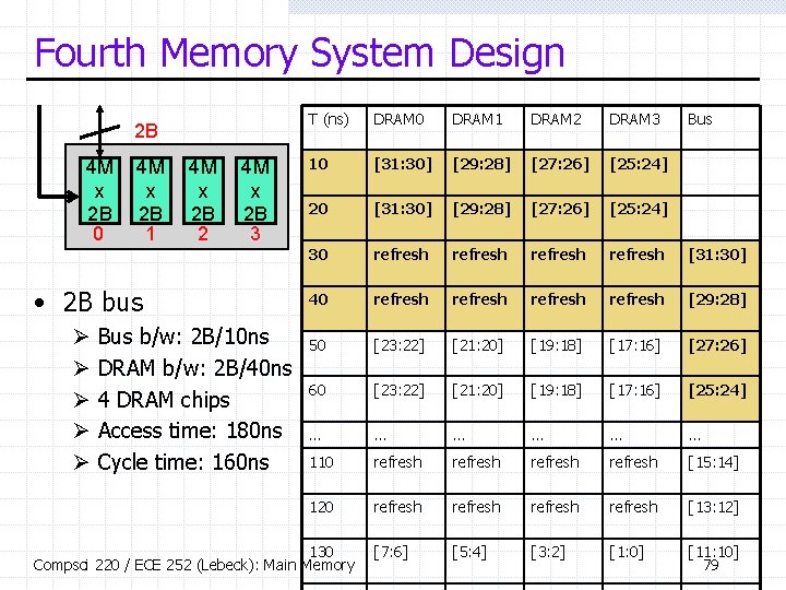
Fourth Memory System Design 2 B 4 M x 2 B 0 4 M x 2 B 1 4 M x 2 B 2 4 M x 2 B 3 • 2 B bus Ø Ø Ø Bus b/w: 2 B/10 ns DRAM b/w: 2 B/40 ns 4 DRAM chips Access time: 180 ns Cycle time: 160 ns T (ns) DRAM 0 DRAM 1 DRAM 2 DRAM 3 10 [31: 30] [29: 28] [27: 26] [25: 24] 20 [31: 30] [29: 28] [27: 26] [25: 24] 30 refresh [31: 30] 40 refresh [29: 28] 50 [23: 22] [21: 20] [19: 18] [17: 16] [27: 26] 60 [23: 22] [21: 20] [19: 18] [17: 16] [25: 24] … … … 110 refresh [15: 14] 120 refresh [13: 12] [7: 6] [5: 4] [3: 2] [1: 0] [11: 10] 79 130 Compsci 220 / ECE 252 (Lebeck): Main Memory Bus

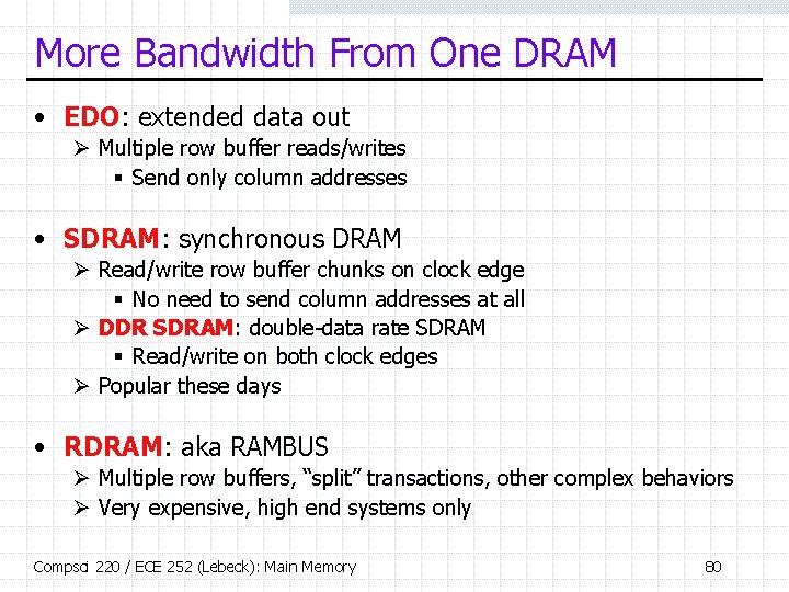
More Bandwidth From One DRAM • EDO: extended data out Ø Multiple row buffer reads/writes § Send only column addresses • SDRAM: synchronous DRAM Ø Read/write row buffer chunks on clock edge § No need to send column addresses at all Ø DDR SDRAM: double-data rate SDRAM § Read/write on both clock edges Ø Popular these days • RDRAM: aka RAMBUS Ø Multiple row buffers, “split” transactions, other complex behaviors Ø Very expensive, high end systems only Compsci 220 / ECE 252 (Lebeck): Main Memory 80

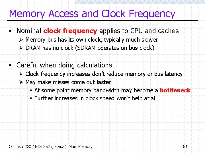
Memory Access and Clock Frequency • Nominal clock frequency applies to CPU and caches Ø Memory bus has its own clock, typically much slower Ø DRAM has no clock (SDRAM operates on bus clock) • Careful when doing calculations Ø Clock frequency increases don’t reduce memory or bus latency Ø May make misses come out faster § At some point memory bandwidth may become a bottleneck § Further increases in clock speed won’t help at all Compsci 220 / ECE 252 (Lebeck): Main Memory 81

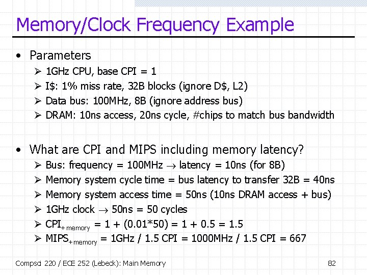
Memory/Clock Frequency Example • Parameters Ø Ø 1 GHz CPU, base CPI = 1 I$: 1% miss rate, 32 B blocks (ignore D$, L 2) Data bus: 100 MHz, 8 B (ignore address bus) DRAM: 10 ns access, 20 ns cycle, #chips to match bus bandwidth • What are CPI and MIPS including memory latency? Ø Ø Ø Bus: frequency = 100 MHz latency = 10 ns (for 8 B) Memory system cycle time = bus latency to transfer 32 B = 40 ns Memory system access time = 50 ns (10 ns DRAM access + bus) 1 GHz clock 50 ns = 50 cycles CPI+memory = 1 + (0. 01*50) = 1 + 0. 5 = 1. 5 MIPS+memory = 1 GHz / 1. 5 CPI = 1000 MHz / 1. 5 CPI = 667 Compsci 220 / ECE 252 (Lebeck): Main Memory 82

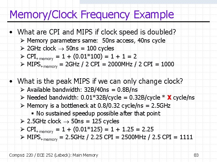
Memory/Clock Frequency Example • What are CPI and MIPS if clock speed is doubled? Ø Ø Memory parameters same: 50 ns access, 40 ns cycle 2 GHz clock 50 ns = 100 cycles CPI+memory = 1 + (0. 01*100) = 1 + 1 = 2 MIPS+memory = 2 GHz / 2 CPI = 2000 MHz / 2 CPI = 1000 • What is the peak MIPS if we can only change clock? Ø Available bandwidth: 32 B/40 ns = 0. 8 B/ns Ø Needed bandwidth: 0. 01*32 B/cycle = 0. 32 B/cycle * X cycle/ns Ø Memory is a bottleneck at 0. 8/0. 32 cycle/ns = 2. 5 GHz § No sustained speedup possible after that point Ø 2. 5 GHz clock 50 ns = 125 cycles Ø CPI+memory = 1 + (0. 01*125) = 1 + 1. 25 = 2. 25 Ø MIPS+memory = 2. 5 GHz / 2. 25 CPI = 2500 MHz / 2. 5 CPI = 1111 Compsci 220 / ECE 252 (Lebeck): Main Memory 83

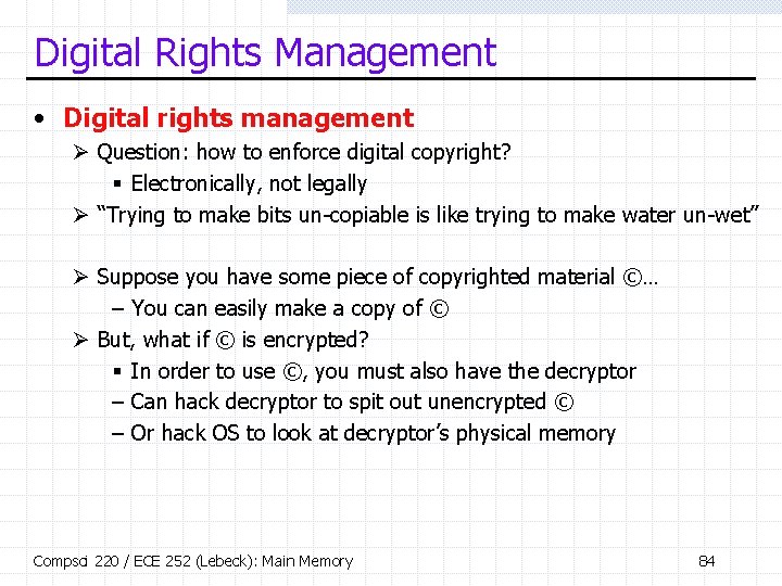
Digital Rights Management • Digital rights management Ø Question: how to enforce digital copyright? § Electronically, not legally Ø “Trying to make bits un-copiable is like trying to make water un-wet” Ø Suppose you have some piece of copyrighted material ©… – You can easily make a copy of © Ø But, what if © is encrypted? § In order to use ©, you must also have the decryptor – Can hack decryptor to spit out unencrypted © – Or hack OS to look at decryptor’s physical memory Compsci 220 / ECE 252 (Lebeck): Main Memory 84

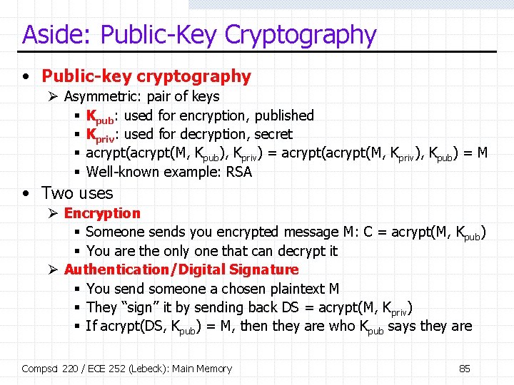
Aside: Public-Key Cryptography • Public-key cryptography Ø Asymmetric: pair of keys § Kpub: used for encryption, published § Kpriv: used for decryption, secret § acrypt(M, Kpub), Kpriv) = acrypt(M, Kpriv), Kpub) = M § Well-known example: RSA • Two uses Ø Encryption § Someone sends you encrypted message M: C = acrypt(M, Kpub) § You are the only one that can decrypt it Ø Authentication/Digital Signature § You send someone a chosen plaintext M § They “sign” it by sending back DS = acrypt(M, Kpriv) § If acrypt(DS, Kpub) = M, then they are who Kpub says they are Compsci 220 / ECE 252 (Lebeck): Main Memory 85

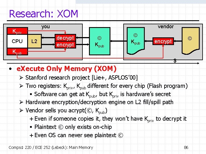
Research: XOM you Kpriv CPU L 2 vendor decrypt encrypt © Kpub © encrypt Kpub $ • e. Xecute Only Memory (XOM) Ø Stanford research project [Lie+, ASPLOS’ 00] Ø Two registers: Kpriv, Kpub different for every chip (Flash program) § Software can get at Kpub, but Kpriv is hardware’s secret Ø Hardware encryption/decryption engine on L 2 fill/spill path Ø Vendor sells you acrypt(©, Kpub) + Even if someone copies it, they won’t have Kpriv to decrypt it § Plaintext © only exists on-chip + Even OS can never see plaintext © Compsci 220 / ECE 252 (Lebeck): Main Memory 86

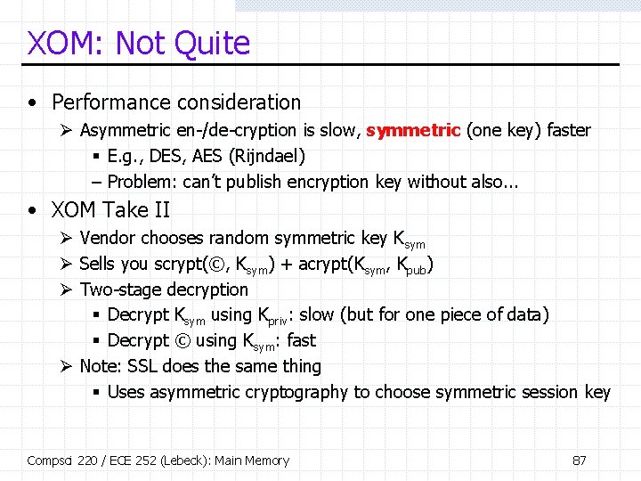
XOM: Not Quite • Performance consideration Ø Asymmetric en-/de-cryption is slow, symmetric (one key) faster § E. g. , DES, AES (Rijndael) – Problem: can’t publish encryption key without also. . . • XOM Take II Ø Vendor chooses random symmetric key Ksym Ø Sells you scrypt(©, Ksym) + acrypt(Ksym, Kpub) Ø Two-stage decryption § Decrypt Ksym using Kpriv: slow (but for one piece of data) § Decrypt © using Ksym: fast Ø Note: SSL does the same thing § Uses asymmetric cryptography to choose symmetric session key Compsci 220 / ECE 252 (Lebeck): Main Memory 87

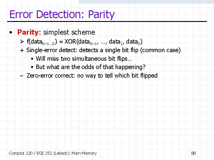
Error Detection: Parity • Parity: simplest scheme Ø f(data. N– 1… 0) = XOR(data. N– 1, …, data 1, data 0) + Single-error detect: detects a single bit flip (common case) § Will miss two simultaneous bit flips… § But what are the odds of that happening? – Zero-error correct: no way to tell which bit flipped Compsci 220 / ECE 252 (Lebeck): Main Memory 88

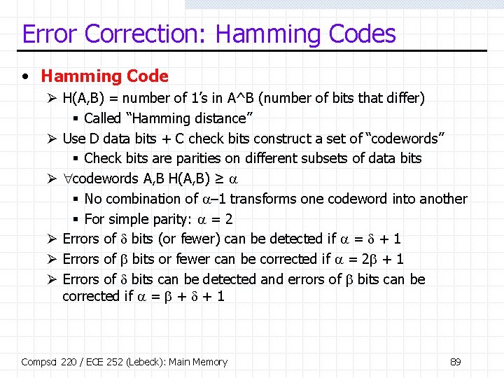
Error Correction: Hamming Codes • Hamming Code Ø H(A, B) = number of 1’s in A^B (number of bits that differ) § Called “Hamming distance” Ø Use D data bits + C check bits construct a set of “codewords” § Check bits are parities on different subsets of data bits Ø codewords A, B H(A, B) ≥ § No combination of – 1 transforms one codeword into another § For simple parity: = 2 Ø Errors of bits (or fewer) can be detected if = + 1 Ø Errors of bits or fewer can be corrected if = 2 + 1 Ø Errors of bits can be detected and errors of bits can be corrected if = + + 1 Compsci 220 / ECE 252 (Lebeck): Main Memory 89

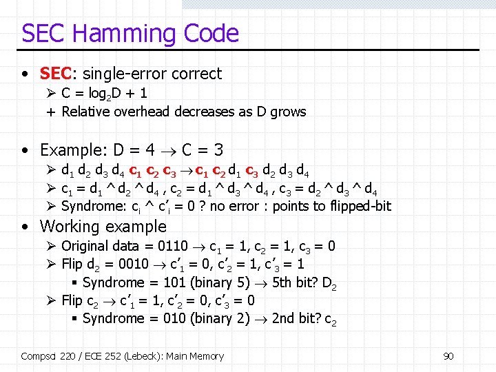
SEC Hamming Code • SEC: single-error correct Ø C = log 2 D + 1 + Relative overhead decreases as D grows • Example: D = 4 C = 3 Ø d 1 d 2 d 3 d 4 c 1 c 2 c 3 c 1 c 2 d 1 c 3 d 2 d 3 d 4 Ø c 1 = d 1 ^ d 2 ^ d 4 , c 2 = d 1 ^ d 3 ^ d 4 , c 3 = d 2 ^ d 3 ^ d 4 Ø Syndrome: ci ^ c’i = 0 ? no error : points to flipped-bit • Working example Ø Original data = 0110 c 1 = 1, c 2 = 1, c 3 = 0 Ø Flip d 2 = 0010 c’ 1 = 0, c’ 2 = 1, c’ 3 = 1 § Syndrome = 101 (binary 5) 5 th bit? D 2 Ø Flip c 2 c’ 1 = 1, c’ 2 = 0, c’ 3 = 0 § Syndrome = 010 (binary 2) 2 nd bit? c 2 Compsci 220 / ECE 252 (Lebeck): Main Memory 90

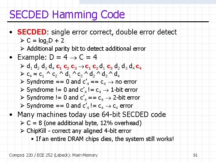
SECDED Hamming Code • SECDED: single error correct, double error detect Ø C = log 2 D + 2 Ø Additional parity bit to detect additional error • Example: D = 4 C = 4 Ø Ø Ø d 1 d 2 d 3 d 4 c 1 c 2 c 3 c 1 c 2 d 1 c 3 d 2 d 3 d 4 c 4 = c 1 ^ c 2 ^ d 1 ^ c 3 ^ d 2 ^ d 3 ^ d 4 Syndrome == 0 and c’ 4 == c 4 no error Syndrome != 0 and c’ 4 != c 4 1 -bit error Syndrome != 0 and c’ 4 == c 4 2 -bit error Syndrome == 0 and c’ 4 != c 4 error • Many machines today use 64 -bit SECDED code Ø C = 8 (one additional byte, 12% overhead) Ø Chip. Kill - correct any aligned 4 -bit error § If an entire DRAM chips dies, the system still works! Compsci 220 / ECE 252 (Lebeck): Main Memory 91