Digital Logic Circuits Part 1 Computer Architecture Fall
- Slides: 22

Digital Logic Circuits (Part 1) Computer Architecture (Fall 2006)

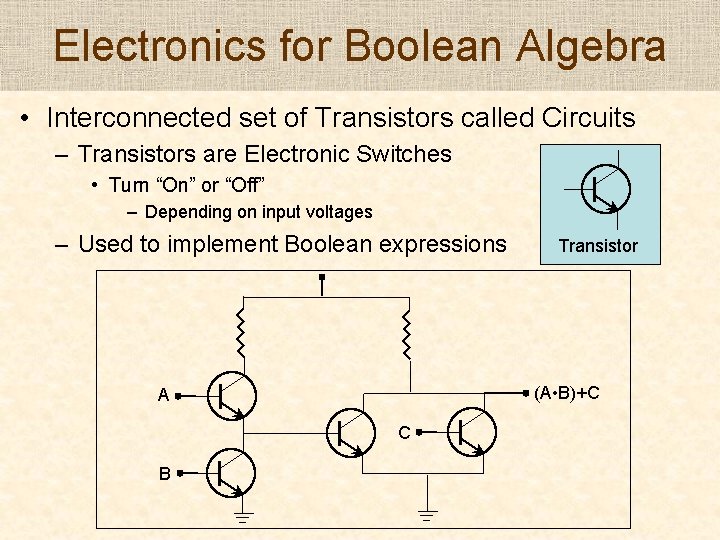
Electronics for Boolean Algebra • Interconnected set of Transistors called Circuits – Transistors are Electronic Switches • Turn “On” or “Off” – Depending on input voltages – Used to implement Boolean expressions (A • B)+C A C B Transistor

Logic Gates • Developing large circuits is complex – Drawing many transistors is cumbersome – Makes the circuit diagram unwieldy • Hard to illustrate and comprehend • Solution: Logic Gates – Abstract notation for common logic circuits • Functionally similar to set of transistors – Simpler to develop and use

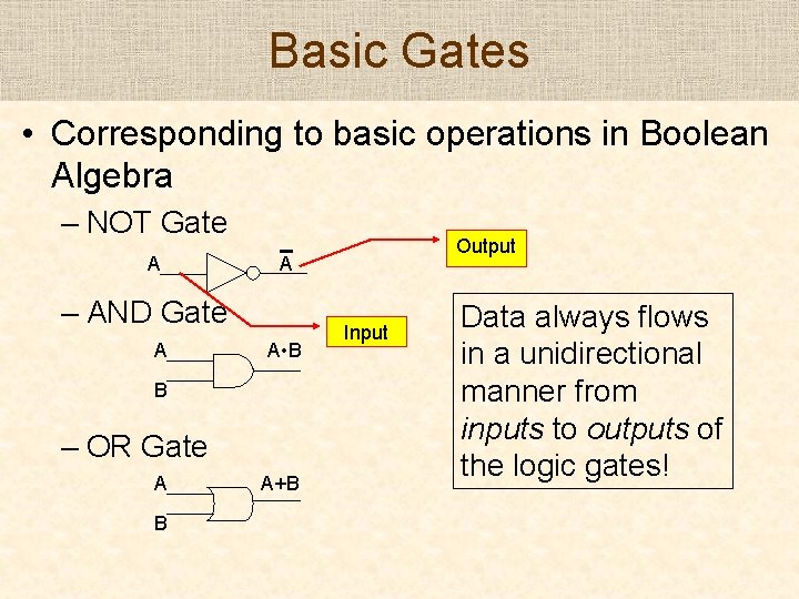
Basic Gates • Corresponding to basic operations in Boolean Algebra – NOT Gate A A – AND Gate A A • B B – OR Gate A B Output A+B Input Data always flows in a unidirectional manner from inputs to outputs of the logic gates!

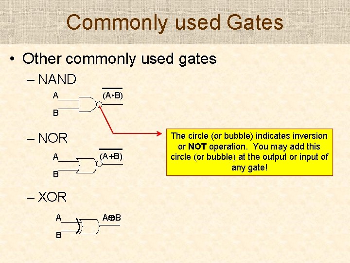
Commonly used Gates • Other commonly used gates – NAND A (A • B) B – NOR A (A+B) B – XOR A B The circle (or bubble) indicates inversion or NOT operation. You may add this circle (or bubble) at the output or input of any gate!

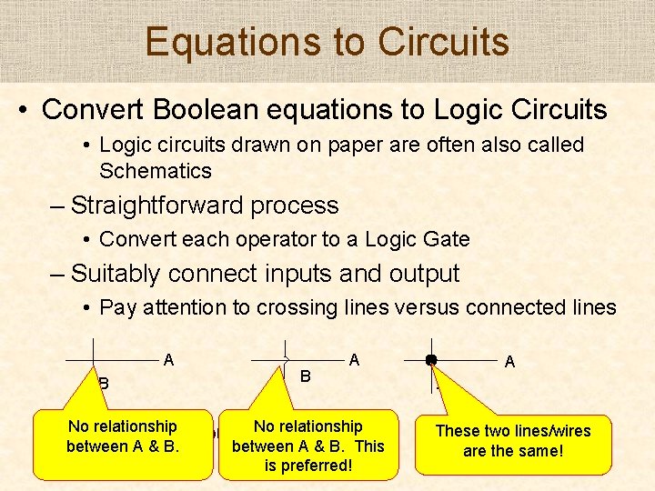
Equations to Circuits • Convert Boolean equations to Logic Circuits • Logic circuits drawn on paper are often also called Schematics – Straightforward process • Convert each operator to a Logic Gate – Suitably connect inputs and output • Pay attention to crossing lines versus connected lines A B No • relationship Label all between A & B. B A No relationship inputs and outputs between A & B. This is preferred! A A These two lines/wires are the same!

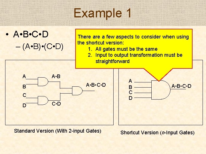
Example 1 • A • B • C • D – (A • B) • (C • D) A There a few aspects to consider when using the shortcut version: 1. All gates must be the same 2. Input to output transformation must be straightforward A • B • C • D B C D A • B • C • D Standard Version (With 2 -input Gates) Shortcut Version (n-Input Gates)

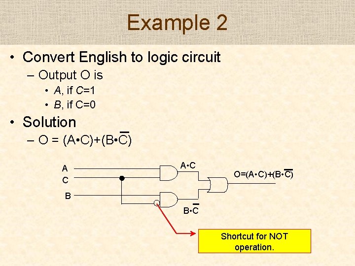
Example 2 • Convert English to logic circuit – Output O is • A, if C=1 • B, if C=0 • Solution – O = (A • C)+(B • C) A C A • C O=(A • C)+(B • C) B B • C Shortcut for NOT operation.

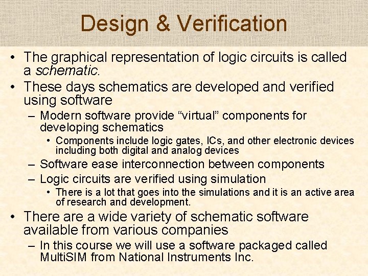
Design & Verification • The graphical representation of logic circuits is called a schematic. • These days schematics are developed and verified using software – Modern software provide “virtual” components for developing schematics • Components include logic gates, ICs, and other electronic devices including both digital and analog devices – Software ease interconnection between components – Logic circuits are verified using simulation • There is a lot that goes into the simulations and it is an active area of research and development. • There a wide variety of schematic software available from various companies – In this course we will use a software packaged called Multi. SIM from National Instruments Inc.

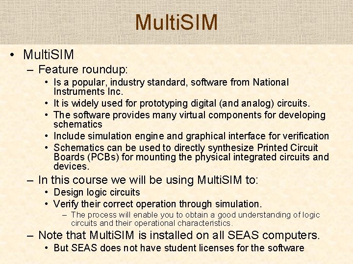
Multi. SIM • Multi. SIM – Feature roundup: • Is a popular, industry standard, software from National Instruments Inc. • It is widely used for prototyping digital (and analog) circuits. • The software provides many virtual components for developing schematics • Include simulation engine and graphical interface for verification • Schematics can be used to directly synthesize Printed Circuit Boards (PCBs) for mounting the physical integrated circuits and devices. – In this course we will be using Multi. SIM to: • Design logic circuits • Verify their correct operation through simulation. – The process will enable you to obtain a good understanding of logic circuits and their operational characteristics. – Note that Multi. SIM is installed on all SEAS computers. • But SEAS does not have student licenses for the software

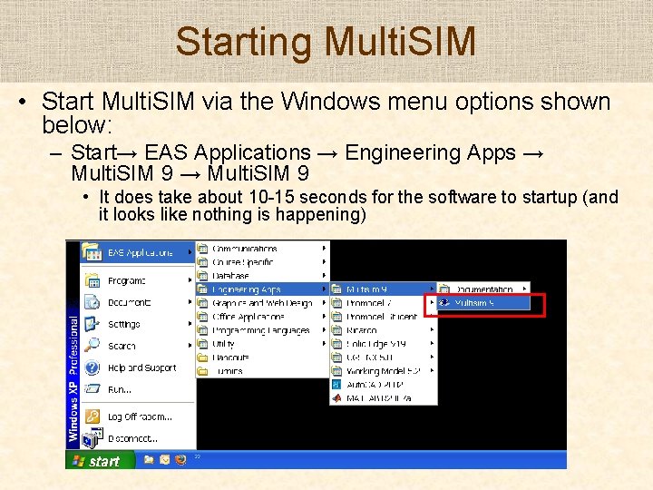
Starting Multi. SIM • Start Multi. SIM via the Windows menu options shown below: – Start→ EAS Applications → Engineering Apps → Multi. SIM 9 • It does take about 10 -15 seconds for the software to startup (and it looks like nothing is happening)

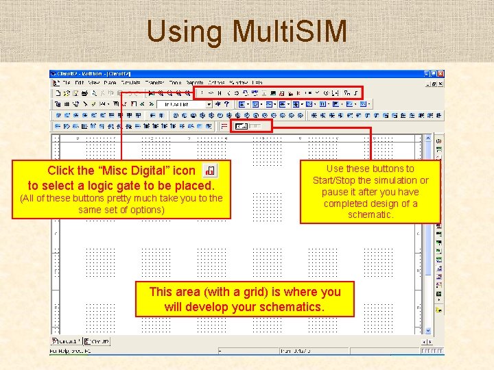
Using Multi. SIM Click the “Misc Digital” icon to select a logic gate to be placed. (All of these buttons pretty much take you to the same set of options) Use these buttons to Start/Stop the simulation or pause it after you have completed design of a schematic. This area (with a grid) is where you will develop your schematics.

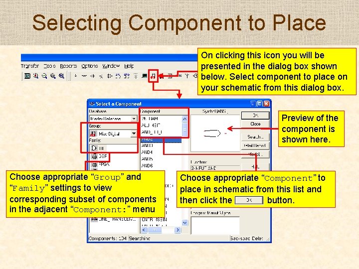
Selecting Component to Place On clicking this icon you will be presented in the dialog box shown below. Select component to place on your schematic from this dialog box. Preview of the component is shown here. Choose appropriate “Group” and “Family” settings to view corresponding subset of components in the adjacent “Component: ” menu Choose appropriate “Component” to place in schematic from this list and then click the button.

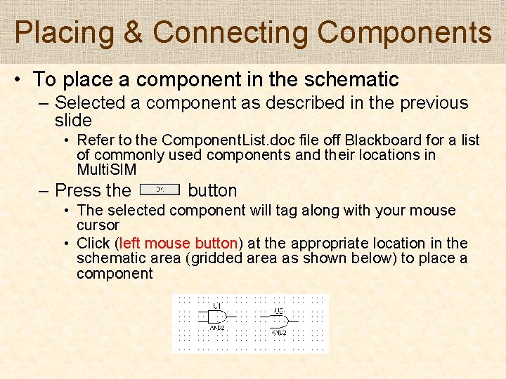
Placing & Connecting Components • To place a component in the schematic – Selected a component as described in the previous slide • Refer to the Component. List. doc file off Blackboard for a list of commonly used components and their locations in Multi. SIM – Press the button • The selected component will tag along with your mouse cursor • Click (left mouse button) at the appropriate location in the schematic area (gridded area as shown below) to place a component

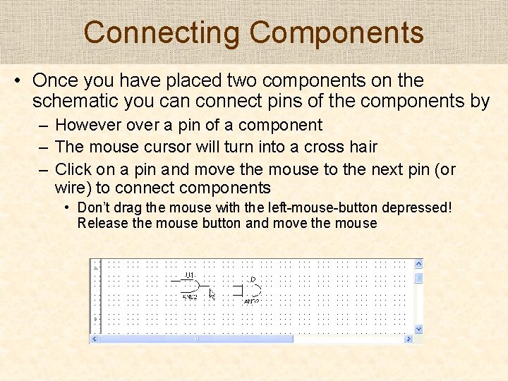
Connecting Components • Once you have placed two components on the schematic you can connect pins of the components by – However over a pin of a component – The mouse cursor will turn into a cross hair – Click on a pin and move the mouse to the next pin (or wire) to connect components • Don’t drag the mouse with the left-mouse-button depressed! Release the mouse button and move the mouse

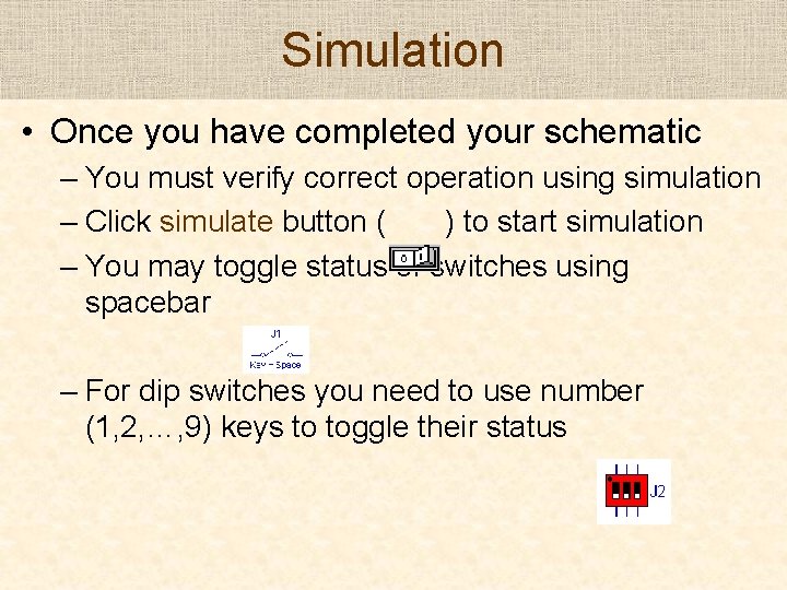
Simulation • Once you have completed your schematic – You must verify correct operation using simulation – Click simulate button ( ) to start simulation – You may toggle status of switches using spacebar – For dip switches you need to use number (1, 2, …, 9) keys to toggle their status

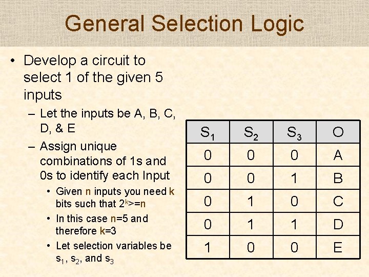
General Selection Logic • Develop a circuit to select 1 of the given 5 inputs – Let the inputs be A, B, C, D, & E – Assign unique combinations of 1 s and 0 s to identify each Input • Given n inputs you need k bits such that 2 k>=n • In this case n=5 and therefore k=3 • Let selection variables be s 1, s 2, and s 3 S 1 S 2 S 3 O 0 0 0 A 0 0 1 B 0 1 0 C 0 1 1 D 1 0 0 E

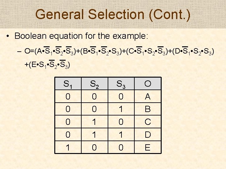
General Selection (Cont. ) • Boolean equation for the example: – O=(A • S 1 • S 2 • S 3)+(B • S 1 • S 2 • S 3)+(C • S 1 • S 2 • S 3)+(D • S 1 • S 2 • S 3) +(E • S 1 • S 2 • S 3) S 1 0 0 1 S 2 0 0 1 1 0 S 3 0 1 0 O A B C D E

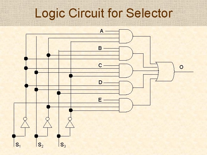
Logic Circuit for Selector A B C D E S 1 S 2 S 3 O

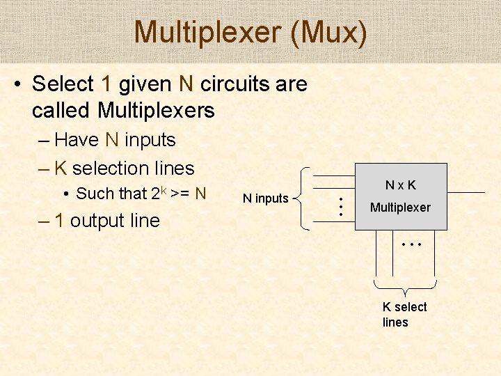
Multiplexer (Mux) • Select 1 given N circuits are called Multiplexers – Have N inputs – K selection lines – 1 output line >= N N inputs Nx. K • • • • Such that 2 k Multiplexer • • • K select lines

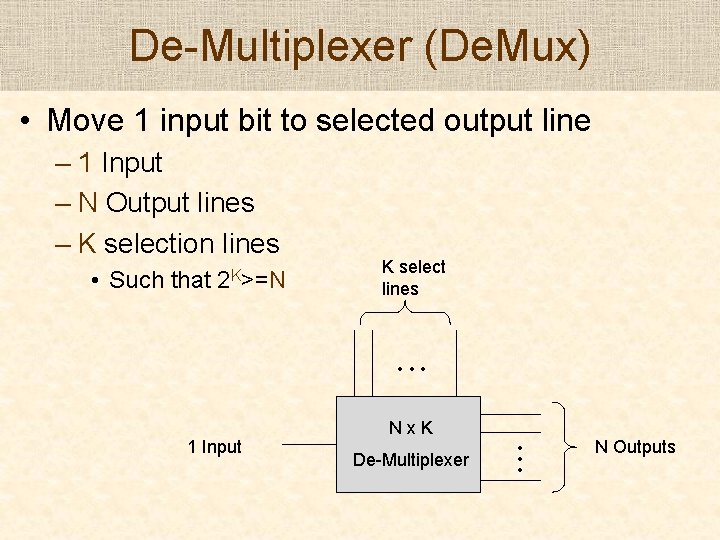
De-Multiplexer (De. Mux) • Move 1 input bit to selected output line – 1 Input – N Output lines – K selection lines • Such that 2 K>=N K select lines • • • De-Multiplexer • • • 1 Input Nx. K N Outputs

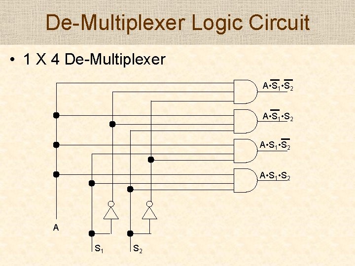
De-Multiplexer Logic Circuit • 1 X 4 De-Multiplexer A • S 1 • S 2 A S 1 S 2