CSCE 212 Introduction to Computer Architecture Instructor Jason
- Slides: 31
CSCE 212 Introduction to Computer Architecture Instructor: Jason D. Bakos
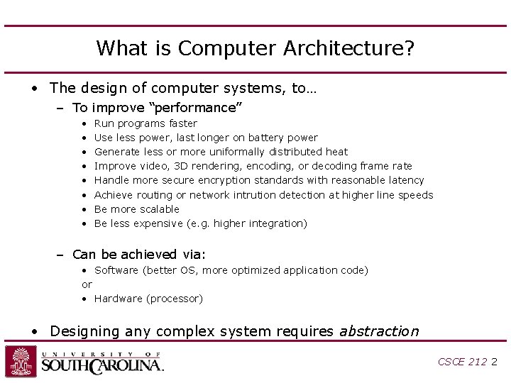
What is Computer Architecture? • The design of computer systems, to… – To improve “performance” • • Run programs faster Use less power, last longer on battery power Generate less or more uniformally distributed heat Improve video, 3 D rendering, encoding, or decoding frame rate Handle more secure encryption standards with reasonable latency Achieve routing or network intrution detection at higher line speeds Be more scalable Be less expensive (e. g. higher integration) – Can be achieved via: • Software (better OS, more optimized application code) or • Hardware (processor) • Designing any complex system requires abstraction CSCE 212 2
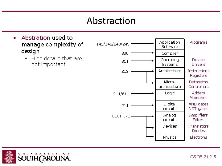
Abstraction • Abstration used to manage complexity of design – Hide details that are not important 145/146/240/245 Application Software Programs 330 Compiler 311 Operating Systems Device Drivers 212 Architecture Instructions Registers Microarchitecture Datapaths Controllers Logic Adders Memories Digital circuits AND gates NOT gates Analog circuits Amplifiers Filters Devices Transistors Diodes Physics Electrons 211/611 211 ELCT 371 CSCE 212 3
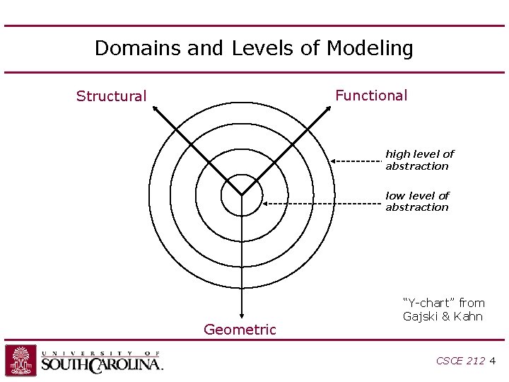
Domains and Levels of Modeling Functional Structural high level of abstraction low level of abstraction Geometric “Y-chart” from Gajski & Kahn CSCE 212 4
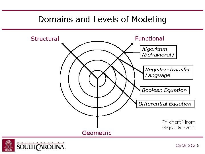
Domains and Levels of Modeling Functional Structural Algorithm (behavioral) Register-Transfer Language Boolean Equation Differential Equation Geometric “Y-chart” from Gajski & Kahn CSCE 212 5
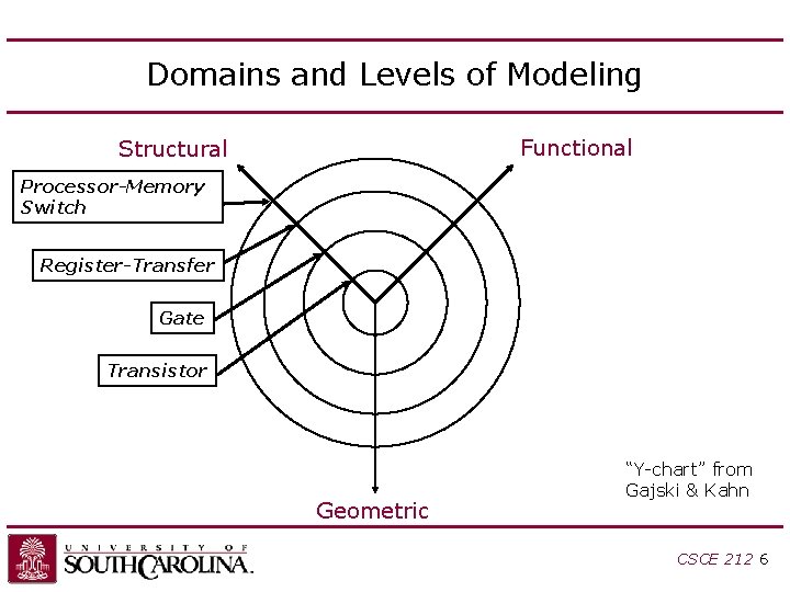
Domains and Levels of Modeling Functional Structural Processor-Memory Switch Register-Transfer Gate Transistor Geometric “Y-chart” from Gajski & Kahn CSCE 212 6
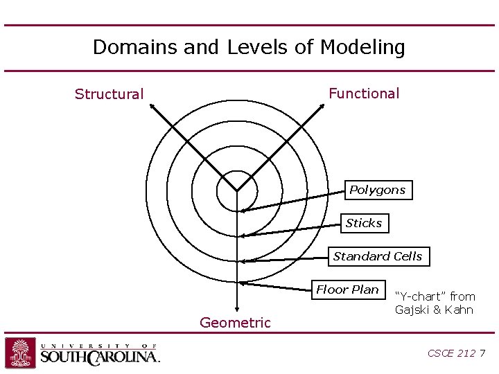
Domains and Levels of Modeling Functional Structural Polygons Sticks Standard Cells Floor Plan Geometric “Y-chart” from Gajski & Kahn CSCE 212 7
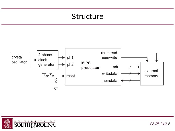
Structure CSCE 212 8
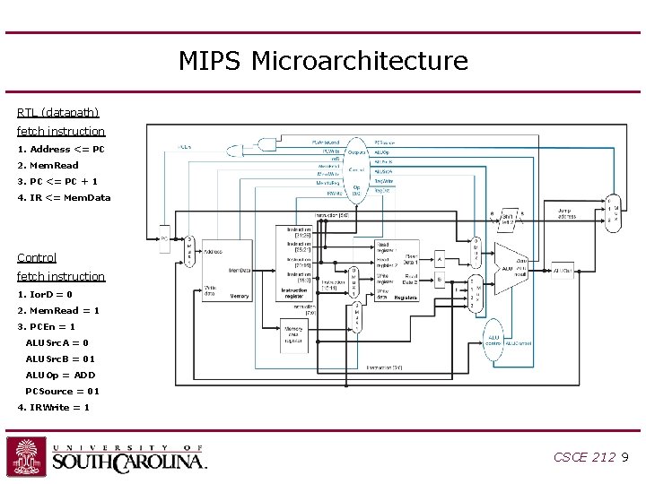
MIPS Microarchitecture RTL (datapath) fetch instruction 1. Address <= PC 2. Mem. Read 3. PC <= PC + 1 4. IR <= Mem. Data Control fetch instruction 1. Ior. D = 0 2. Mem. Read = 1 3. PCEn = 1 ALUSrc. A = 0 ALUSrc. B = 01 ALUOp = ADD PCSource = 01 4. IRWrite = 1 CSCE 212 9
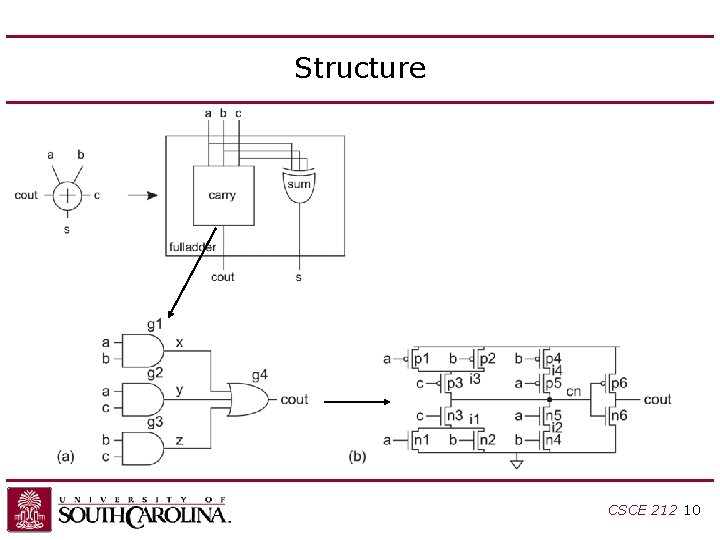
Structure CSCE 212 10
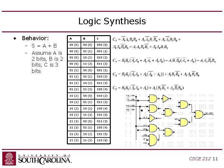
Logic Synthesis • Behavior: – S=A+B – Assume A is 2 bits, B is 2 bits, C is 3 bits A B C 00 (0) 000 (0) 01 (1) 00 (0) 10 (2) 00 (0) 11 (3) 01 (1) 00 (0) 001 (1) 010 (2) 01 (1) 10 (2) 011 (3) 01 (1) 11 (3) 100 (4) 10 (2) 00 (0) 010 (2) 01 (1) 011 (3) 10 (2) 100 (4) 10 (2) 11 (3) 101 (5) 11 (3) 00 (0) 011 (3) 01 (1) 100 (4) 11 (3) 10 (2) 101 (5) 11 (3) 110 (6) CSCE 212 11
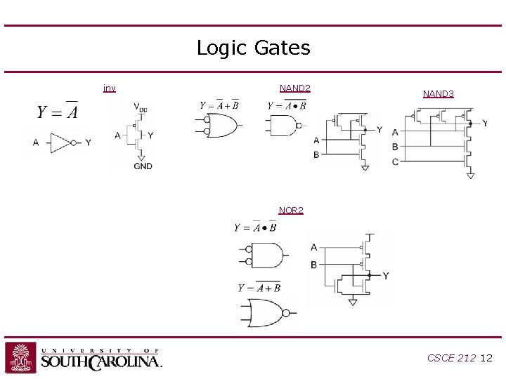
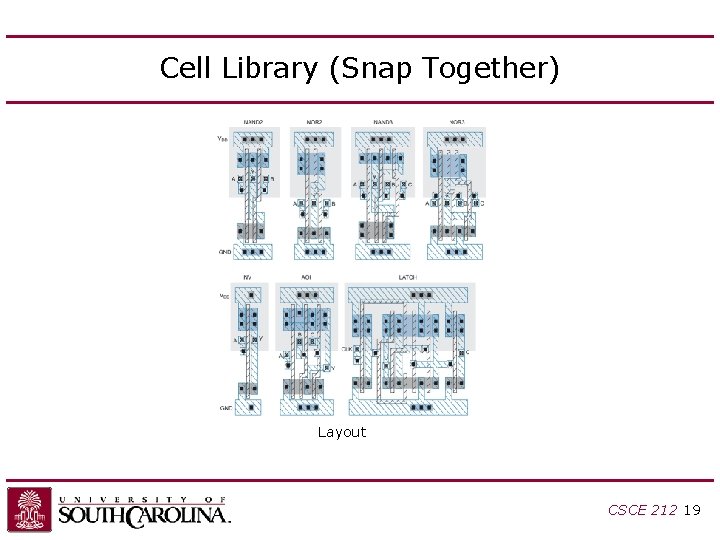
Logic Gates inv NAND 2 NAND 3 NOR 2 CSCE 212 12
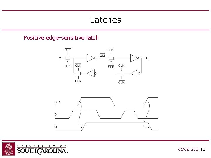
Latches Positive edge-sensitive latch CSCE 212 13
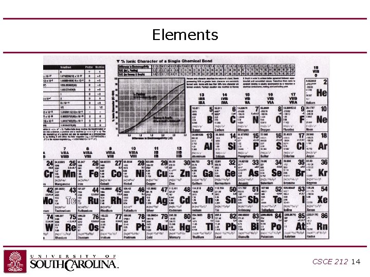
Elements CSCE 212 14
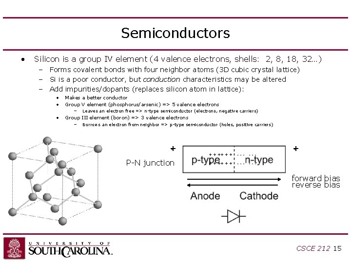
Semiconductors • Silicon is a group IV element (4 valence electrons, shells: 2, 8, 18, 32…) – Forms covalent bonds with four neighbor atoms (3 D cubic crystal lattice) – Si is a poor conductor, but conduction characteristics may be altered – Add impurities/dopants (replaces silicon atom in lattice): • • Makes a better conductor Group V element (phosphorus/arsenic) => 5 valence electrons – • Leaves an electron free => n-type semiconductor (electrons, negative carriers) Group III element (boron) => 3 valence electrons – Borrows an electron from neighbor => p-type semiconductor (holes, positive carriers) +P-N junction + + ++ + + --- --- +forward bias reverse bias CSCE 212 15
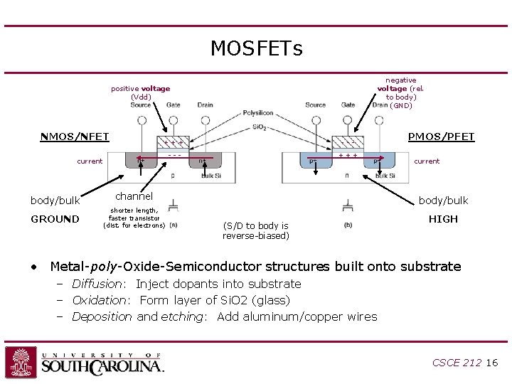
MOSFETs negative voltage (rel. to body) (GND) positive voltage (Vdd) NMOS/NFET current body/bulk GROUND --- +++ channel shorter length, faster transistor (dist. for electrons) PMOS/PFET current body/bulk (S/D to body is reverse-biased) HIGH • Metal-poly-Oxide-Semiconductor structures built onto substrate – Diffusion: Inject dopants into substrate – Oxidation: Form layer of Si. O 2 (glass) – Deposition and etching: Add aluminum/copper wires CSCE 212 16
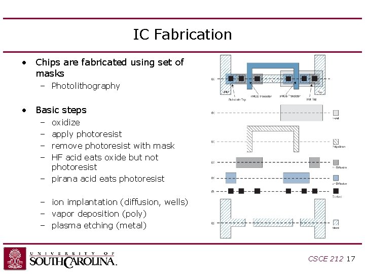
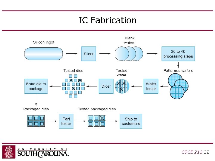
IC Fabrication • Chips are fabricated using set of masks – Photolithography • Basic steps – – oxidize apply photoresist remove photoresist with mask HF acid eats oxide but not photoresist – pirana acid eats photoresist – ion implantation (diffusion, wells) – vapor deposition (poly) – plasma etching (metal) CSCE 212 17
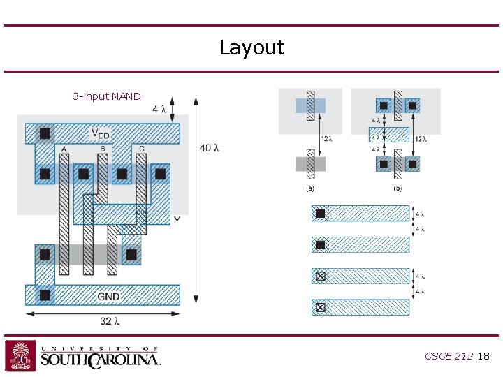
Layout 3 -input NAND CSCE 212 18
Cell Library (Snap Together) Layout CSCE 212 19
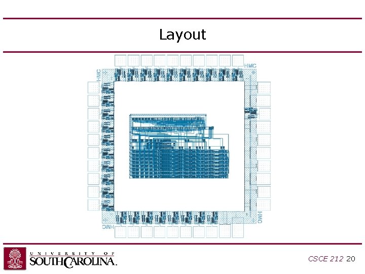
Layout CSCE 212 20
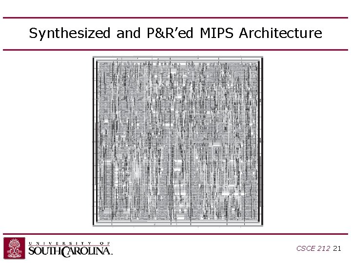
Synthesized and P&R’ed MIPS Architecture CSCE 212 21
IC Fabrication CSCE 212 22
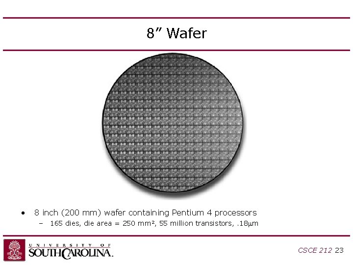
8” Wafer • 8 inch (200 mm) wafer containing Pentium 4 processors – 165 dies, die area = 250 mm 2, 55 million transistors, . 18 mm CSCE 212 23
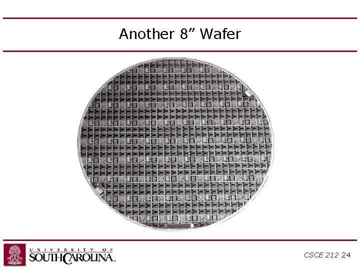
Another 8” Wafer CSCE 212 24
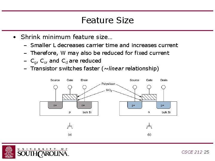
Feature Size • Shrink minimum feature size… – – Smaller L decreases carrier time and increases current Therefore, W may also be reduced for fixed current Cg, Cs, and Cd are reduced Transistor switches faster (~linear relationship) CSCE 212 25
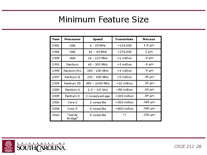
Minimum Feature Size Year Processor Speed Transistors Process 1982 i 286 6 - 25 MHz ~134, 000 1. 5 mm 1986 i 386 16 – 40 MHz ~270, 000 1 mm 1989 i 486 16 - 133 MHz ~1 million . 8 mm 1993 Pentium 60 - 300 MHz ~3 million . 6 mm 1995 Pentium Pro 150 - 200 MHz ~4 million . 5 mm 1997 Pentium II 233 - 450 MHz ~5 million . 35 mm 1999 Pentium III 450 – 1400 MHz ~10 million . 25 mm 2000 Pentium 4 1. 3 – 3. 8 GHz ~50 million . 18 mm 2005 Pentium D 2 cores/package ~200 million . 09 mm 2006 Core 2 2 cores/die ~300 million . 065 mm 2008 Core i 7 4 cores/die ~800 million . 040 mm 2010 “Sandy Bridge” 8 cores/die ? ? . 032 mm CSCE 212 26
Clock Speed • Clock speed is affected by: – Fabrication technology – Architecture: how much work performed in a single cycle • Execution time = – instructions per program * cycles per instruction * seconds per cycle • Now we must add to the product: – (number of program threads / number of processor cores) CSCE 212 27
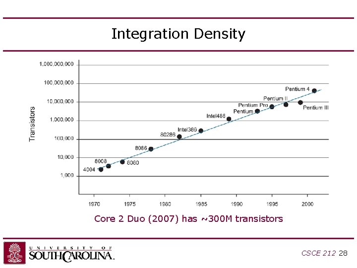
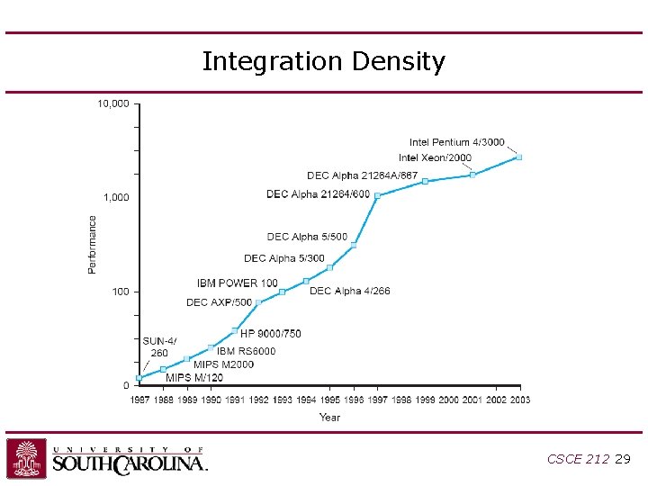
Integration Density Core 2 Duo (2007) has ~300 M transistors CSCE 212 28
Integration Density CSCE 212 29
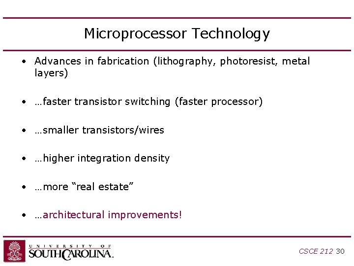
Microprocessor Technology • Advances in fabrication (lithography, photoresist, metal layers) • …faster transistor switching (faster processor) • …smaller transistors/wires • …higher integration density • …more “real estate” • …architectural improvements! CSCE 212 30
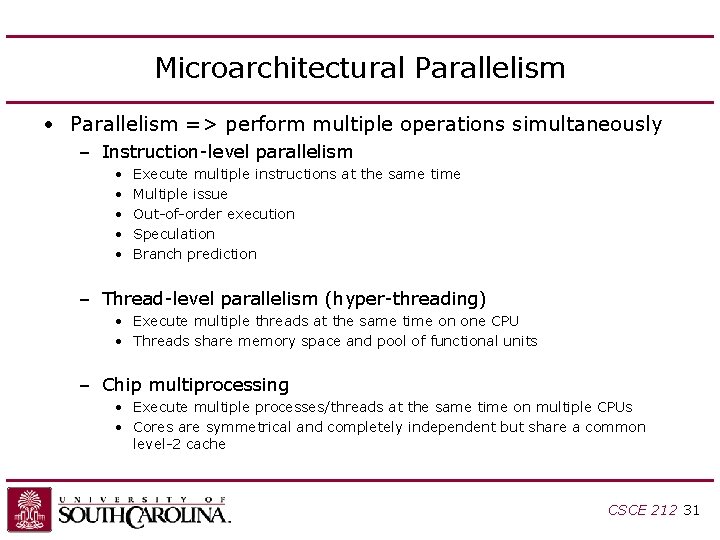
Microarchitectural Parallelism • Parallelism => perform multiple operations simultaneously – Instruction-level parallelism • • • Execute multiple instructions at the same time Multiple issue Out-of-order execution Speculation Branch prediction – Thread-level parallelism (hyper-threading) • Execute multiple threads at the same time on one CPU • Threads share memory space and pool of functional units – Chip multiprocessing • Execute multiple processes/threads at the same time on multiple CPUs • Cores are symmetrical and completely independent but share a common level-2 cache CSCE 212 31