College of Computer and Information Sciences Department of
- Slides: 36

College of Computer and Information Sciences Department of Computer Science CSC 220: Computer Organization Unit 8 Registers and RTL

Unit 8: Registers and RTL Overview • Registers • Parallel in Parallel out Registers • Shift Registers • Bus Construction • Register Transfer Language • Micro operations Chapter-6 M. Morris Mano, Charles R. Kime and Tom Martin, Logic and Computer Design Fundamentals, Global (5 th) Edition, Pearson Education Limited, 2016. ISBN: 9781292096124

3 Dr Mohamed A Berbar

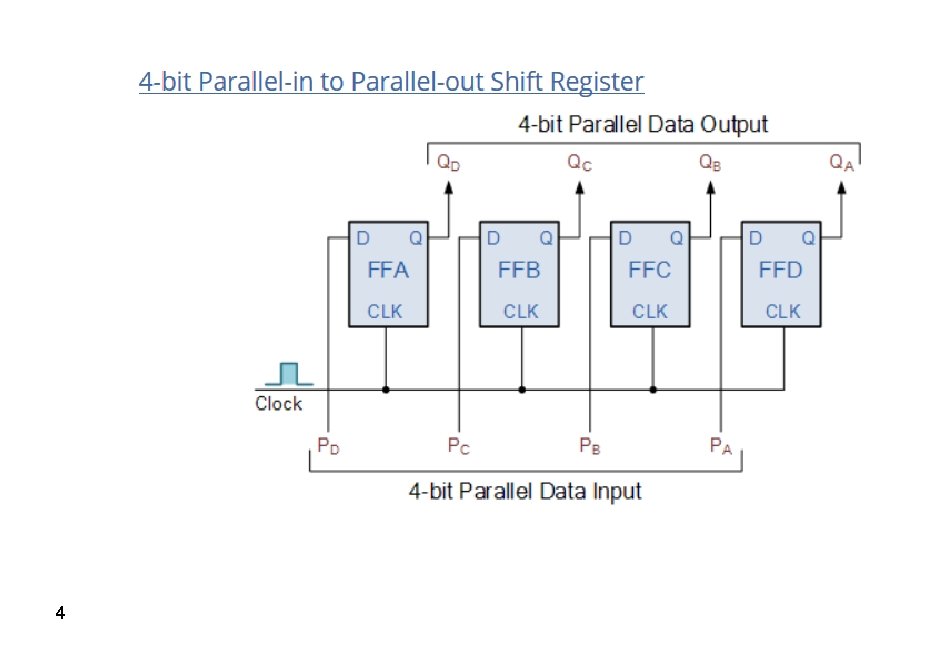
4

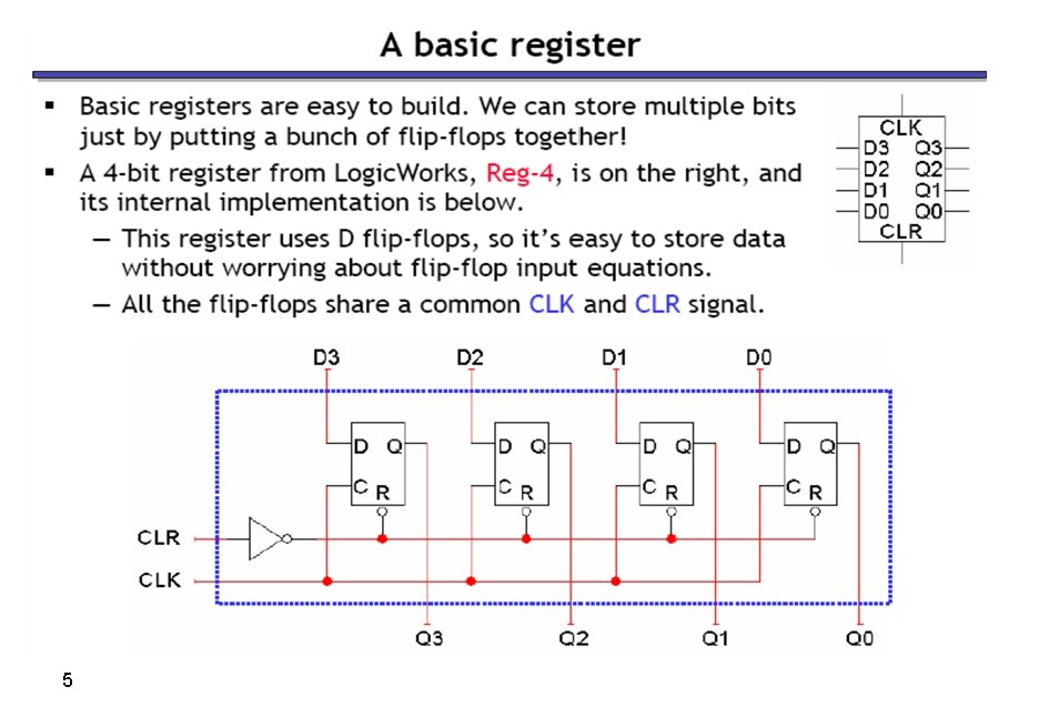
5

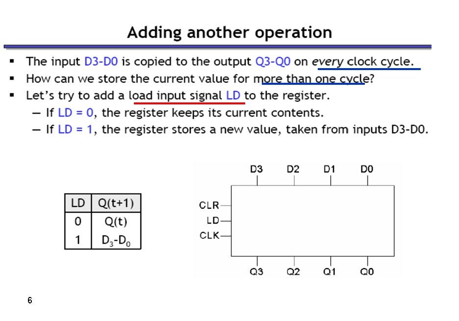
6

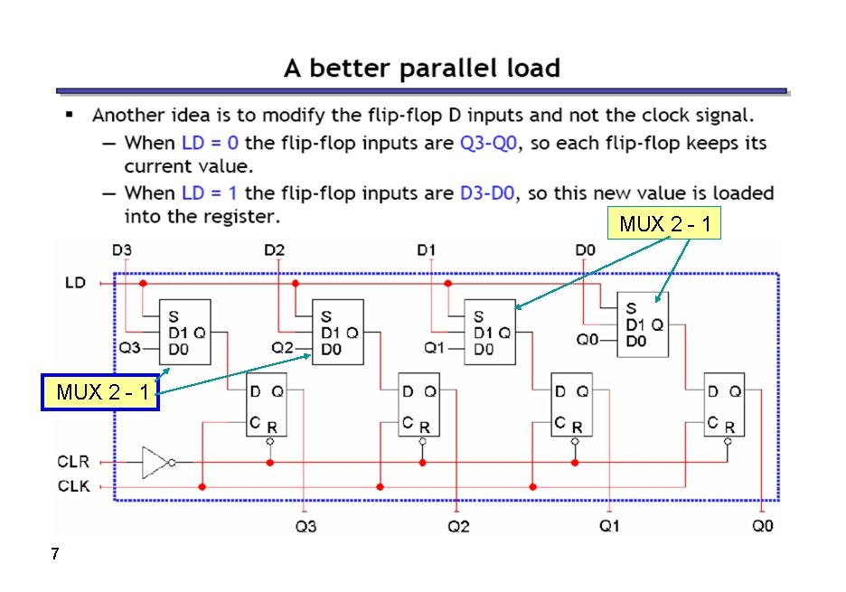
MUX 2 - 1 7

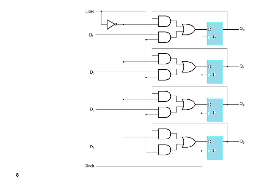
8

9

10

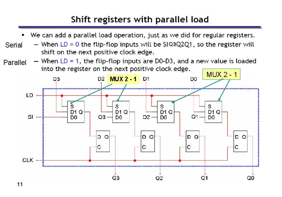
Serial Parallel MUX 2 - 1 11 MUX 2 - 1

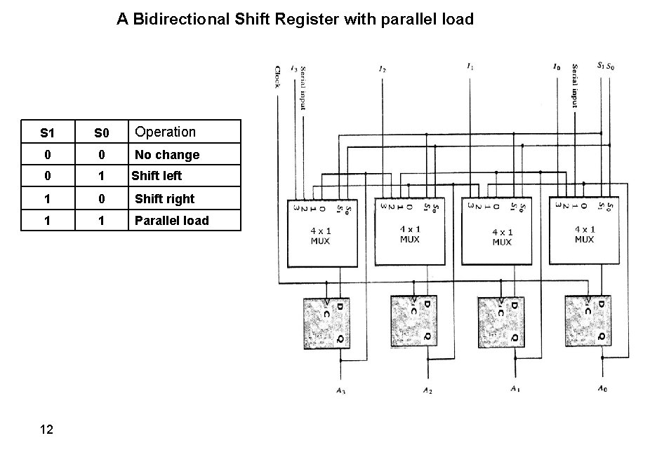
A Bidirectional Shift Register with parallel load S 1 S 0 Operation 0 0 No change 0 1 Shift left 1 0 Shift right 1 1 Parallel load 12

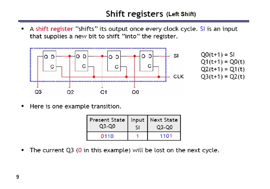
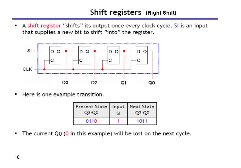
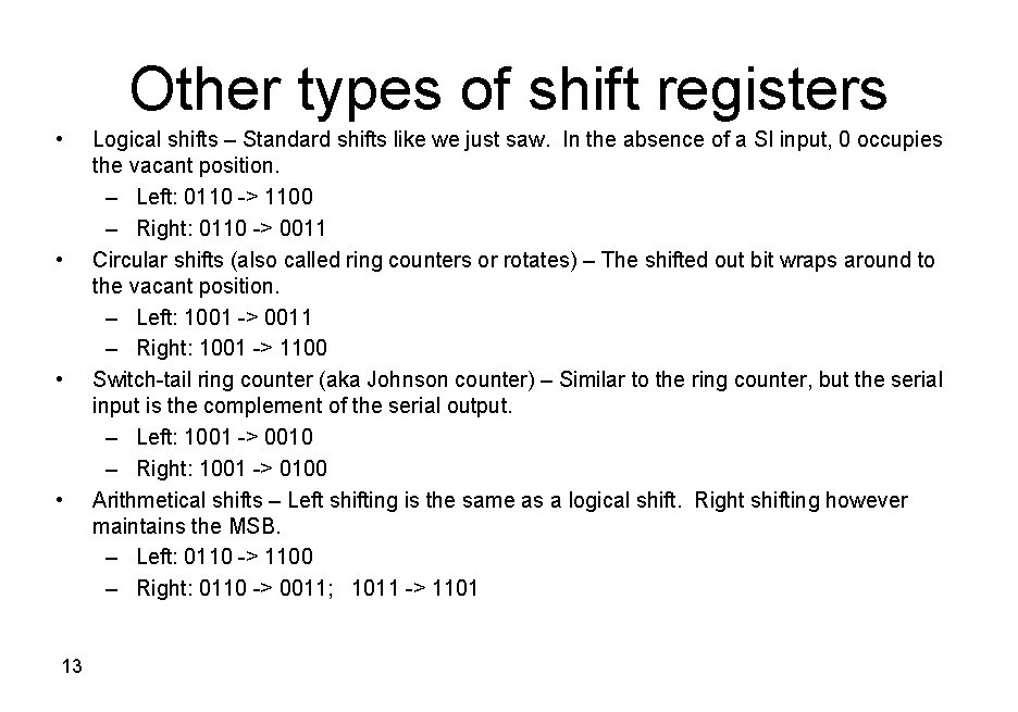
Other types of shift registers • • 13 Logical shifts – Standard shifts like we just saw. In the absence of a SI input, 0 occupies the vacant position. – Left: 0110 -> 1100 – Right: 0110 -> 0011 Circular shifts (also called ring counters or rotates) – The shifted out bit wraps around to the vacant position. – Left: 1001 -> 0011 – Right: 1001 -> 1100 Switch-tail ring counter (aka Johnson counter) – Similar to the ring counter, but the serial input is the complement of the serial output. – Left: 1001 -> 0010 – Right: 1001 -> 0100 Arithmetical shifts – Left shifting is the same as a logical shift. Right shifting however maintains the MSB. – Left: 0110 -> 1100 – Right: 0110 -> 0011; 1011 -> 1101

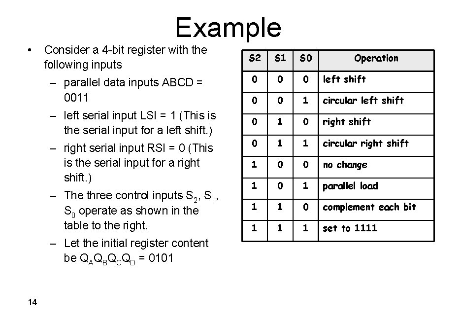
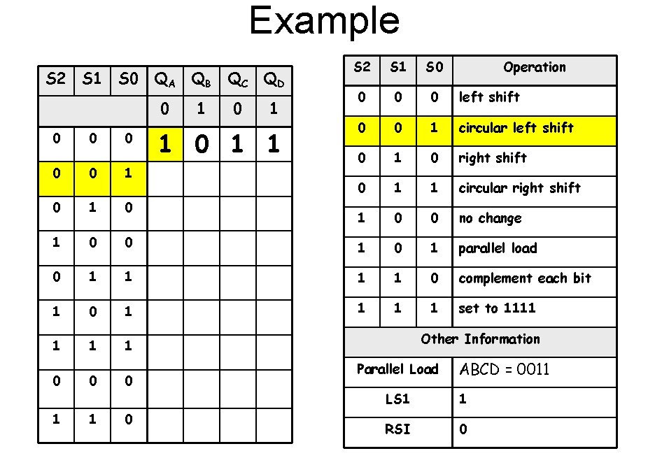
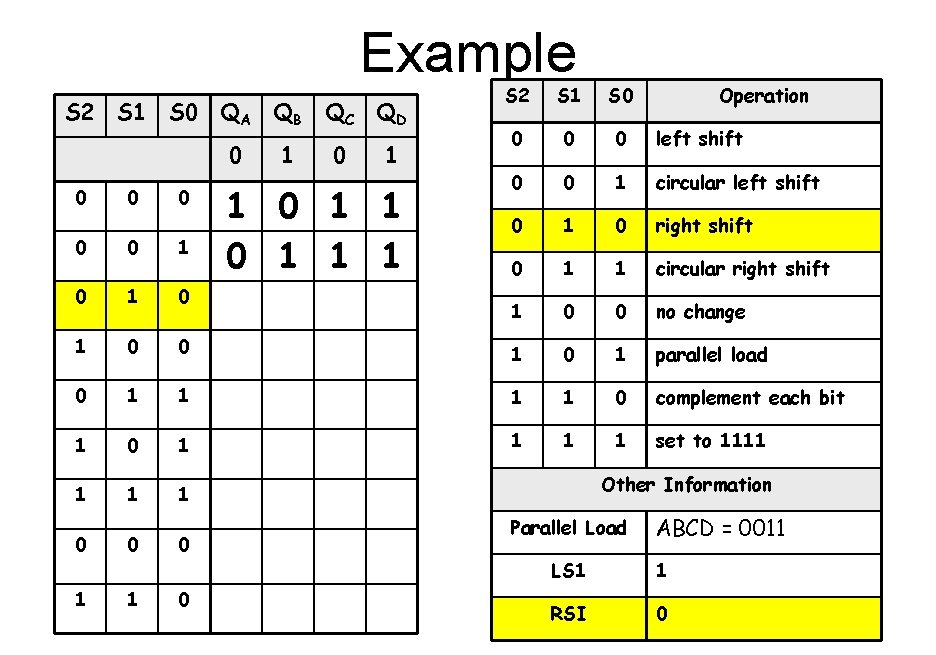
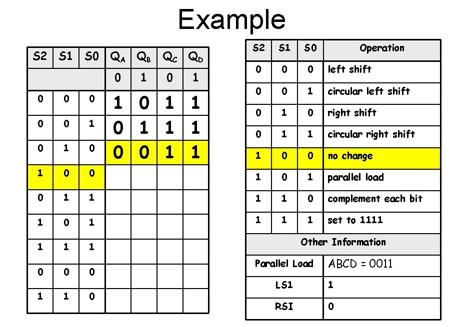
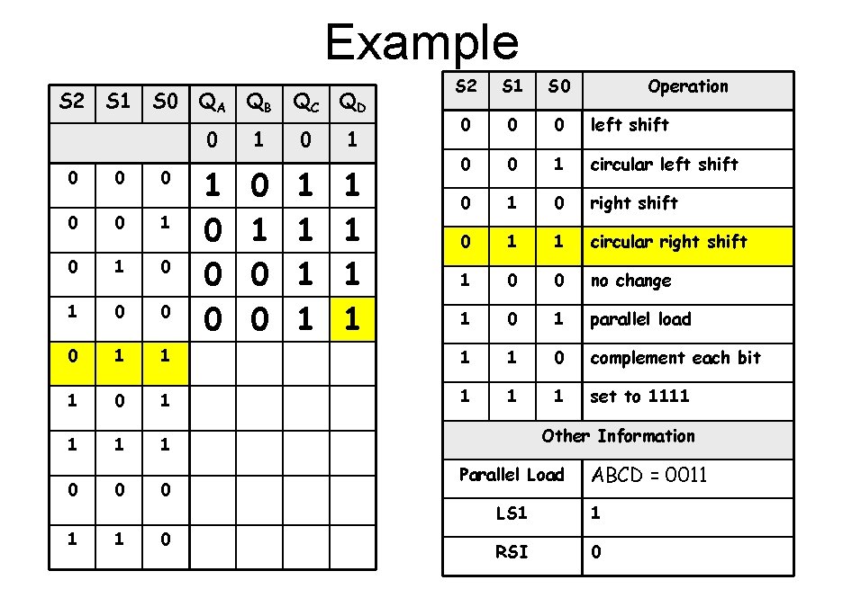
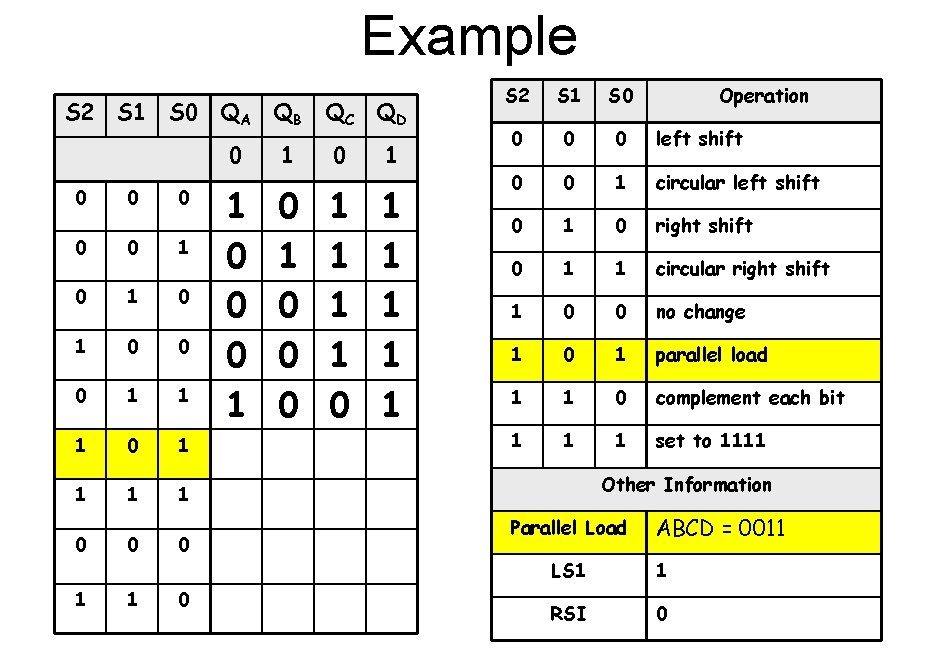
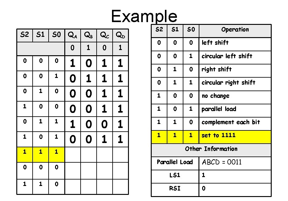
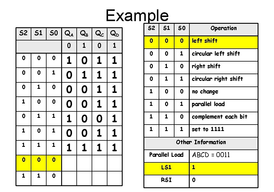
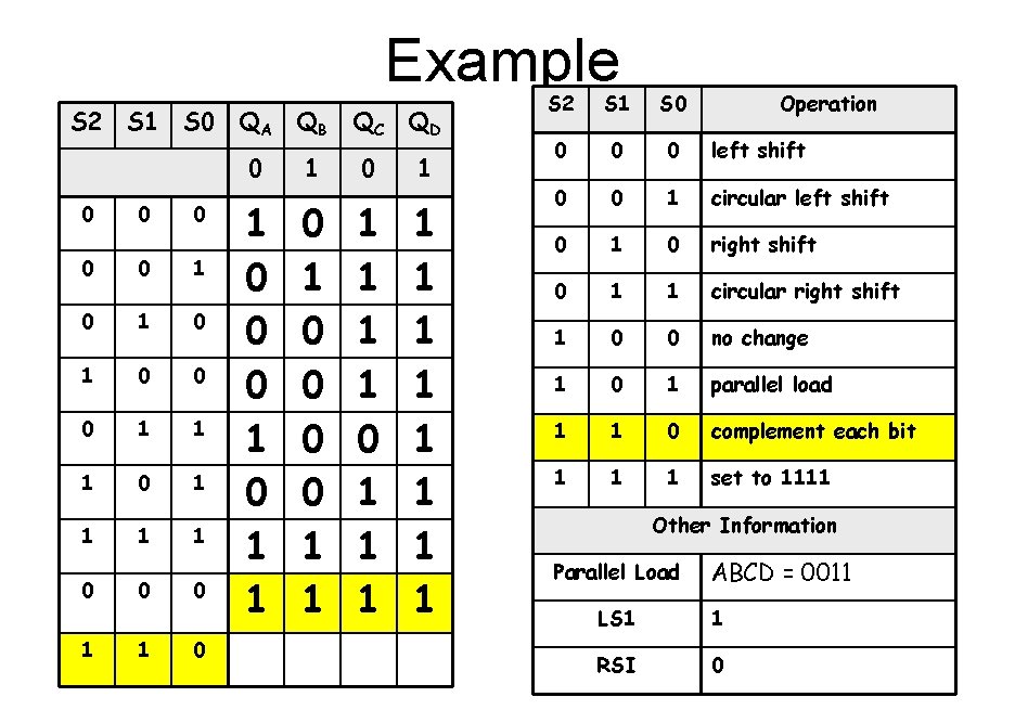
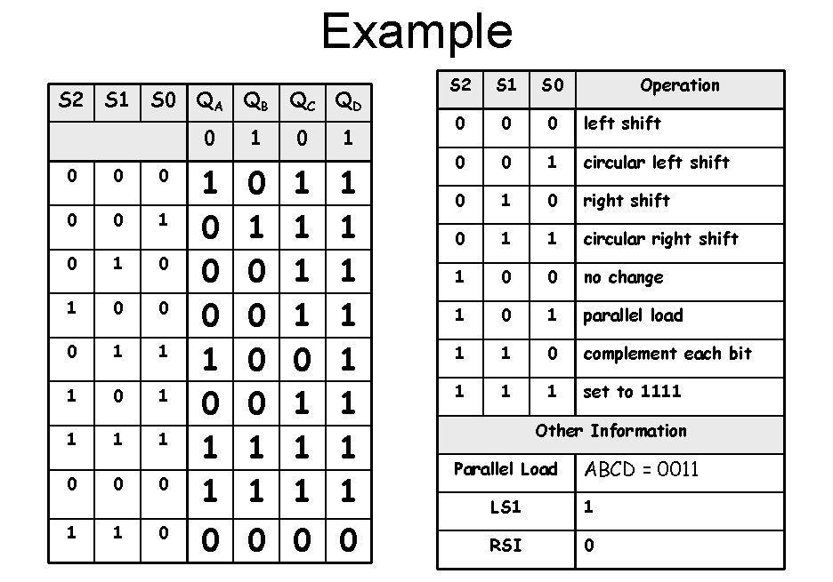
Example • Consider a 4 -bit register with the following inputs S 2 S 1 S 0 0 left shift 0 0 1 circular left shift – left serial input LSI = 1 (This is the serial input for a left shift. ) 0 1 0 right shift – right serial input RSI = 0 (This is the serial input for a right shift. ) 0 1 1 circular right shift 1 0 0 no change 1 0 1 parallel load 1 1 0 complement each bit 1 1 1 set to 1111 – parallel data inputs ABCD = 0011 – The three control inputs S 2, S 1, S 0 operate as shown in the table to the right. – Let the initial register content be QAQBQCQD = 0101 14 Operation

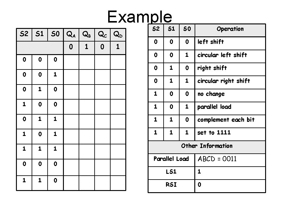
Example S 2 0 S 1 0 S 0 0 QA QB QC QD 0 1 S 2 S 1 S 0 Operation 0 0 0 left shift 0 0 1 circular left shift 0 1 0 right shift 0 1 1 circular right shift 1 0 0 no change 0 0 1 0 1 0 1 parallel load 0 1 1 0 complement each bit 1 0 1 1 set to 1111 1 0 0 0 1 1 0 15 Other Information Parallel Load ABCD = 0011 LS 1 1 RSI 0

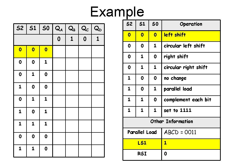
Example S 2 0 S 1 0 S 0 0 QA QB QC QD 0 1 S 2 S 1 S 0 Operation 0 0 0 left shift 0 0 1 circular left shift 0 1 0 right shift 0 1 1 circular right shift 1 0 0 no change 0 0 1 0 1 0 1 parallel load 0 1 1 0 complement each bit 1 0 1 1 set to 1111 1 0 0 0 1 1 0 16 Other Information Parallel Load ABCD = 0011 LS 1 1 RSI 0

Example S 2 0 S 1 0 S 0 0 QA QB QC QD 0 1 1 S 2 S 1 S 0 Operation 0 0 0 left shift 0 0 1 circular left shift 0 1 0 right shift 0 1 1 circular right shift 1 0 0 no change 0 0 1 0 1 0 1 parallel load 0 1 1 0 complement each bit 1 0 1 1 set to 1111 1 0 0 0 1 1 0 17 Other Information Parallel Load ABCD = 0011 LS 1 1 RSI 0

Example S 2 0 S 1 0 S 0 0 QA QB QC QD 0 1 1 1 S 2 S 1 S 0 Operation 0 0 0 left shift 0 0 1 circular left shift 0 1 0 right shift 0 1 1 circular right shift 1 0 0 no change 0 0 1 0 1 0 1 parallel load 0 1 1 0 complement each bit 1 0 1 1 set to 1111 1 0 0 0 1 1 0 18 Other Information Parallel Load ABCD = 0011 LS 1 1 RSI 0

Example S 2 0 S 1 0 S 0 0 QA QB QC QD 0 1 1 1 0 0 1 1 S 2 S 1 S 0 Operation 0 0 0 left shift 0 0 1 circular left shift 0 1 0 right shift 0 1 1 circular right shift 1 0 0 no change 0 0 1 0 1 0 1 parallel load 0 1 1 0 complement each bit 1 0 1 1 set to 1111 1 0 0 0 1 1 0 19 Other Information Parallel Load ABCD = 0011 LS 1 1 RSI 0

Example S 2 0 S 1 0 S 0 0 QA QB QC QD 0 1 1 0 0 1 1 1 1 S 2 S 1 S 0 Operation 0 0 0 left shift 0 0 1 circular left shift 0 1 0 right shift 0 1 1 circular right shift 1 0 0 no change 1 0 1 parallel load 0 0 1 0 1 0 0 0 1 1 0 complement each bit 1 0 1 1 set to 1111 1 0 0 0 1 1 0 20 Other Information Parallel Load ABCD = 0011 LS 1 1 RSI 0

Example S 2 0 S 1 0 S 0 0 1 0 1 0 0 0 1 1 1 1 0 0 0 1 1 0 21 QA QB QC QD 0 1 1 0 0 0 1 1 1 1 1 S 2 S 1 S 0 Operation 0 0 0 left shift 0 0 1 circular left shift 0 1 0 right shift 0 1 1 circular right shift 1 0 0 no change 1 0 1 parallel load 1 1 0 complement each bit 1 1 1 set to 1111 Other Information Parallel Load ABCD = 0011 LS 1 1 RSI 0

Example S 2 0 S 1 0 S 0 0 1 0 1 0 0 0 1 1 1 1 0 0 0 1 1 0 22 QA QB QC QD 0 1 1 0 0 0 1 1 0 1 1 1 1 S 2 S 1 S 0 Operation 0 0 0 left shift 0 0 1 circular left shift 0 1 0 right shift 0 1 1 circular right shift 1 0 0 no change 1 0 1 parallel load 1 1 0 complement each bit 1 1 1 set to 1111 Other Information Parallel Load ABCD = 0011 LS 1 1 RSI 0

Example S 2 0 S 1 0 S 0 0 1 0 1 0 0 0 1 1 1 1 0 0 0 1 1 0 23 QA QB QC QD 0 1 1 0 0 0 1 0 1 0 0 1 1 1 1 1 S 2 S 1 S 0 Operation 0 0 0 left shift 0 0 1 circular left shift 0 1 0 right shift 0 1 1 circular right shift 1 0 0 no change 1 0 1 parallel load 1 1 0 complement each bit 1 1 1 set to 1111 Other Information Parallel Load ABCD = 0011 LS 1 1 RSI 0

Example S 2 0 S 1 0 S 0 0 1 0 1 0 0 0 1 1 1 1 0 0 0 1 1 0 24 QA QB QC QD 0 1 1 0 0 0 0 1 1 1 1 1 S 2 S 1 S 0 Operation 0 0 0 left shift 0 0 1 circular left shift 0 1 0 right shift 0 1 1 circular right shift 1 0 0 no change 1 0 1 parallel load 1 1 0 complement each bit 1 1 1 set to 1111 Other Information Parallel Load ABCD = 0011 LS 1 1 RSI 0

Example S 2 0 S 1 0 S 0 0 1 0 1 0 0 0 1 1 1 1 0 0 0 1 1 0 25 QA QB QC QD 0 1 1 0 0 0 0 1 1 1 1 1 0 0 S 2 S 1 S 0 Operation 0 0 0 left shift 0 0 1 circular left shift 0 1 0 right shift 0 1 1 circular right shift 1 0 0 no change 1 0 1 parallel load 1 1 0 complement each bit 1 1 1 set to 1111 Other Information Parallel Load ABCD = 0011 LS 1 1 RSI 0

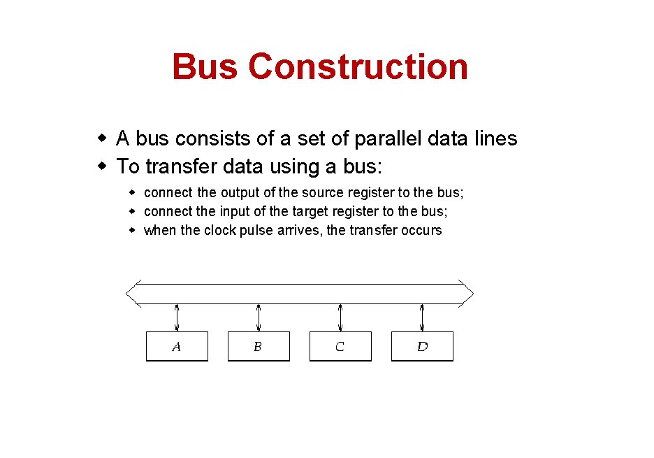
Bus Construction w A bus consists of a set of parallel data lines w To transfer data using a bus: w connect the output of the source register to the bus; w connect the input of the target register to the bus; w when the clock pulse arrives, the transfer occurs

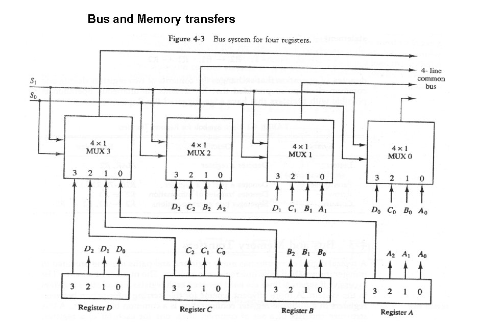
Bus and Memory transfers 27

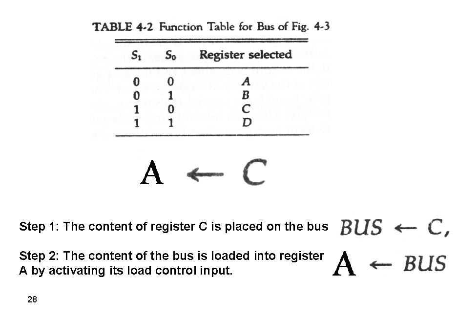
Step 1: The content of register C is placed on the bus Step 2: The content of the bus is loaded into register A by activating its load control input. 28

Question A digital computer has a common bus system for 16 registers of 32 bit each. The bus is constructed with multiplexers. – How many selection inputs are there is each multiplexer? – What size of multiplexers is needed? – How many multiplexers are there in the bus? 29

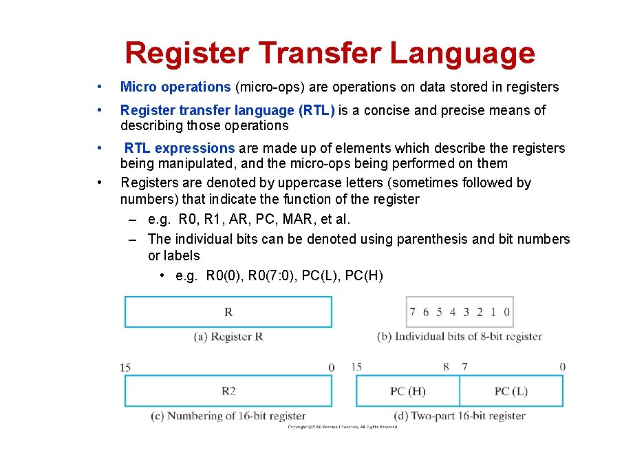
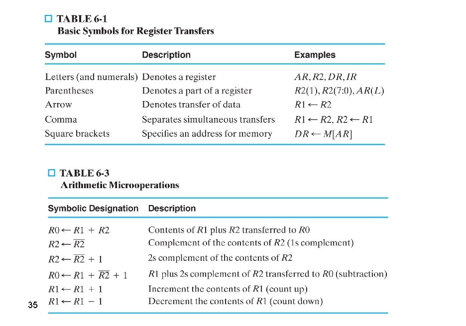
Register Transfer Language • Micro operations (micro-ops) are operations on data stored in registers • Register transfer language (RTL) is a concise and precise means of describing those operations • RTL expressions are made up of elements which describe the registers being manipulated, and the micro-ops being performed on them Registers are denoted by uppercase letters (sometimes followed by numbers) that indicate the function of the register – e. g. R 0, R 1, AR, PC, MAR, et al. – The individual bits can be denoted using parenthesis and bit numbers or labels • e. g. R 0(0), R 0(7: 0), PC(L), PC(H) •

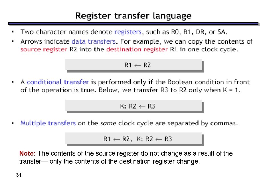
Note: The contents of the source register do not change as a result of the transfer— only the contents of the destination register change. 31

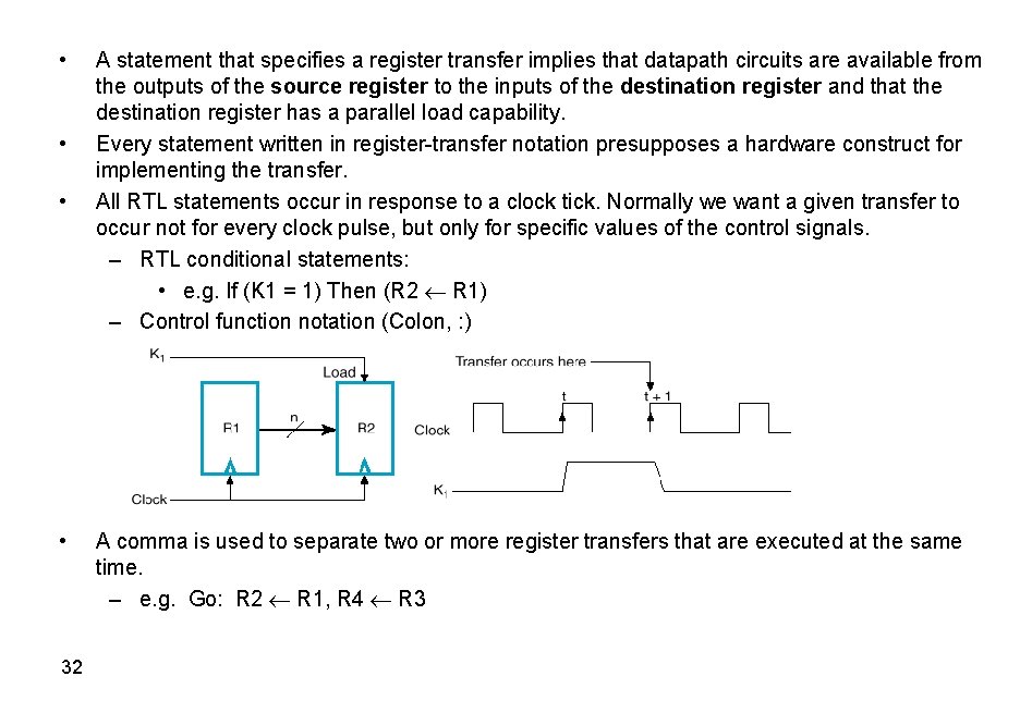
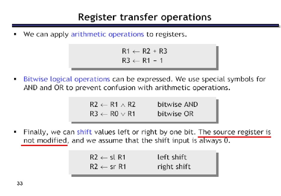
• • 32 A statement that specifies a register transfer implies that datapath circuits are available from the outputs of the source register to the inputs of the destination register and that the destination register has a parallel load capability. Every statement written in register-transfer notation presupposes a hardware construct for implementing the transfer. All RTL statements occur in response to a clock tick. Normally we want a given transfer to occur not for every clock pulse, but only for specific values of the control signals. – RTL conditional statements: • e. g. If (K 1 = 1) Then (R 2 R 1) – Control function notation (Colon, : ) • e. g. K 1: R 2 R 1 A comma is used to separate two or more register transfers that are executed at the same time. – e. g. Go: R 2 R 1, R 4 R 3

33

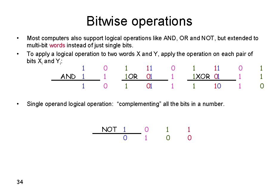
Bitwise operations • • Most computers also support logical operations like AND, OR and NOT, but extended to multi-bit words instead of just single bits. To apply a logical operation to two words X and Y, apply the operation on each pair of bits Xi and Yi: 1 AND 1 1 • 0 1 1 OR 1 0 1 11 1 XOR 01 1 10 Single operand logical operation: “complementing” all the bits in a number. NOT 1 0 34 11 01 01 0 1 0 0 1 1 0

35

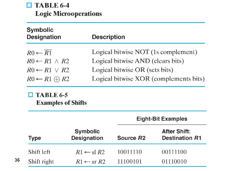
36