College of Computer and Information Sciences Department of
- Slides: 28

College of Computer and Information Sciences Department of Computer Science CSC 220: Computer Organization Unit 11 Datapath Design 1

Unit 11: Datapath Design Overview • Register file • Function Unit • ALU • Combinational Shifter • Basic Datapaths Design • General Datapath Representation • Accessing RAM • The Control Word Chapter-8 M. Morris Mano, Charles R. Kime and Tom Martin, Logic and Computer Design Fundamentals, Global (5 th) Edition, Pearson Education Limited, 2016. ISBN: 9781292096124

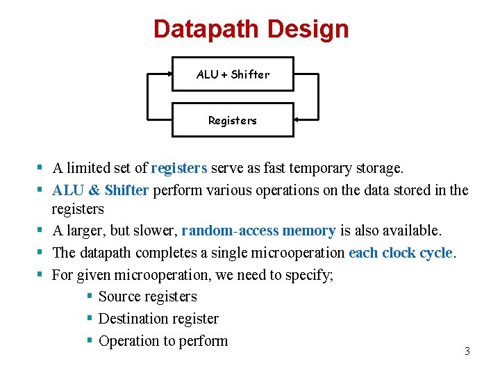
Datapath Design ALU + Shifter Registers § A limited set of registers serve as fast temporary storage. § ALU & Shifter perform various operations on the data stored in the registers § A larger, but slower, random-access memory is also available. § The datapath completes a single microoperation each clock cycle. § For given microoperation, we need to specify; § Source registers § Destination register § Operation to perform 3

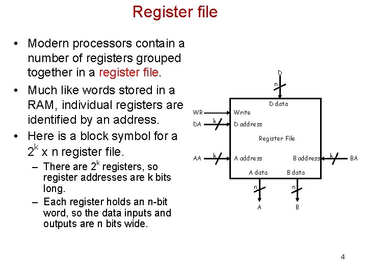
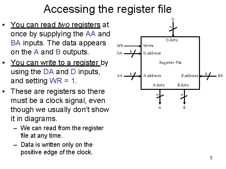
Register file • Modern processors contain a number of registers grouped together in a register file. • Much like words stored in a RAM, individual registers are identified by an address. • Here is a block symbol for a 2 k x n register file. k – There are 2 registers, so register addresses are k bits long. – Each register holds an n-bit word, so the data inputs and outputs are n bits wide. D n D data WR DA Write k D address Register File AA k A address A data n A B address k BA B data n B 4

Accessing the register file • You can read two registers at once by supplying the AA and BA inputs. The data appears on the A and B outputs. • You can write to a register by using the DA and D inputs, and setting WR = 1. • These are registers so there must be a clock signal, even though we usually don’t show it in diagrams. – We can read from the register file at any time. – Data is written only on the positive edge of the clock. D n D data WR DA Write k D address Register File AA k A address B address A data B data n n A k BA B 5

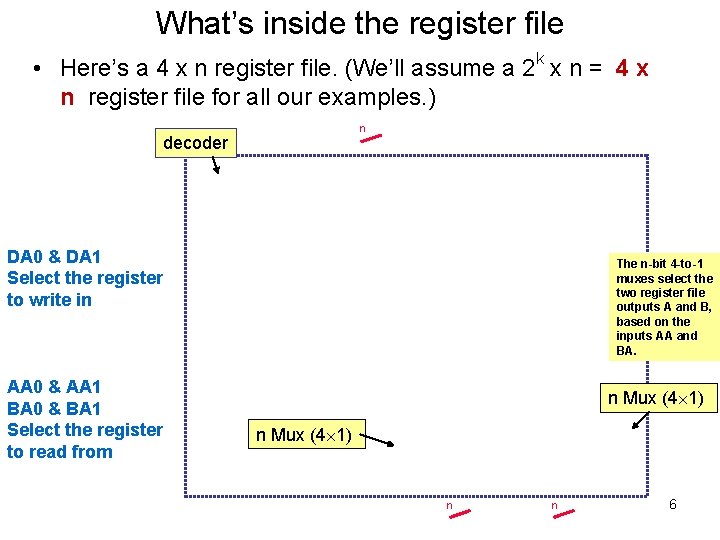
What’s inside the register file • Here’s a 4 x n register file. (We’ll assume a 2 k x n = 4 x n register file for all our examples. ) n decoder DA 0 & DA 1 Select the register to write in AA 0 & AA 1 BA 0 & BA 1 Select the register to read from The n-bit 4 -to-1 muxes select the two register file outputs A and B, based on the inputs AA and BA. BA n Mux (4 1) n n 6

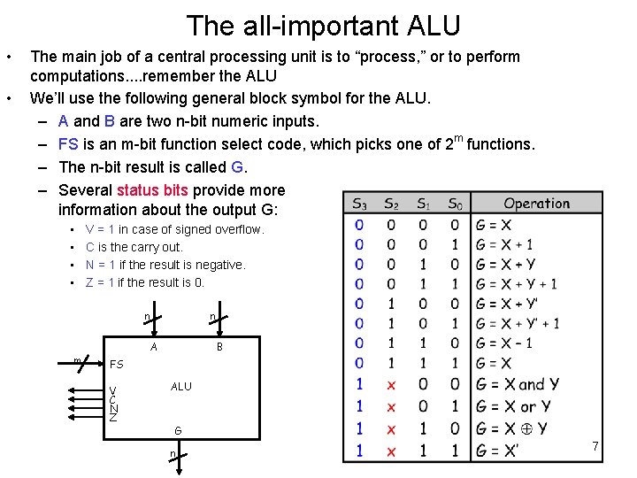
The all-important ALU • • The main job of a central processing unit is to “process, ” or to perform computations. . remember the ALU We’ll use the following general block symbol for the ALU. – A and B are two n-bit numeric inputs. – FS is an m-bit function select code, which picks one of 2 m functions. – The n-bit result is called G. – Several status bits provide more information about the output G: • • V = 1 in case of signed overflow. C is the carry out. N = 1 if the result is negative. Z = 1 if the result is 0. n m n A B FS V C N Z ALU G n 7

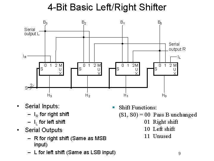
Combinational Shifter • Bidirectional shift register with parallel load – Disadvantage: 3 clock pulses required • Combinational Shifter – Transfer from a source to destination register – One clock cycle • Operations: Transfer, Shift Left, Shift Right • Filling of vacant positions – Here, will provide input lines or zero fill – Many options depending on instruction set 8

4 -Bit Basic Left/Right Shifter B 3 B 2 B 1 B 0 Serial output L Serial output R IR IL 0 1 2 M S U X S 0 1 2 M S U X 2 H 3 H 2 H 1 H 0 • Serial Inputs: § Shift Functions: – IR for right shift (S 1, S 0) = 00 Pass B unchanged 01 Right shift – IL for left shift 10 Left shift • Serial Outputs 11 Unused – R for right shift (Same as MSB input) – L for left shift (Same as LSB input) 9

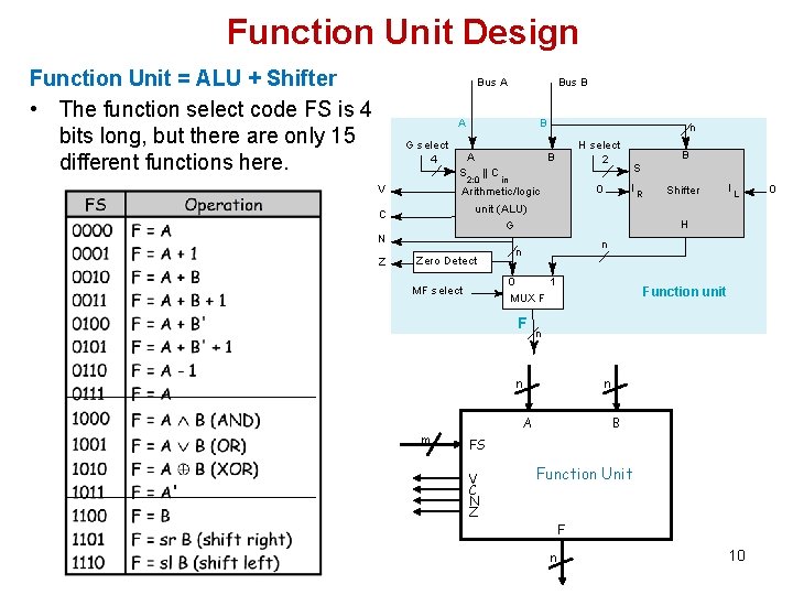
Function Unit Design Function Unit = ALU + Shifter • The function select code FS is 4 bits long, but there are only 15 different functions here. Bus A Bus B A B G select 4 A S 2: 0 V H select 2 B || C in B S IR 0 Arithmetic/logic unit (ALU) C Zero Detect F Function unit n n m IL n n 0 1 MUX F MF select Shifter H G N Z n n A B FS V C N Z Function Unit F n 10 0

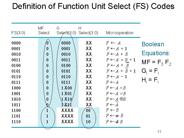
Definition of Function Unit Select (FS) Codes G Select, H Select, and MF in T of FS Codes FS(3: 0) 0000 0001 0010 0011 0100 0101 0110 0111 1000 1001 1010 1011 1100 1101 1110 MF Select 0 0 0 1 1 1 G H Select(3: 0) 0000 0001 0010 0011 0100 0101 0110 0111 1 X 00 1 X 01 1 X 10 1 X 11 XXXX XX XX XX 00 01 10 Micr ooperation F ¬ A F ¬A + 1 F ¬A + B + 1 F ¬A - 1 F ¬A F ¬ A ÙB F ¬ A ÚB F ¬ A ÅB F ¬A F ¬B F ¬ sr B F ¬ sl B Boolean Equations: MF = F 3 F 2 Gi = F i Hi = F i 11

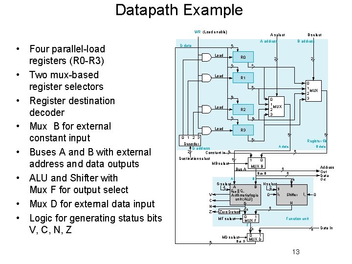
Basic Datapaths Design • Guiding principles for basic datapaths: – The set of registers • A set of registers with common access resources called a register file – Microoperation implementation • One or more shared resources for implementing microoperations • Buses - shared transfer paths • Arithmetic-Logic Unit (ALU) - shared resource for implementing arithmetic and logic microoperations • Shifter - shared resource for implementing shift microoperations 12

Datapath Example WR (Load enable) • Four parallel-load registers (R 0 -R 3) • Two mux-based register selectors • Register destination decoder • Mux B for external constant input • Buses A and B with external address and data outputs • ALU and Shifter with Mux F for output select • Mux D for external data input • Logic for generating status bits V, C, N, Z A select n D data B select A address Load R 0 B address 2 n Load R 1 0 1 MUX 2 3 n n 0 1 Load 2 3 R 2 n n Load MUX R 3 n 0 1 2 3 n n Decoder D address 2 Constant in n Destination select n MB select Register file A data 1 Bus A 0 MUX B A n C N Z B G select A B 4 S 2: 0 || Cin Arithmetic/logic unit (ALU) G n Zero Detect 0 1 MUX F F n MF select MD select n Bus D Address Out Data n Bus B V B data n H select 2 S 0 IR Out n B Shifter IL 0 H n Function unit n 0 1 MUX D 13 Data In

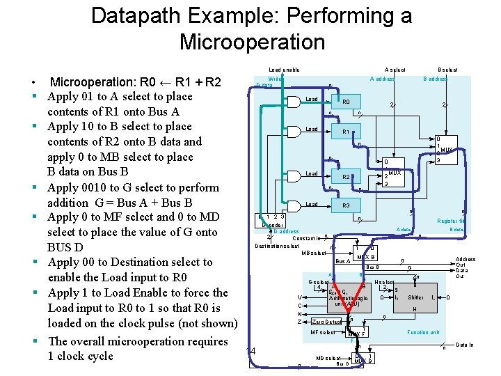
Datapath Example: Performing a Microoperation Load enable • Microoperation: R 0 ← R 1 + R 2 § Apply 01 to A select to place contents of R 1 onto Bus A § Apply 10 to B select to place contents of R 2 onto B data and apply 0 to MB select to place B data on Bus B § Apply 0010 to G select to perform addition G = Bus A + Bus B § Apply 0 to MF select and 0 to MD select to place the value of G onto BUS D § Apply 00 to Destination select to enable the Load input to R 0 § Apply 1 to Load Enable to force the Load input to R 0 to 1 so that R 0 is loaded on the clock pulse (not shown) § The overall microoperation requires 1 clock cycle A select Write D data B select A address n Load R 0 B address 2 n Load R 1 0 1 MUX 2 3 n n 0 1 Load 2 3 R 2 n n Load MUX R 3 n 0 1 2 3 n n Decoder D address 2 Constant in n Destination select n MB select Register file A data 1 Bus A 0 MUX B A n C N Z B G select A B 4 S 2: 0 || Cin Arithmetic/logic unit (ALU) G 0 1 MUX F F n MF select 14 n Zero Detect MD select n Bus D 0 1 MUX D Address Out Data n Bus B V B data n H select 2 S 0 IR Out n B Shifter IL 0 H n Function unit n Data In

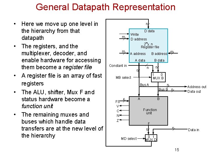
General Datapath Representation • Here we move up one level in the hierarchy from that datapath • The registers, and the multiplexer, decoder, and enable hardware for accessing them become a register file • A register file is an array of fast registers • The ALU, shifter, Mux F and status hardware become a function unit • The remaining muxes and buses which handle data transfers are at the new level of the hierarchy n m m D data Write D address 2 mx n Register file A address B address A data Constant in B data n n n 1 0 MUX B MB select Bus A FS V C N Z 4 m A n Bus B n Address out Data out B Function unit F n MD select n Data in 0 1 MUX D 15

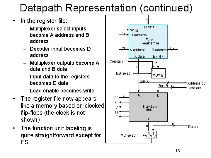
Datapath Representation (continued) • In the register file: – Multiplexer select inputs become A address and B address – Decoder input becomes D address – Multiplexer outputs become A data and B data – Input data to the registers becomes D data – Load enable becomes write • The register file now appears like a memory based on clocked flip-flops (the clock is not shown) • The function unit labeling is quite straightforward except for FS n m m D data Write D address 2 mx n Register file A address B address A data Constant in B data n n n 1 0 MUX B MB select Bus A FS V C N Z 4 m A n Bus B n Address out Data out B Function unit F n MD select n Data in 0 1 MUX D 16

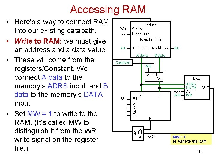
Accessing RAM • Here’s a way to connect RAM into our existing datapath. • Write to RAM: we must give an address and a data value. • These will come from the registers/Constant. We connect A data to the memory’s ADRS input, and B data to the memory’s DATA input. • Set MW = 1 to write to the RAM. (It’s called MW to distinguish it from the WR write signal on the register file. ) WR DA D data Write D address Register File AA A address B address A data Constant BA B data MB S D 1 D 0 Q FS FS V C N Z A D 0 Q D 1 S B +5 V MW RAM ADRS DATA OUT CS WR F MD MW = 1 to write to the RAM 17

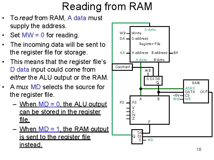
Reading from RAM • To read from RAM, A data must supply the address. • Set MW = 0 for reading. • The incoming data will be sent to the register file for storage. • This means that the register file’s D data input could come from either the ALU output or the RAM. • A mux MD selects the source for the register file. – When MD = 0, the ALU output can be stored in the register file. – When MD = 1, the RAM output is sent to the register file instead. WR DA D data Write D address Register File AA A address B address A data Constant BA B data MB S D 1 D 0 Q FS FS A V C N Z D 0 Q D 1 S B +5 V MW RAM ADRS DATA OUT CS WR F MD 18

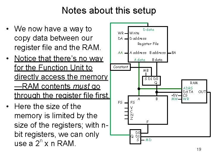
Notes about this setup • We now have a way to copy data between our register file and the RAM. • Notice that there’s no way for the Function Unit to directly access the memory —RAM contents must go through the register file first. • Here the size of the memory is limited by the size of the registers; with nbit registers, we can only use a 2 n x n RAM. WR DA D data Write D address Register File AA A address B address A data Constant BA B data MB S D 1 D 0 Q FS FS A V C N Z D 0 Q D 1 S B +5 V MW RAM ADRS DATA OUT CS WR F MD 19

Datapath (Summary) § The datapath completes a single microoperation each clock cycle. § For given microoperation, we need to specify; § Source registers § Destination register § Operation to perform § For the datapath, we also need to specify; § External or function data § Data B from register or constant § Whether the destination is updated 20

The Control Word • The datapath has many control inputs • The signals driving these inputs can be defined and organized into a control word • To execute a microinstruction, we apply control word values for a clock cycle. For most microoperations, the positive edge of the clock cycle is needed to perform the register load • The datapath control word format and the field definitions are shown on the next slide 21

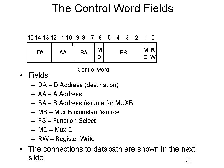
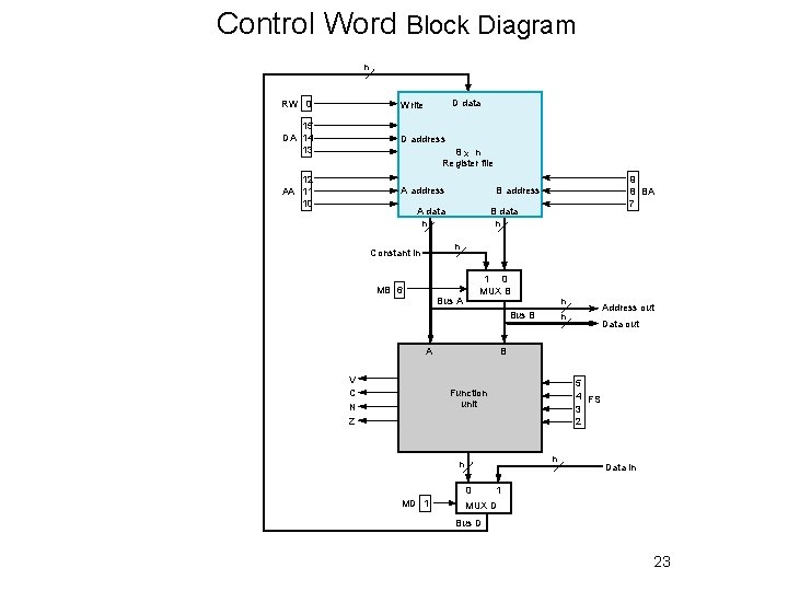
The Control Word Fields 15 14 13 12 11 10 9 8 7 6 DA • Fields – – – – AA BA 5 M B 4 3 FS 2 1 0 M R D W Control word DA – D Address (destination) AA – A Address BA – B Address (source for MUXB MB – Mux B (constant/source FS – Function Select MD – Mux D RW – Register Write • The connections to datapath are shown in the next slide 22

Control Word Block Diagram n D data RW 0 Write 15 DA 14 13 D address 12 AA 11 10 A address 8 x n Register file 9 8 BA 7 B address A data n B data n n Constant in MB 6 1 0 MUX B Bus A n n Bus B A V C N Z Data out B 5 4 FS 3 2 Function unit n n 0 MD 1 Address out Data in 1 MUX D Bus D 23

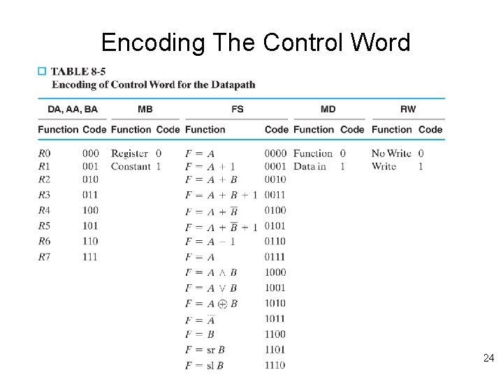
Encoding The Control Word 24

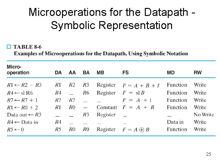
Microoperations for the Datapath Symbolic Representation 25

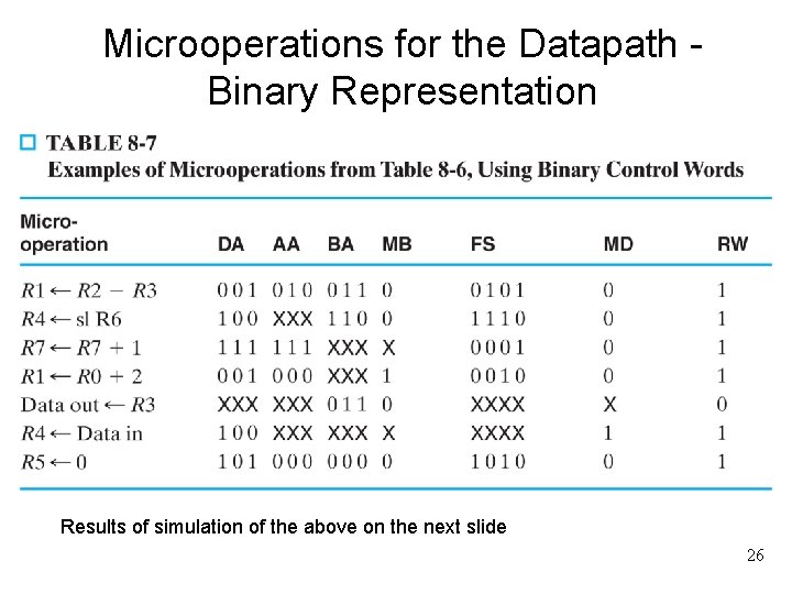
Microoperations for the Datapath Binary Representation Results of simulation of the above on the next slide 26

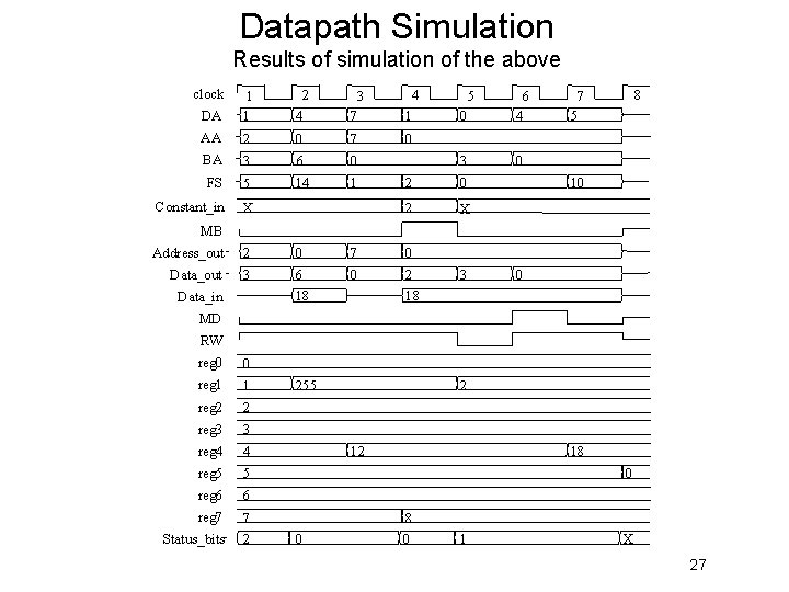
Datapath Simulation Results of simulation of the above clock 2 4 3 7 4 1 2 0 7 0 BA 3 6 0 FS 5 14 1 Constant_in X DA 1 1 AA 5 0 6 4 3 0 2 X 8 7 5 10 MB Address_out 2 0 7 0 Data_out 3 6 0 2 18 Data_in 3 0 18 MD RW reg 0 reg 1 0 1 reg 2 2 reg 3 3 reg 4 4 reg 5 5 reg 6 6 reg 7 7 Status_bits 2 255 2 12 18 0 0 1 X 27

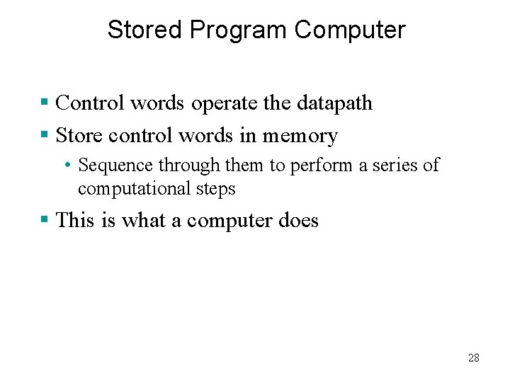
Stored Program Computer § Control words operate the datapath § Store control words in memory • Sequence through them to perform a series of computational steps § This is what a computer does 28