College of Computer and Information Sciences Department of
- Slides: 21

College of Computer and Information Sciences Department of Computer Science CSC 220: Computer Organization Unit 7 Sequential Circuits (Flip Flop)

Unit 7: Sequential Circuits Overview • SR Latch • SR Latch with Control Input • D Latch • Clock and Synchronization • Flip-flops • Positive edge-triggered D Flip- flop • JK &T Flip-flop • Direct Inputs Chapter-4 M. Morris Mano, Charles R. Kime and Tom Martin, Logic and Computer Design Fundamentals, Global (5 th) Edition, Pearson Education Limited, 2016. ISBN: 9781292096124

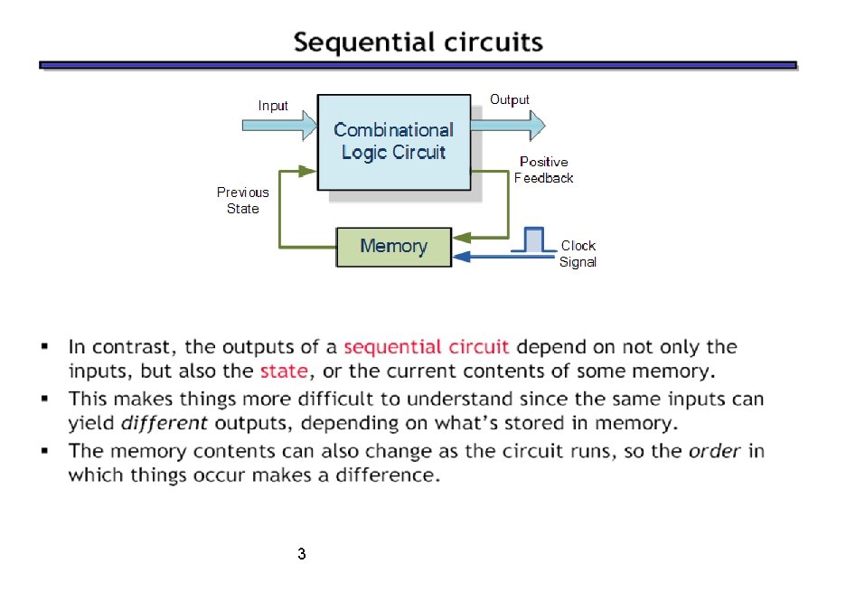
3

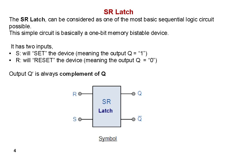
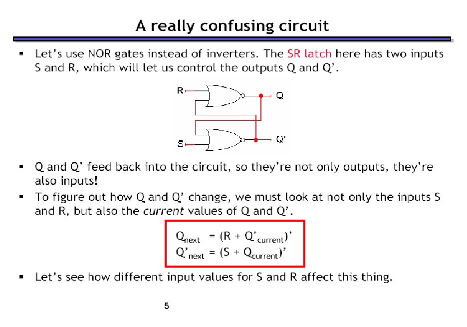
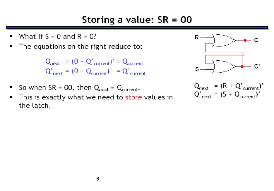
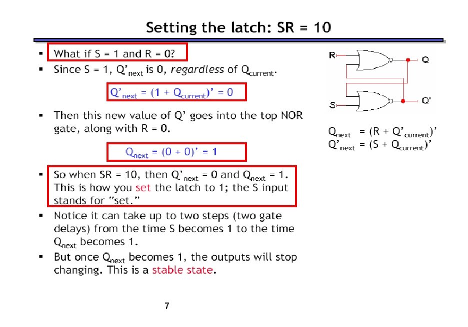
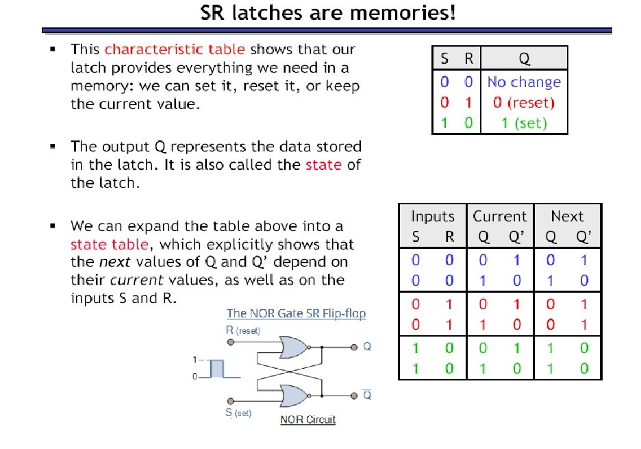
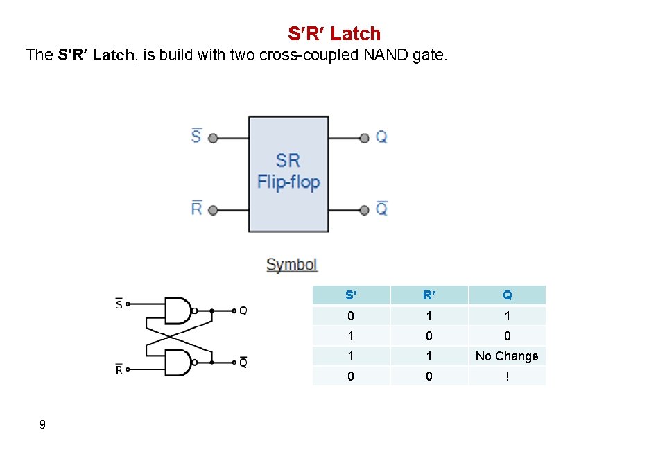
SR Latch The SR Latch, can be considered as one of the most basic sequential logic circuit possible. This simple circuit is basically a one-bit memory bistable device. It has two inputs, • S: will “SET” the device (meaning the output Q = “ 1”) • R: will “RESET” the device (meaning the output Q = “ 0”) Output Q is always complement of Q 4

5

6

7

8

S R Latch The S R Latch, is build with two cross-coupled NAND gate. 9 S R Q 0 1 1 1 0 0 1 1 No Change 0 0 !

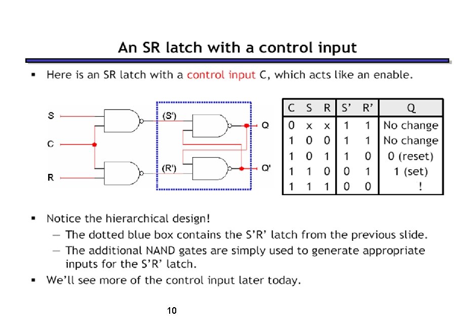
10

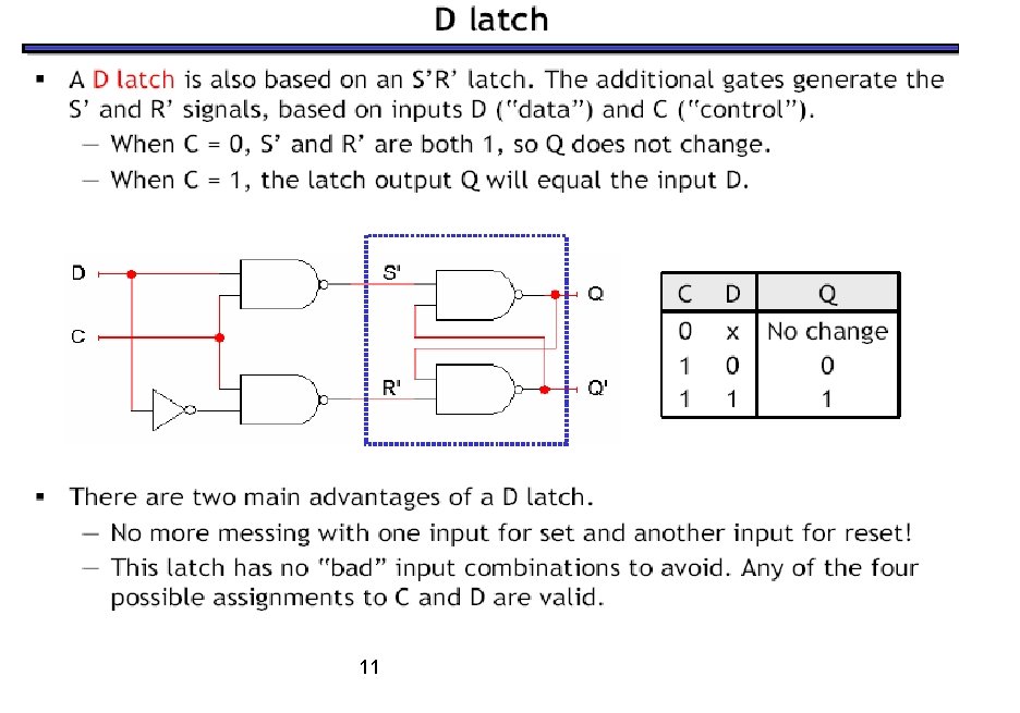
11

Give Examples 12

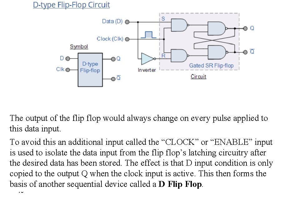
The output of the flip flop would always change on every pulse applied to this data input. To avoid this an additional input called the “CLOCK” or “ENABLE” input is used to isolate the data input from the flip flop’s latching circuitry after the desired data has been stored. The effect is that D input condition is only copied to the output Q when the clock input is active. This then forms the basis of another sequential device called a D Flip Flop. 13

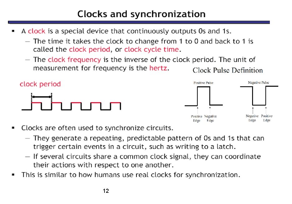
14

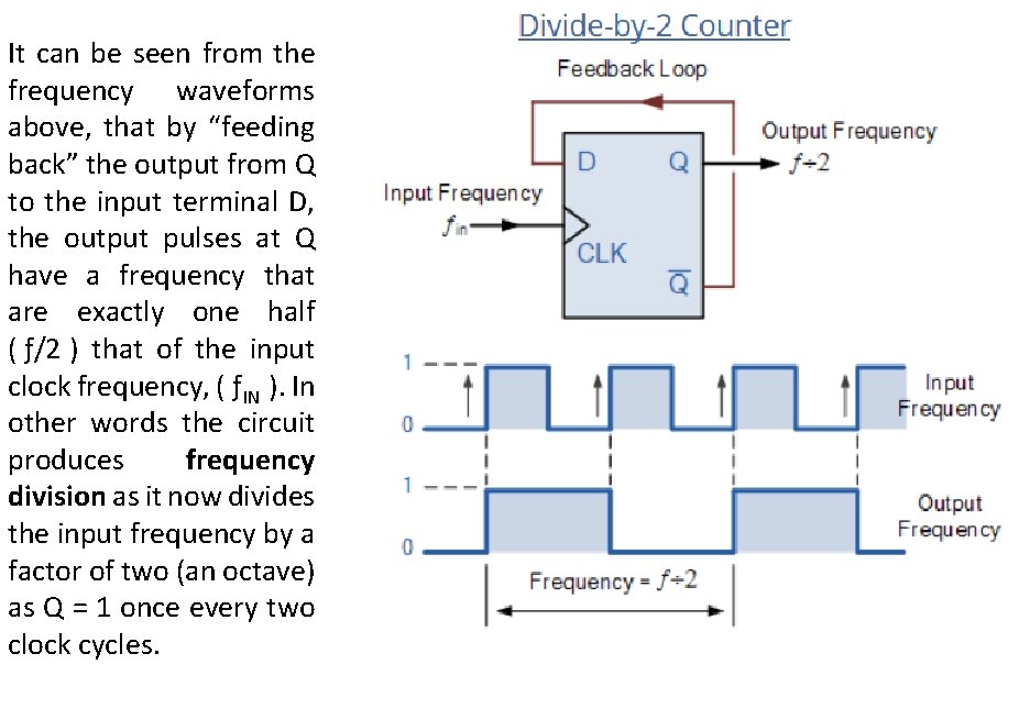
It can be seen from the frequency waveforms above, that by “feeding back” the output from Q to the input terminal D, the output pulses at Q have a frequency that are exactly one half ( ƒ/2 ) that of the input clock frequency, ( ƒIN ). In other words the circuit produces frequency division as it now divides the input frequency by a factor of two (an octave) as Q = 1 once every two clock cycles. 15

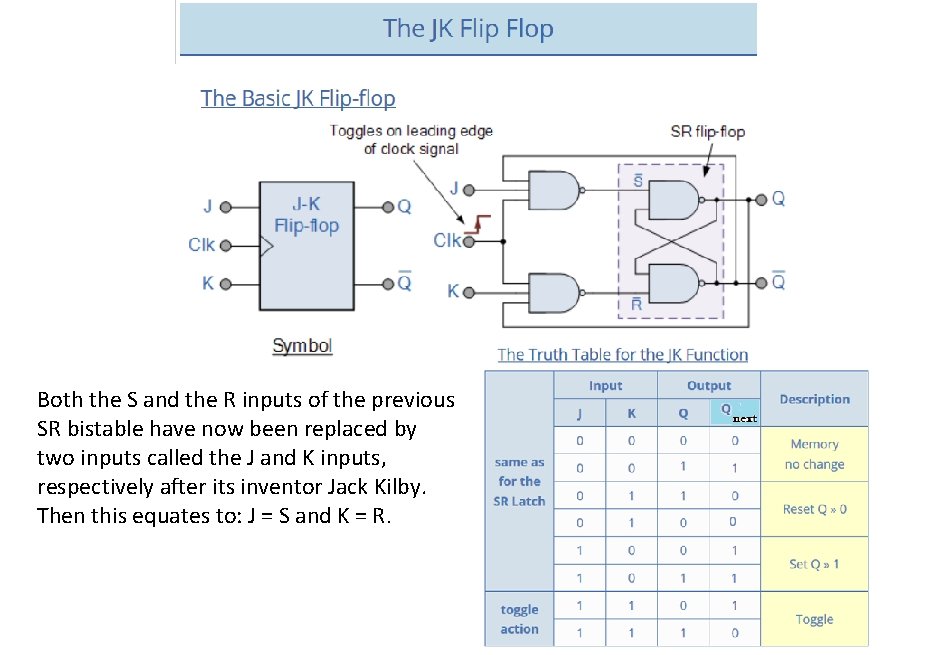
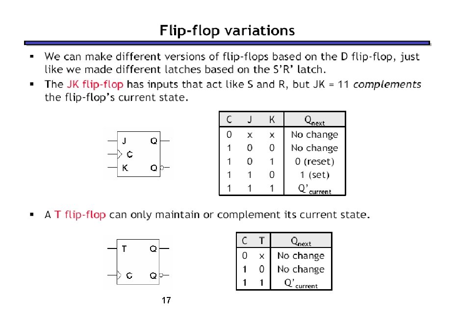
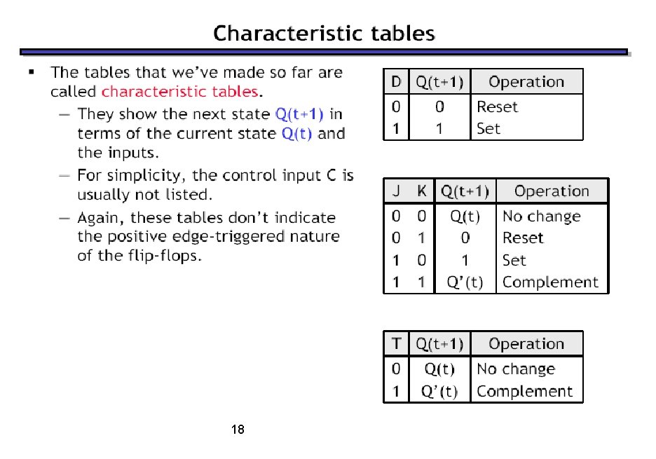
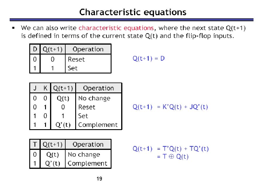
Both the S and the R inputs of the previous SR bistable have now been replaced by two inputs called the J and K inputs, respectively after its inventor Jack Kilby. Then this equates to: J = S and K = R.

17

18

19

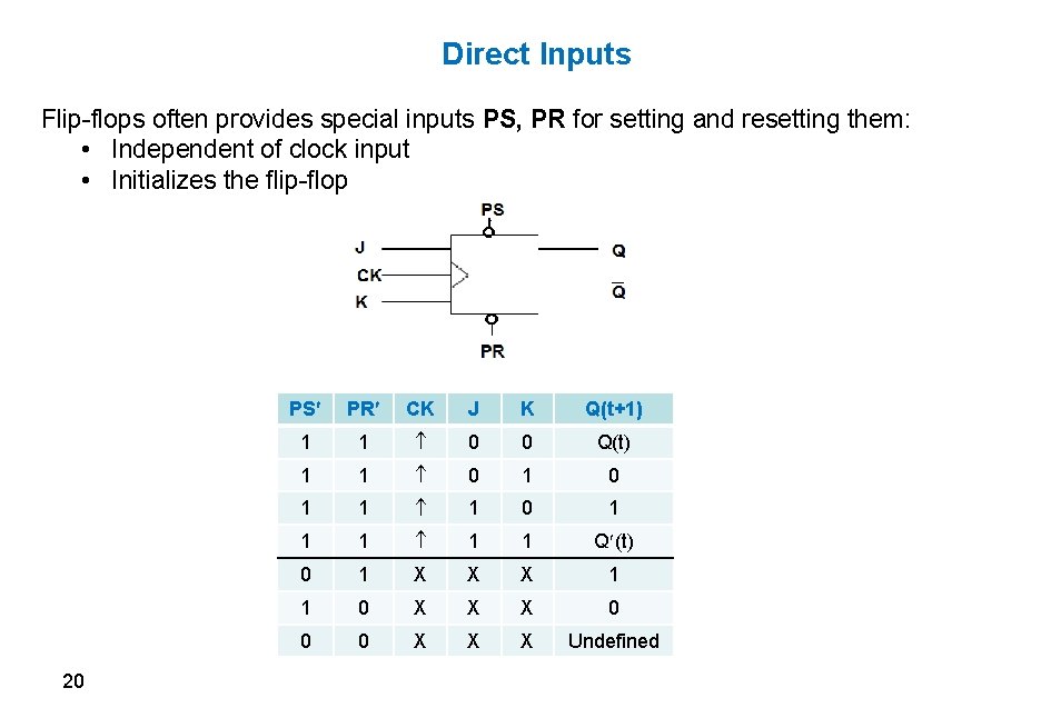
Direct Inputs Flip-flops often provides special inputs PS, PR for setting and resetting them: • Independent of clock input • Initializes the flip-flop 20 PS PR CK J K Q(t+1) 1 1 0 0 Q(t) 1 1 0 1 1 1 Q (t) 0 1 X X X 1 1 0 X X X 0 0 0 X X X Undefined

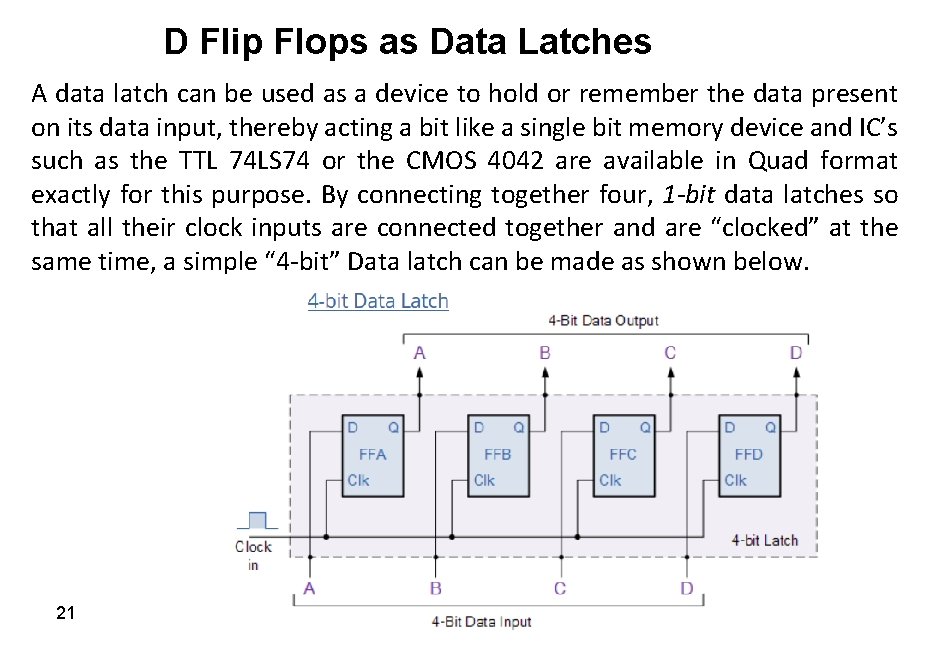
D Flip Flops as Data Latches A data latch can be used as a device to hold or remember the data present on its data input, thereby acting a bit like a single bit memory device and IC’s such as the TTL 74 LS 74 or the CMOS 4042 are available in Quad format exactly for this purpose. By connecting together four, 1 -bit data latches so that all their clock inputs are connected together and are “clocked” at the same time, a simple “ 4 -bit” Data latch can be made as shown below. 21