Chapter 4 Interconnect Polysilicon for Local Connections WL0
![Polysilicon for Local Connections WL[0] Transistor (2 l x 4 l) GND WL[1] ROM Polysilicon for Local Connections WL[0] Transistor (2 l x 4 l) GND WL[1] ROM](https://slidetodoc.com/presentation_image_h/1edfd3243ee66177404b68d45eb5a9ad/image-2.jpg)
- Slides: 23

Chapter 4 Interconnect
![Polysilicon for Local Connections WL0 Transistor 2 l x 4 l GND WL1 ROM Polysilicon for Local Connections WL[0] Transistor (2 l x 4 l) GND WL[1] ROM](https://slidetodoc.com/presentation_image_h/1edfd3243ee66177404b68d45eb5a9ad/image-2.jpg)
Polysilicon for Local Connections WL[0] Transistor (2 l x 4 l) GND WL[1] ROM Layout Polysilicon WL[2] GND WL[3] Metal 1 Diffusion Metal 1 on Diffusion Copyright © 2005 Pearson Addison-Wesley. All rights reserved. 4 -2

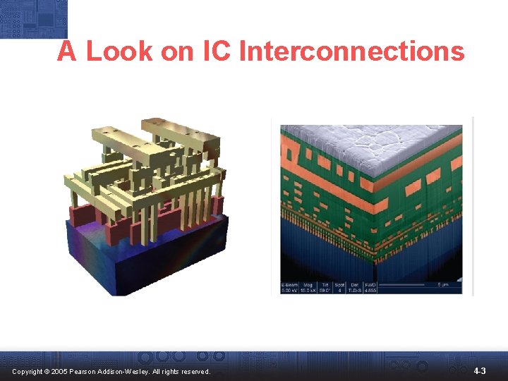
A Look on IC Interconnections Copyright © 2005 Pearson Addison-Wesley. All rights reserved. 4 -3

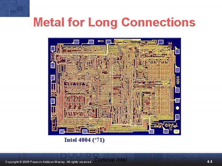
Metal for Long Connections Intel 4004 (‘ 71) Copyright © 2005 Pearson Addison-Wesley. All rights reserved. Cortesia Intel 4 -4

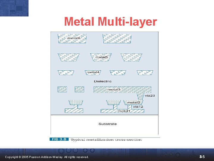
Metal Multi-layer Copyright © 2005 Pearson Addison-Wesley. All rights reserved. 4 -5 3 -5

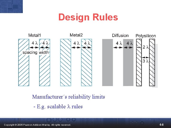
Design Rules Manufacturer´s reliability limits - E. g. scalable l rules Copyright © 2005 Pearson Addison-Wesley. All rights reserved. 4 -6

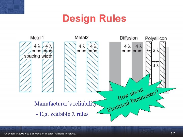
Design Rules ut rs? o b a te e w o m H Para Manufacturer´s reliability limits rical t Elec - E. g. scalable l rules Copyright © 2005 Pearson Addison-Wesley. All rights reserved. 4 -7

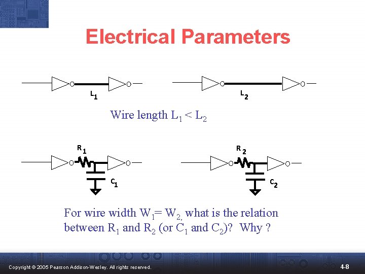
Electrical Parameters L 2 L 1 Wire length L 1 < L 2 R 1 R 2 C 1 C 2 For wire width W 1= W 2, what is the relation between R 1 and R 2 (or C 1 and C 2)? Why ? Copyright © 2005 Pearson Addison-Wesley. All rights reserved. 4 -8

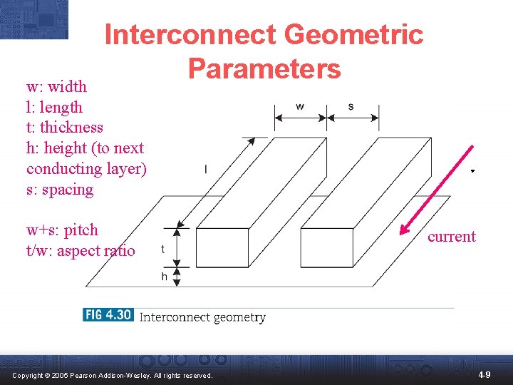
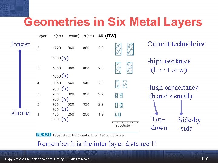
Interconnect Geometric Parameters w: width l: length t: thickness h: height (to next conducting layer) s: spacing w+s: pitch t/w: aspect ratio Copyright © 2005 Pearson Addison-Wesley. All rights reserved. current 4 -9

Geometries in Six Metal Layers (t/w) Current technoloies: longer (h) (h) shorter -high resitance (l >> t or w) -high capacitance (h and s small) (h) Topdown Side-by -side Remember h is the inter layer distance!!! Copyright © 2005 Pearson Addison-Wesley. All rights reserved. 4 -10

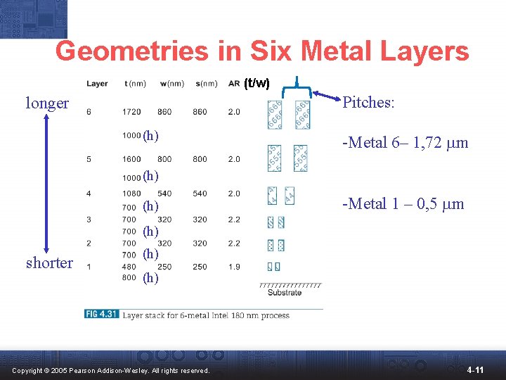
Geometries in Six Metal Layers (t/w) Pitches: longer (h) -Metal 6– 1, 72 mm (h) -Metal 1 – 0, 5 mm (h) shorter (h) Copyright © 2005 Pearson Addison-Wesley. All rights reserved. 4 -11

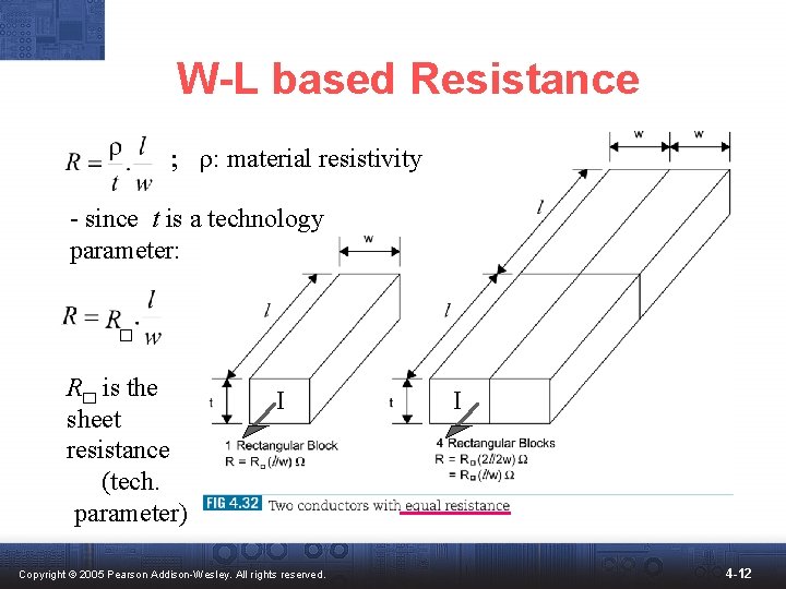
W-L based Resistance ; r: material resistivity - since t is a technology parameter: R is the sheet resistance (tech. parameter) I Copyright © 2005 Pearson Addison-Wesley. All rights reserved. I 4 -12

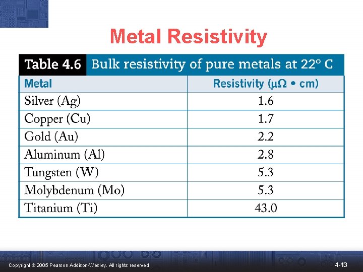
Metal Resistivity Copyright © 2005 Pearson Addison-Wesley. All rights reserved. 4 -13

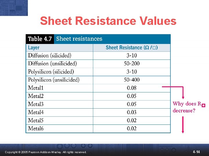
Sheet Resistance Values Why does R decrease? Copyright © 2005 Pearson Addison-Wesley. All rights reserved. 4 -14

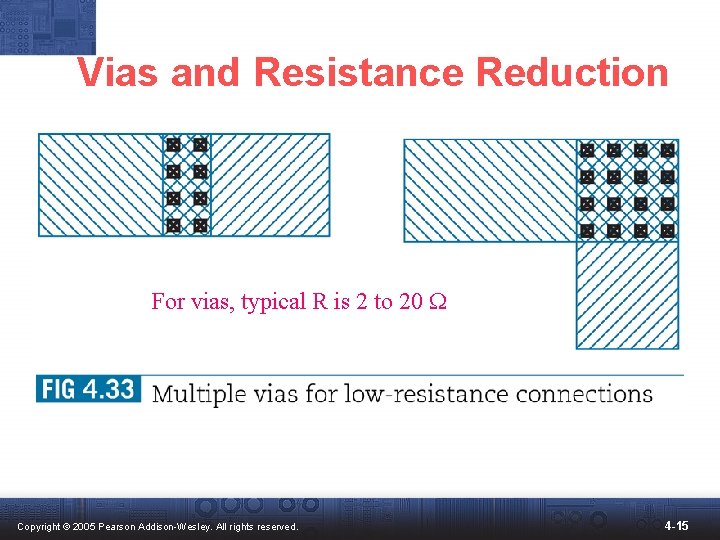
Vias and Resistance Reduction For vias, typical R is 2 to 20 W Copyright © 2005 Pearson Addison-Wesley. All rights reserved. 4 -15

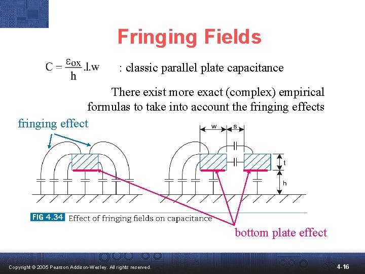
Fringing Fields : classic parallel plate capacitance There exist more exact (complex) empirical formulas to take into account the fringing effects fringing effect bottom plate effect Copyright © 2005 Pearson Addison-Wesley. All rights reserved. 4 -16

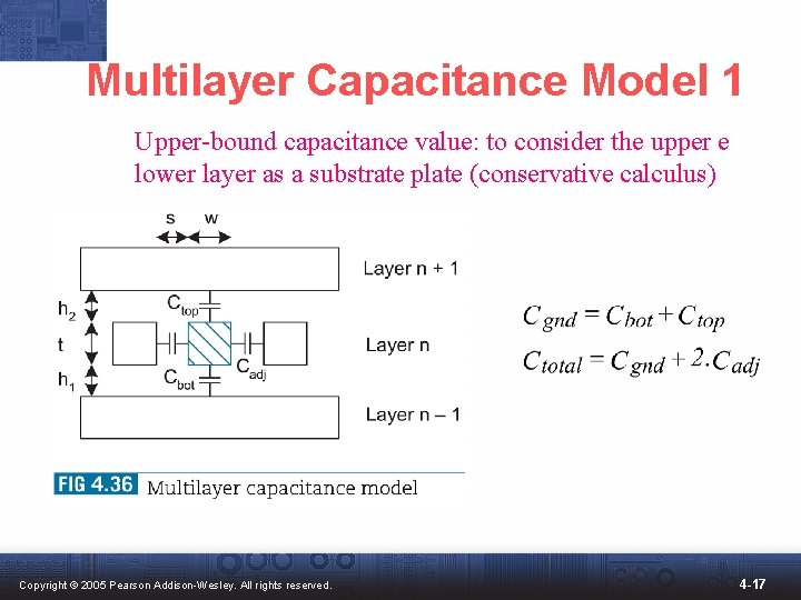
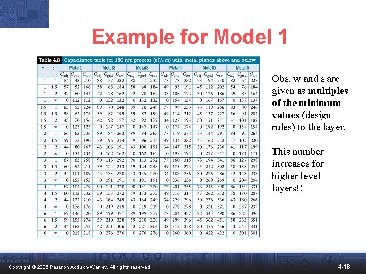
Multilayer Capacitance Model 1 Upper-bound capacitance value: to consider the upper e lower layer as a substrate plate (conservative calculus) Copyright © 2005 Pearson Addison-Wesley. All rights reserved. 4 -17

Example for Model 1 Obs. w and s are given as multiples of the minimum values (design rules) to the layer. This number increases for higher level layers!! Copyright © 2005 Pearson Addison-Wesley. All rights reserved. 4 -18

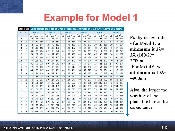
Example for Model 1 Ex. by design rules - for Metal 1, w minimum is 3 l= 3 X (180/2)= 270 nm -For Metal 6, w minimum is 10 l= =900 nm Also, the larger the width w of the plate, the larger the capacitance. Copyright © 2005 Pearson Addison-Wesley. All rights reserved. 4 -19

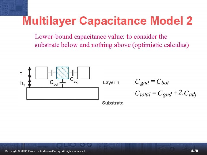
Multilayer Capacitance Model 2 Lower-bound capacitance value: to consider the substrate below and nothing above (optimistic calculus) Layer n Substrate Copyright © 2005 Pearson Addison-Wesley. All rights reserved. 4 -20

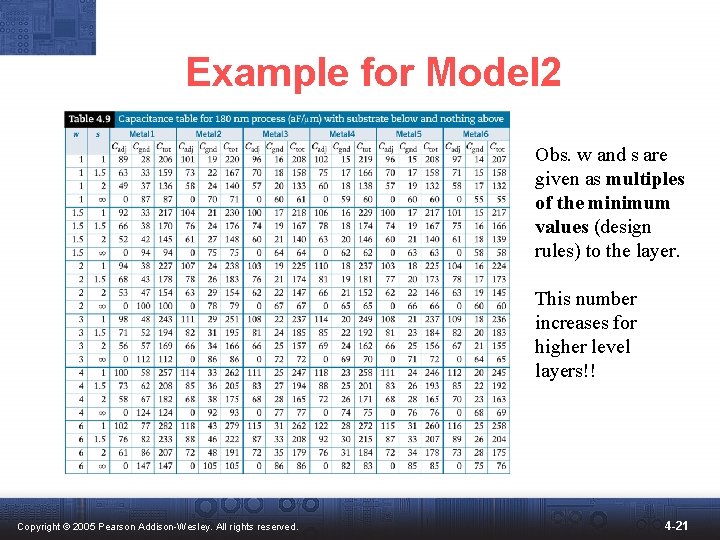
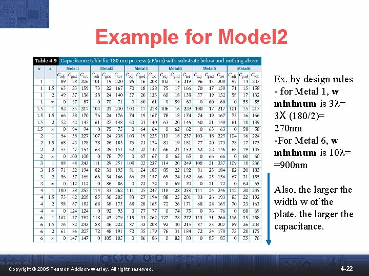
Example for Model 2 Obs. w and s are given as multiples of the minimum values (design rules) to the layer. This number increases for higher level layers!! Copyright © 2005 Pearson Addison-Wesley. All rights reserved. 4 -21

Example for Model 2 Ex. by design rules - for Metal 1, w minimum is 3 l= 3 X (180/2)= 270 nm -For Metal 6, w minimum is 10 l= =900 nm Also, the larger the width w of the plate, the larger the capacitance. Copyright © 2005 Pearson Addison-Wesley. All rights reserved. 4 -22

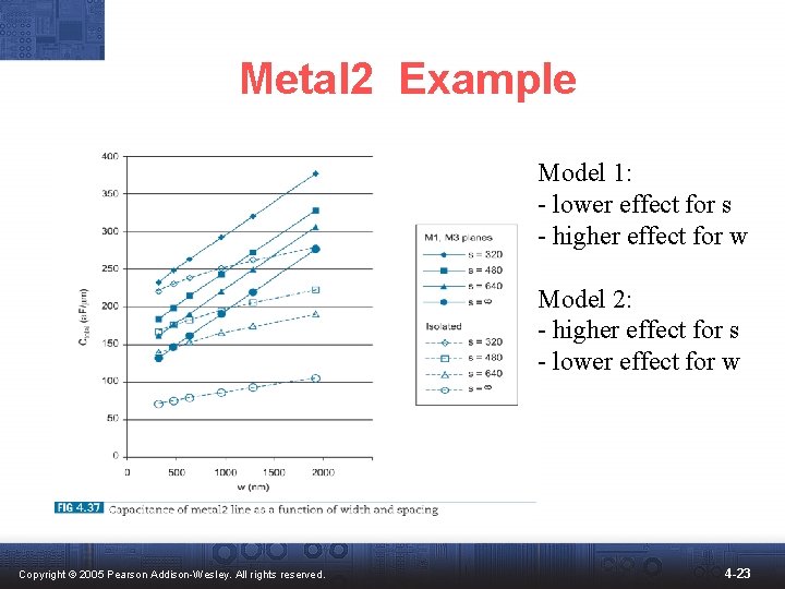
Metal 2 Example Model 1: - lower effect for s - higher effect for w Model 2: - higher effect for s - lower effect for w Copyright © 2005 Pearson Addison-Wesley. All rights reserved. 4 -23