Anisotropic magnetoresistance and spininjection Hall effect in 2

- Slides: 49

Anisotropic magnetoresistance and spin-injection Hall effect in 2 D spin-orbit coupled systems Tomas Jungwirth Institute of Physics ASCR Karel Výborný, Jan Zemen, Jan Mašek, Vít Novák, Kamil Olejník, et al. Hitachi Cambridge, Univ. Cambridge Jorg Wunderlich, Andrew Irvine, Elisa de Ranieri, Byonguk Park, et al. University of Nottingham Bryan Gallagher, Richard Campion, Kevin Edmonds, Andrew Rushforth, et al. Texas A&M Jairo Sinova, et al. University of Texas Allan Ma. Donald, et al.

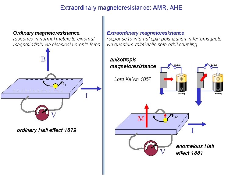
Extraordinary magnetoresistance: AMR, AHE Ordinary magnetoresistance: response in normal metals to external magnetic field via classical Lorentz force B Extraordinary magnetoresistance: response to internal spin polarization in ferromagnets via quantum-relativistic spin-orbit coupling anisotropic magnetoresistance _ _ _ Lord Kelvin 1857 FL +++++++ V I M __ FSO I ordinary Hall effect 1879 V anomalous Hall effect 1881

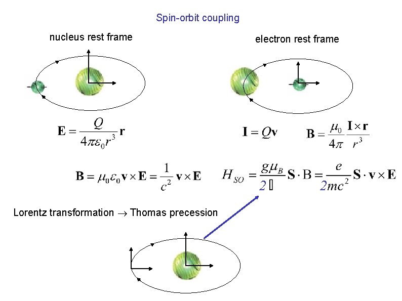
Spin-orbit coupling nucleus rest frame electron rest frame 2 Lorentz transformation Thomas precession 2

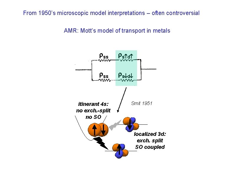
From 1950’s microscopic model interpretations – often controversial AMR: Mott’s model of transport in metals s d ss s d itinerant 4 s: no exch. -split no SO Smit 1951 localized 3 d: exch. split SO coupled

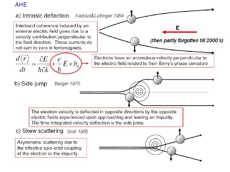
AHE Karplus&Luttinger 1954 (then partly forgotten till 2000’s) Berger 1970 Smit 1955

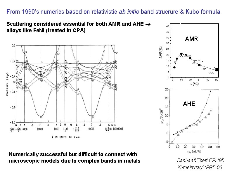
From 1990’s numerics based on relativistic ab initio band strucrure & Kubo formula Scattering considered essential for both AMR and AHE alloys like Fe. Ni (treated in CPA) AMR AHE Numerically successful but difficult to connect with microscopic models due to complex bands in metals Banhart&Ebert EPL‘ 95 Khmelevskyi ‘PRB 03

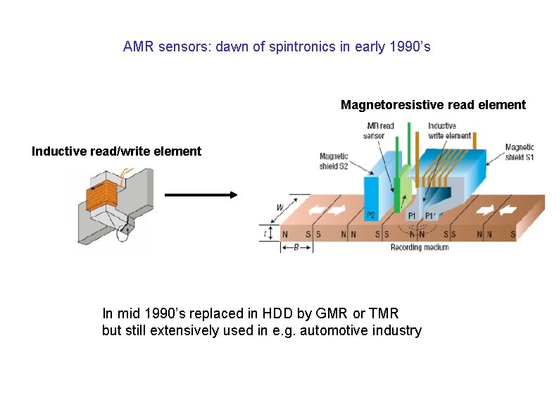
AMR sensors: dawn of spintronics in early 1990’s Magnetoresistive read element Inductive read/write element In mid 1990’s replaced in HDD by GMR or TMR but still extensively used in e. g. automotive industry

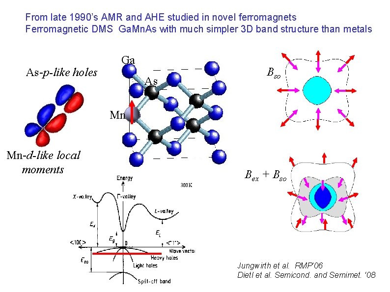
From late 1990’s AMR and AHE studied in novel ferromagnets Ferromagnetic DMS Ga. Mn. As with much simpler 3 D band structure than metals As-p-like holes Ga As Bso Mn Mn-d-like local moments Bex + Bso Jungwirth et al. RMP’ 06 Dietl et al. Semicond. and Semimet. ‘ 08

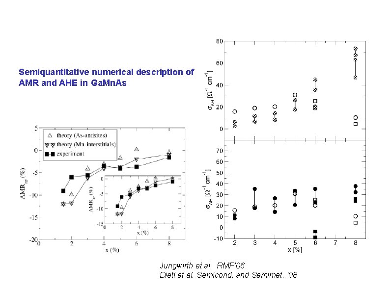
Semiquantitative numerical description of AMR and AHE in Ga. Mn. As Jungwirth et al. RMP’ 06 Dietl et al. Semicond. and Semimet. ‘ 08

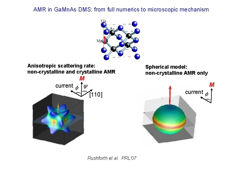
AMR in Ga. Mn. As DMS: from full numerics to microscopic mechanism Anisotropic scattering rate: non-crystalline and crystalline AMR M M [110] current ) ) ) current Spherical model: non-crystalline AMR only Rushforth et al. PRL‘ 07

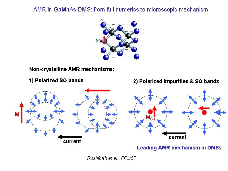
AMR in Ga. Mn. As DMS: from full numerics to microscopic mechanism Non-crystalline AMR mechanisms: 1) Polarized SO bands 2) Polarized impurities & SO bands M MGa current Leading AMR mechanism in DMSs Rushforth et al. PRL‘ 07

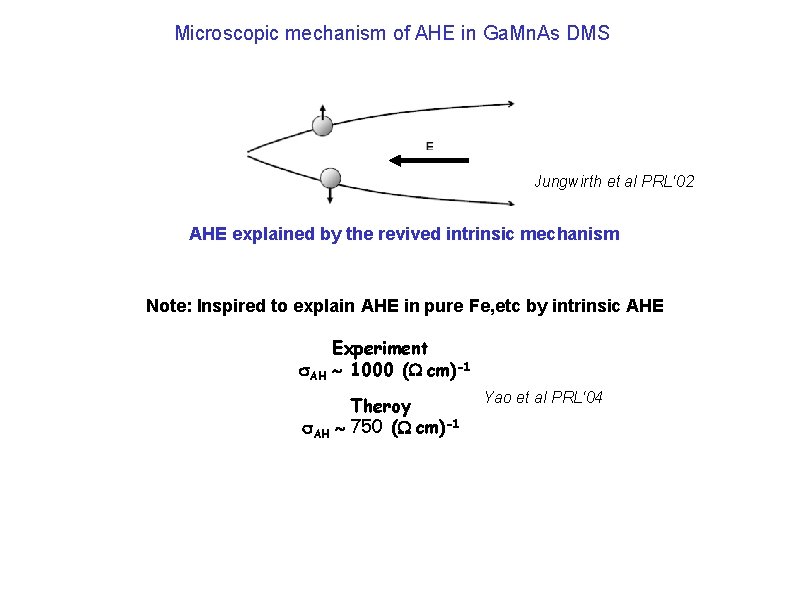
Microscopic mechanism of AHE in Ga. Mn. As DMS Jungwirth et al PRL‘ 02 AHE explained by the revived intrinsic mechanism Note: Inspired to explain AHE in pure Fe, etc by intrinsic AHE Experiment AH 1000 (W cm)-1 Theroy AH 750 (W cm)-1 Yao et al PRL‘ 04

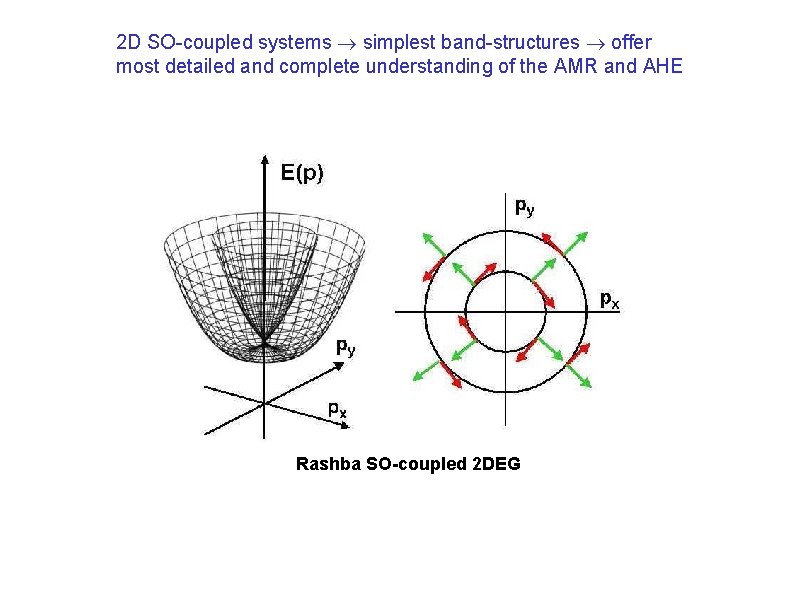
2 D SO-coupled systems simplest band-structures offer most detailed and complete understanding of the AMR and AHE Rashba SO-coupled 2 DEG

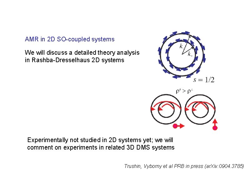
AMR in 2 D SO-coupled systems We will discuss a detailed theory analysis in Rashba-Dresselhaus 2 D systems Experimentally not studied in 2 D systems yet; we will comment on experiments in related 3 D DMS systems Trushin, Vyborny et al PRB in press (ar. Xiv: 0904. 3785)

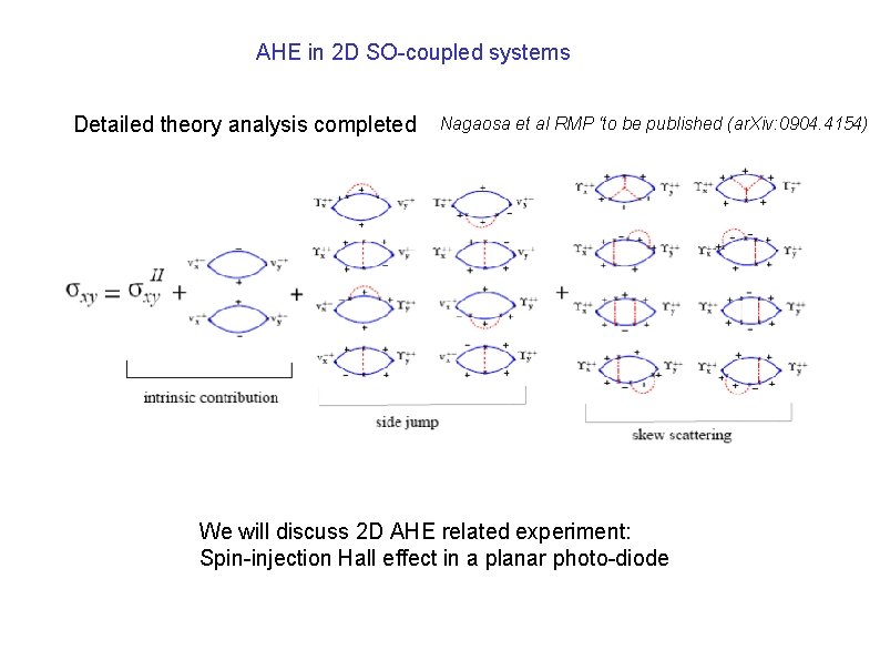
AHE in 2 D SO-coupled systems Detailed theory analysis completed Nagaosa et al RMP ‘to be published (ar. Xiv: 0904. 4154) We will discuss 2 D AHE related experiment: Spin-injection Hall effect in a planar photo-diode

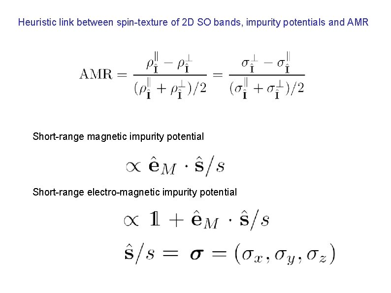
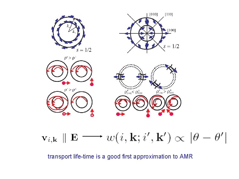
Heuristic link between spin-texture of 2 D SO bands, impurity potentials and AMR Short-range magnetic impurity potential Short-range electro-magnetic impurity potential

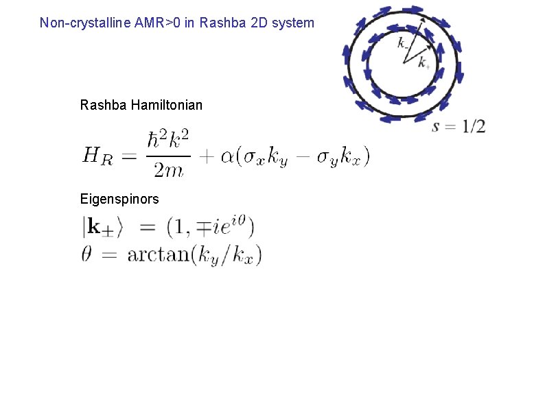
Non-crystalline AMR>0 in Rashba 2 D system Rashba Hamiltonian Eigenspinors

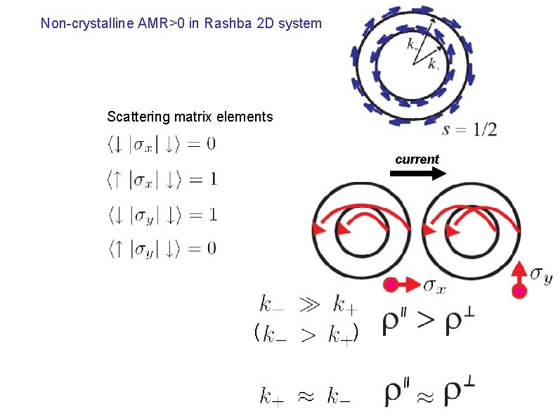
Non-crystalline AMR>0 in Rashba 2 D system Scattering matrix elements current ( )

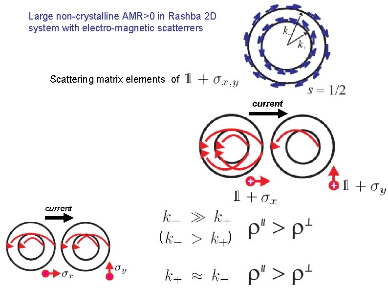
Large non-crystalline AMR>0 in Rashba 2 D system with electro-magnetic scatterrers Scattering matrix elements of current ( )

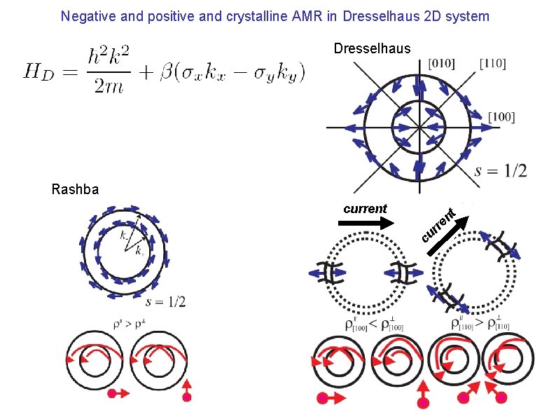
Negative and positive and crystalline AMR in Dresselhaus 2 D system Dresselhaus Rashba current cu t n e rr

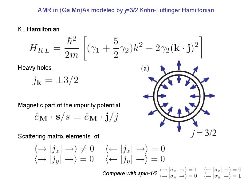
AMR in (Ga, Mn)As modeled by j=3/2 Kohn-Luttinger Hamiltonian KL Hamiltonian Heavy holes Magnetic part of the impurity potential Scattering matrix elements of Compare with spin-1/2

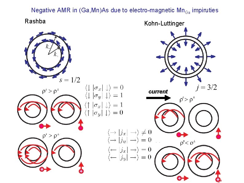
Negative AMR in (Ga, Mn)As due to electro-magnetic Mn. Ga impiruties Rashba Kohn-Luttinger current

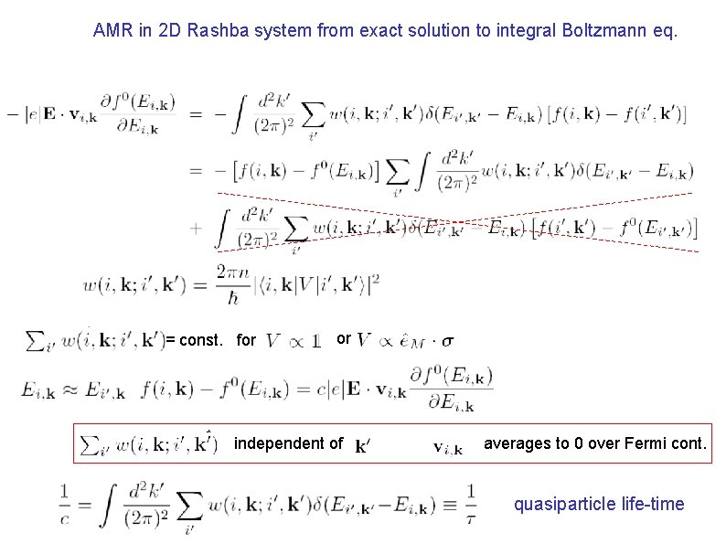
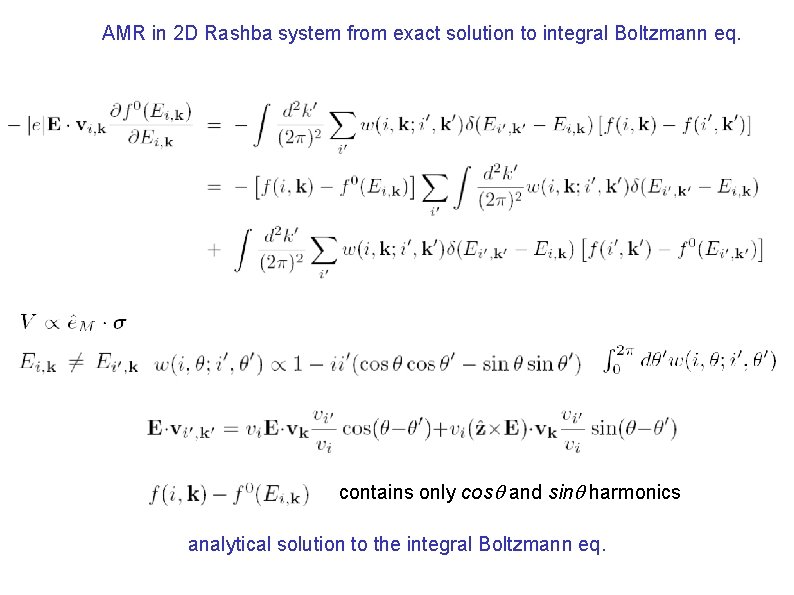
AMR in 2 D Rashba system from exact solution to integral Boltzmann eq. = const. for or independent of averages to 0 over Fermi cont. quasiparticle life-time

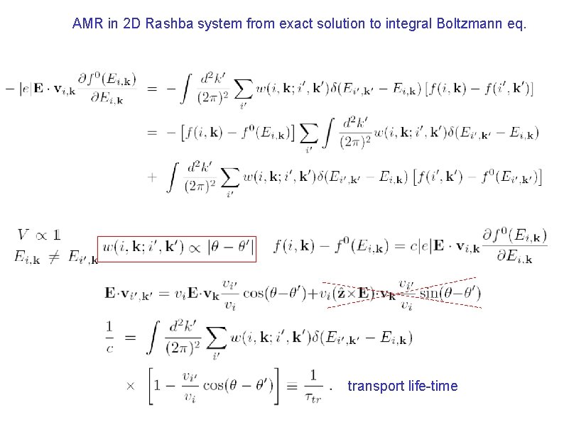
AMR in 2 D Rashba system from exact solution to integral Boltzmann eq. transport life-time

transport life-time is a good first approximation to AMR

AMR in 2 D Rashba system from exact solution to integral Boltzmann eq. contains only cos and sin harmonics analytical solution to the integral Boltzmann eq.

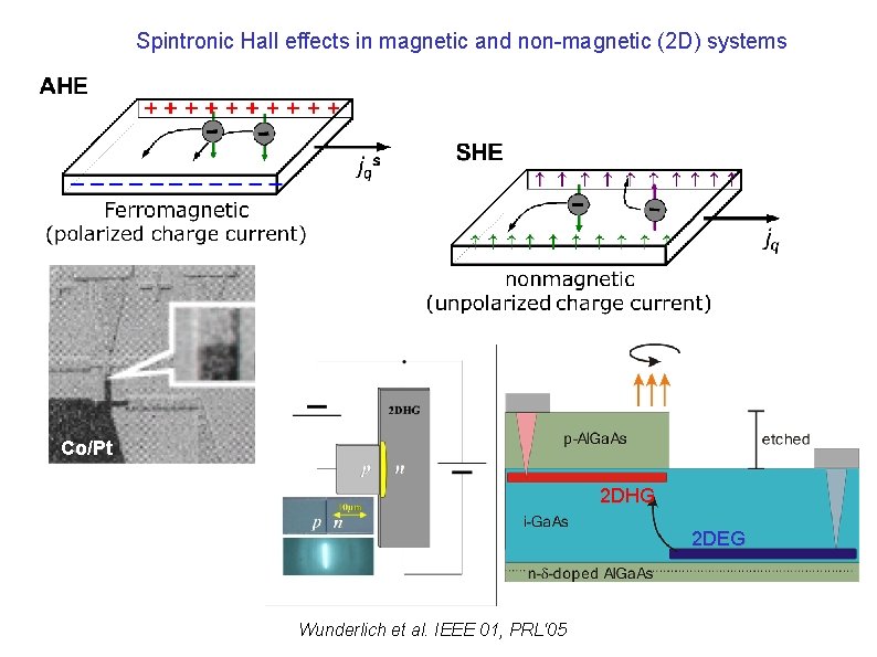
Spintronic Hall effects in magnetic and non-magnetic (2 D) systems Co/Pt 2 DHG 2 DEG Wunderlich et al. IEEE 01, PRL‘ 05

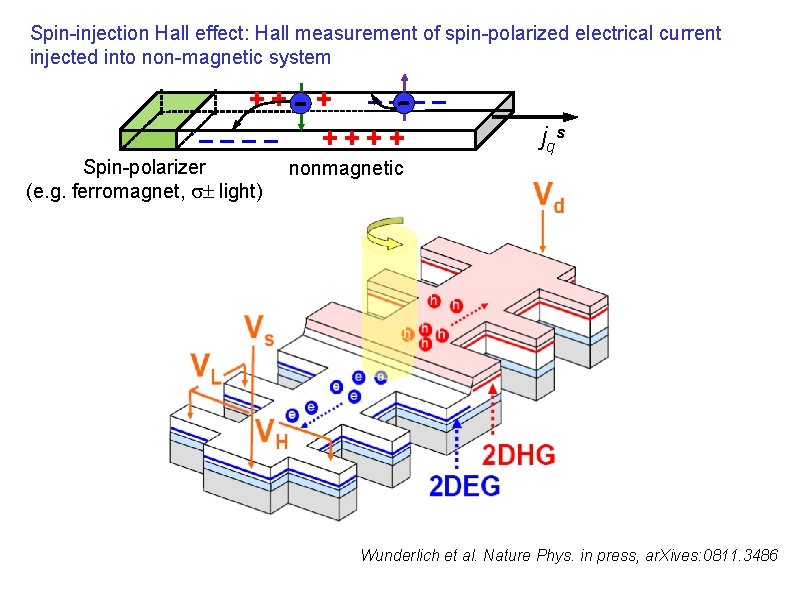
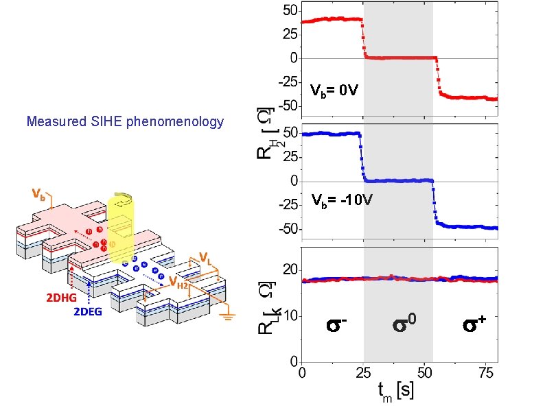
Spin-injection Hall effect: Hall measurement of spin-polarized electrical current injected into non-magnetic system ++++ –––– ++++ Spin-polarizer (e. g. ferromagnet, light) j qs nonmagnetic Wunderlich et al. Nature Phys. in press, ar. Xives: 0811. 3486

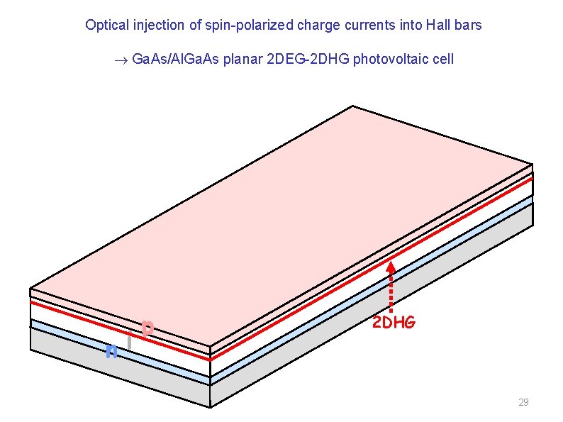
Optical injection of spin-polarized charge currents into Hall bars Ga. As/Al. Ga. As planar 2 DEG-2 DHG photovoltaic cell ni p 2 DHG 29

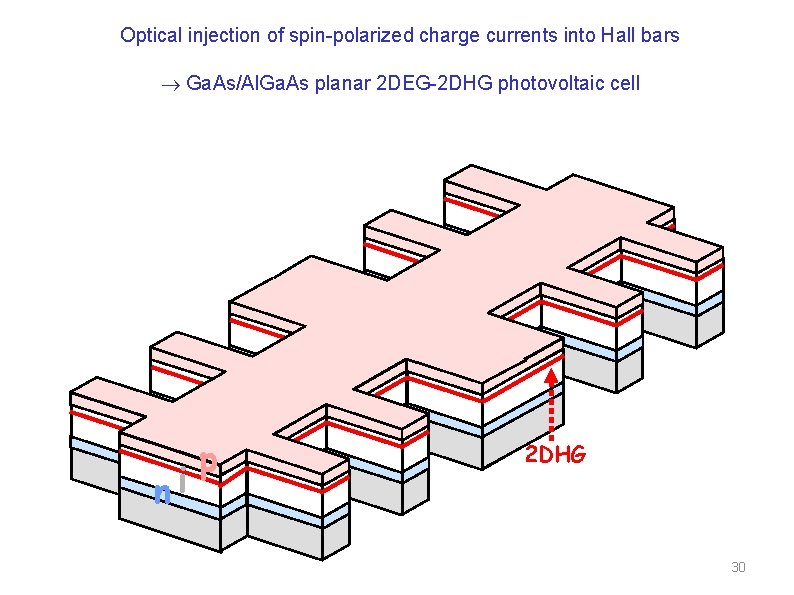
Optical injection of spin-polarized charge currents into Hall bars Ga. As/Al. Ga. As planar 2 DEG-2 DHG photovoltaic cell - ni p 2 DHG 30

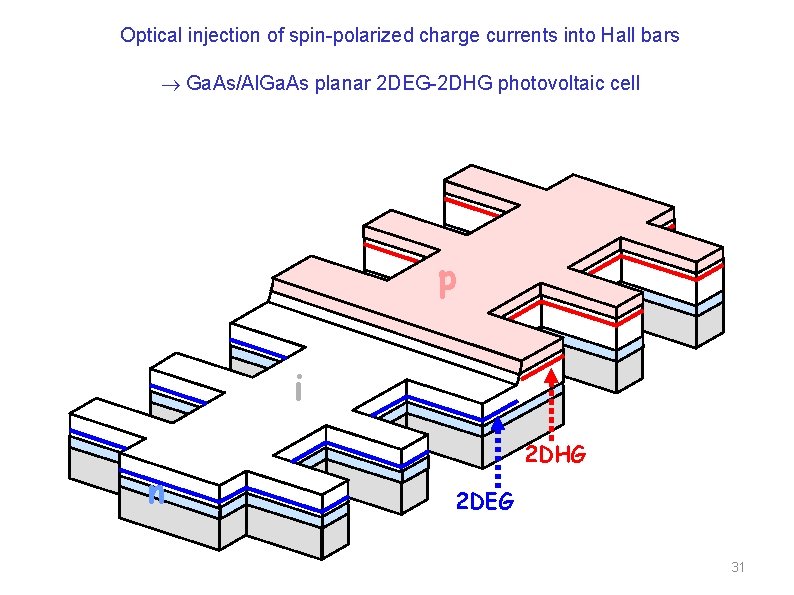
Optical injection of spin-polarized charge currents into Hall bars Ga. As/Al. Ga. As planar 2 DEG-2 DHG photovoltaic cell p i n 2 DHG 2 DEG 31

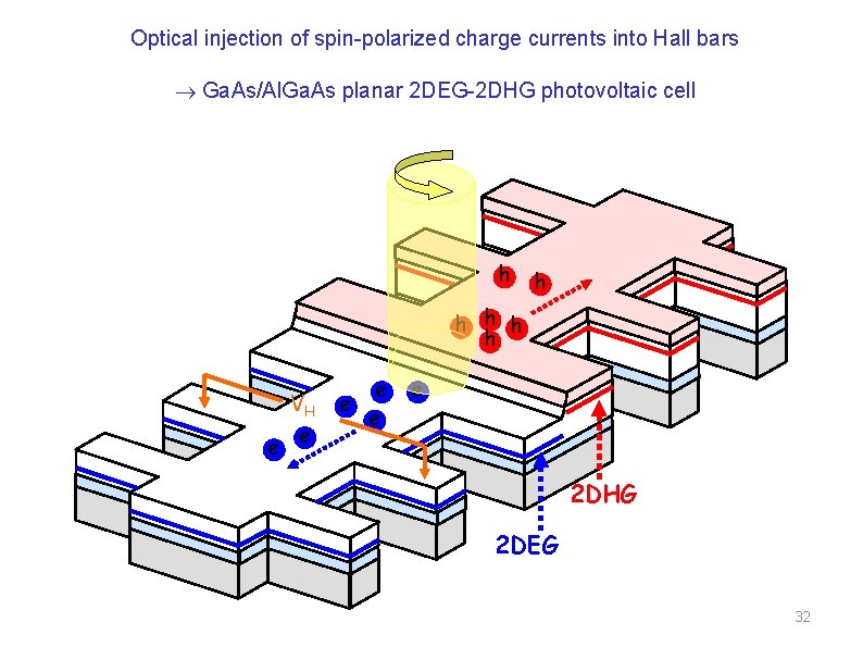
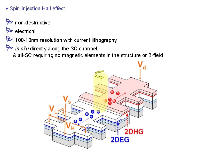
Optical injection of spin-polarized charge currents into Hall bars Ga. As/Al. Ga. As planar 2 DEG-2 DHG photovoltaic cell h h h e VH e e e 2 DHG 2 DEG 32

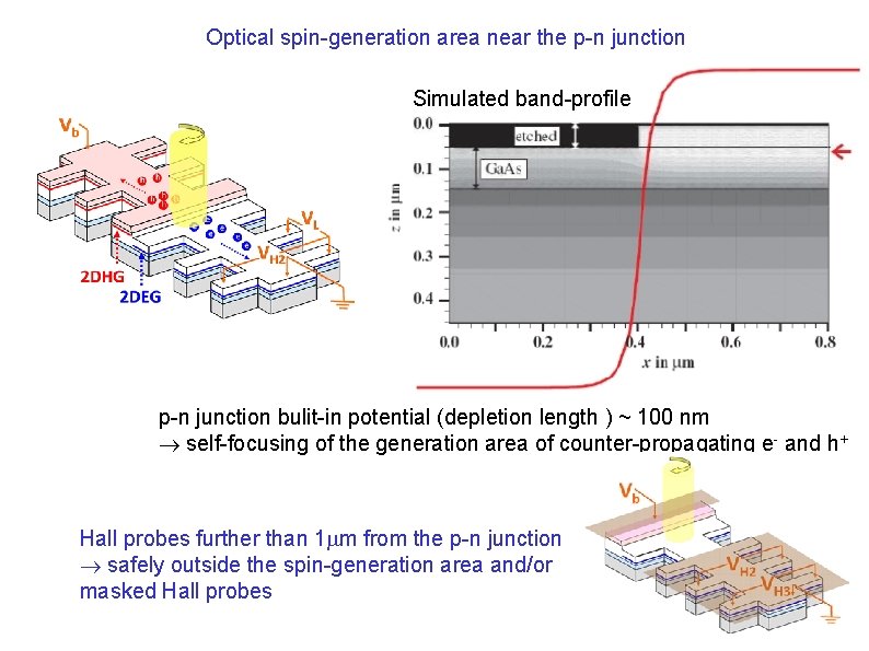
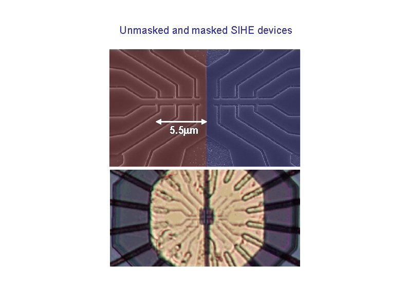
Optical spin-generation area near the p-n junction Simulated band-profile p-n junction bulit-in potential (depletion length ) ~ 100 nm self-focusing of the generation area of counter-propagating e- and h+ Hall probes further than 1 m from the p-n junction safely outside the spin-generation area and/or masked Hall probes

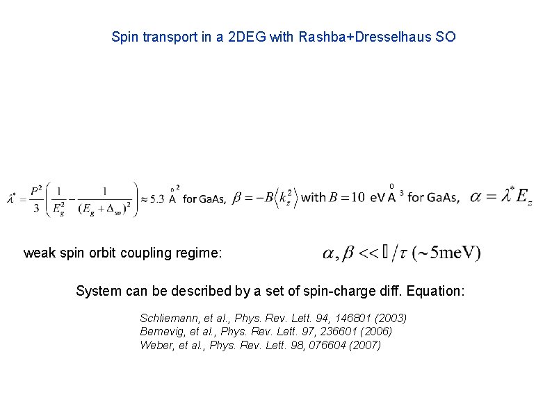
Spin transport in a 2 DEG with Rashba+Dresselhaus SO weak spin orbit coupling regime: System can be described by a set of spin-charge diff. Equation: Schliemann, et al. , Phys. Rev. Lett. 94, 146801 (2003) Bernevig, et al. , Phys. Rev. Lett. 97, 236601 (2006) Weber, et al. , Phys. Rev. Lett. 98, 076604 (2007)

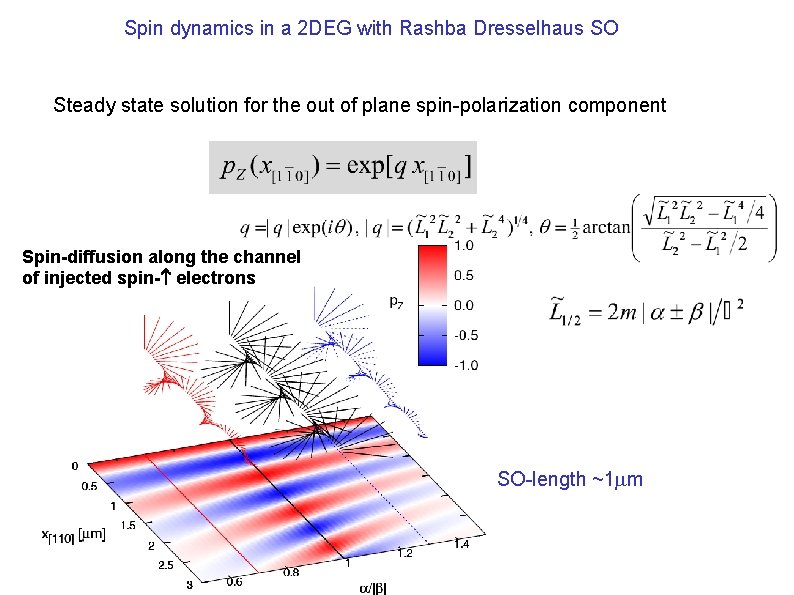
Spin dynamics in a 2 DEG with Rashba Dresselhaus SO Steady state solution for the out of plane spin-polarization component Spin-diffusion along the channel of injected spin- electrons SO-length ~1 m

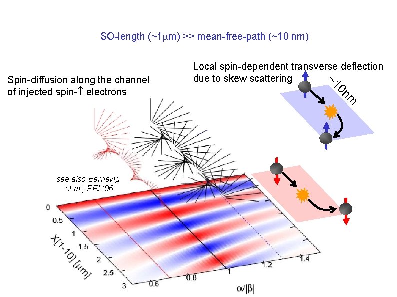
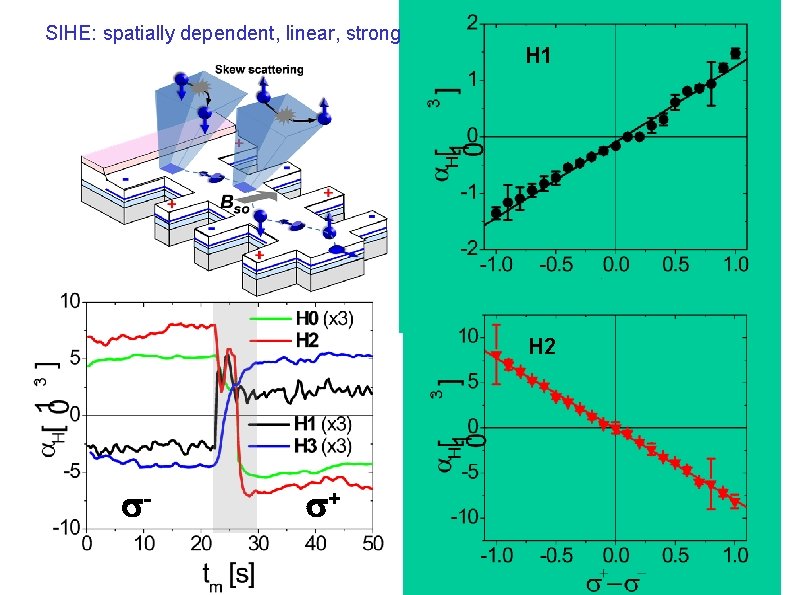
SO-length (~1 m) >> mean-free-path (~10 nm) m 0 n ~1 Spin-diffusion along the channel of injected spin- electrons Local spin-dependent transverse deflection due to skew scattering see also Bernevig et al. , PRL‘ 06

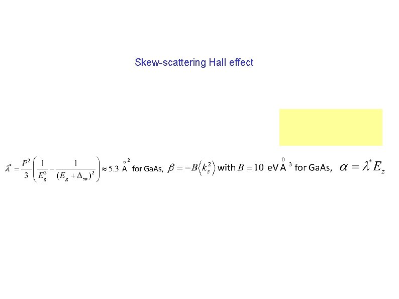
Skew-scattering Hall effect

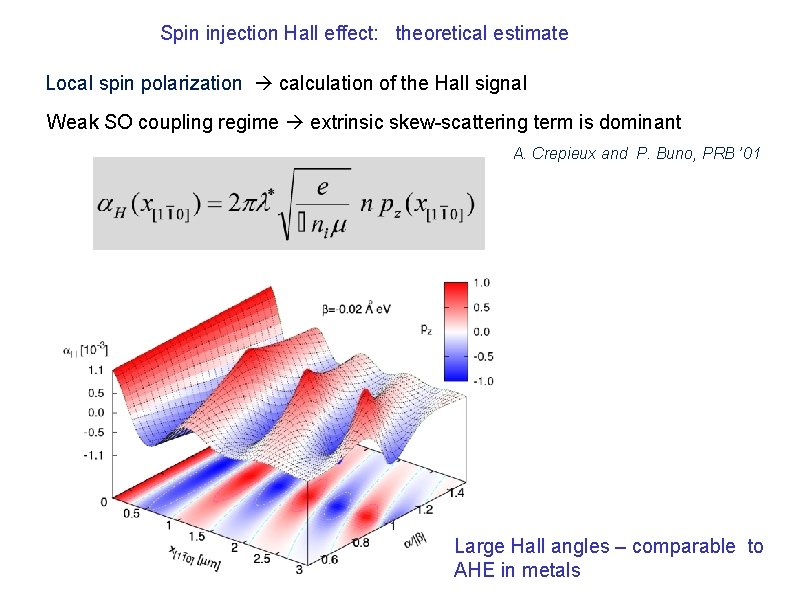
Spin injection Hall effect: theoretical estimate Local spin polarization calculation of the Hall signal Weak SO coupling regime extrinsic skew-scattering term is dominant A. Crepieux and P. Buno, PRB ’ 01 Large Hall angles – comparable to AHE in metals

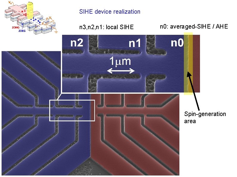
SIHE device realization n 3, n 2, n 1: local SIHE 3 2 1 0 n 0: averaged-SIHE / AHE Spin-generation area

Unmasked and masked SIHE devices 5. 5 m

Vb= 0 V Measured SIHE phenomenology Vb= -10 V - 0 +

SIHE: spatially dependent, linear, strong H 1 H 2 - +

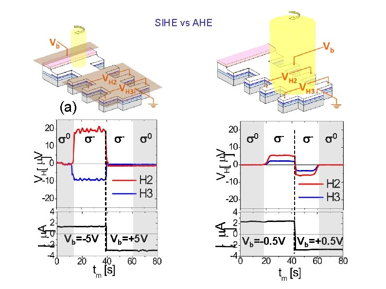
SIHE vs AHE (a) 0 - Vb=-5 V - 0 Vb=+5 V 0 - Vb=-0. 5 V - 0 Vb=+0. 5 V

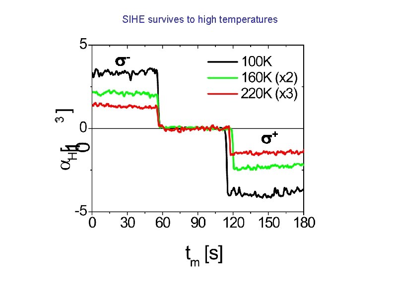
SIHE survives to high temperatures - +

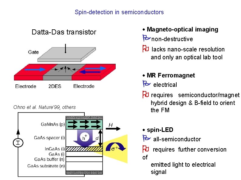
Spin-detection in semiconductors Datta-Das transistor · Magneto-optical imaging non-destructive lacks nano-scale resolution and only an optical lab tool · MR Ferromagnet electrical requires semiconductor/magnet hybrid design & B-field to orient the FM Ohno et al. Nature’ 99, others · spin-LED all-semiconductor requires further conversion of emitted light to electrical signal

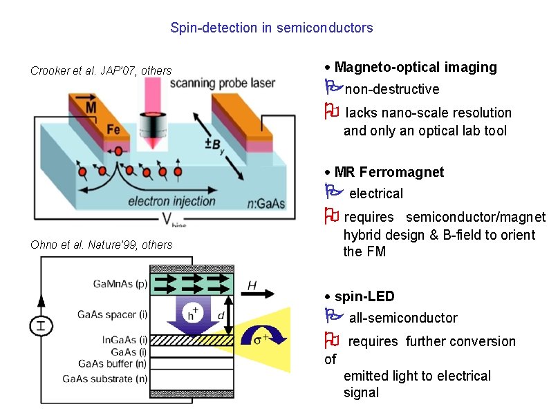
Spin-detection in semiconductors Crooker et al. JAP’ 07, others · Magneto-optical imaging non-destructive lacks nano-scale resolution and only an optical lab tool · MR Ferromagnet electrical requires semiconductor/magnet hybrid design & B-field to orient the FM Ohno et al. Nature’ 99, others · spin-LED all-semiconductor requires further conversion of emitted light to electrical signal

· Spin-injection Hall effect non-destructive electrical 100 -10 nm resolution with current lithography in situ directly along the SC channel & all-SC requiring no magnetic elements in the structure or B-field

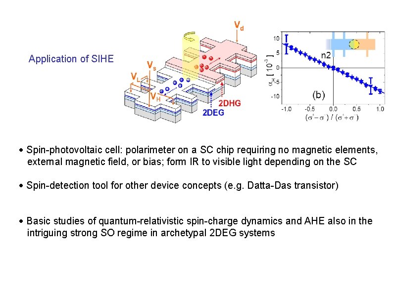
Application of SIHE · Spin-photovoltaic cell: polarimeter on a SC chip requiring no magnetic elements, external magnetic field, or bias; form IR to visible light depending on the SC · Spin-detection tool for other device concepts (e. g. Datta-Das transistor) · Basic studies of quantum-relativistic spin-charge dynamics and AHE also in the intriguing strong SO regime in archetypal 2 DEG systems
