Spintronics starting with Giant Magneto Resistance GMR Basics
")
Spintronics – starting with Giant Magneto. Resistance (GMR)
 in a ferromagnet")
Basics electrical conduction in a ferromagnet The density of states (DOS) in a ferromagnet is split into majority and minority bands due to the exchange interaction n(E) majority 3 d EF 4 s E minority q s- and d-electrons contribute to electrical conduction, BUT the mobility of 3 d-electrons is smaller (flat energy bands → low velocity/high effective mass) than for 4 s-electrons. Only electron-states close to the Fermi energy are of importance. q In the example above, ↓-electrons have more empty states to scatter to, the resistivity will be higher for these electrons, , two independent parallel electron conduction channels. q Neglecting sd, the resistivity of ↑-electrons (majority electrons) will be , while the resistivity of ↓-electrons (minority electrons) can be written as , since many empty 3 d states imply large scattering cross-section.
 and")
GMR Spin dependent scattering, two current channels, one for majority spins (low resistivity) and one for minority spins (high resistivity) System geometries displaying GMR CIP (Current In Plane) multilayers CPP (Current Perpendicular Plane) multilayers E, J FM e- FM Me Me FM FM H FM = metallic ferromagnetic layer; Me = metallic non-magnetic layer E, J
n multilayers FM = Fe, Ni, Co or")
(FM t. FM / Me t. Me)n multilayers FM = Fe, Ni, Co or 3 d alloy, Me = Cu, Ag, V, Cr, t. FM (Me) = layer thickness ≈ a few monolayers (some nm thickness) High resistance for antiferromagnetically (AF) aligned layers, low resistance for ferromagnetically (F) aligned layers. CIP geometry HS The microscopic origin of the AF coupling is explained by the RKKY (Ruderman-Kittel-Kasuya -Yosida) model, indirect type of interaction between two FM layers, FM 1 polarizes the conduction electron spins and the spin polarization propagates across the Me spacer layer and interacts with FM 2, spin polarization oscillates in sign and decays with distance as r-2

FM 1 Me FM 2 M F coupling AF coupling H

Mechanism of GMR Two current channels with different resistivities, the difference is explained by the electronic structure and differences in the DOS for the majority and minority conduction electrons. In addition, we need to consider scattering centres, here we distinguish between bulk scattering and interface (FM/Me) e. FM elements interface bulk FM alloys Two prerequisites for scattering/resistance; i) empty states at EF ii)scattering centres Scattering centres at interfaces may be surface roughness, regions of interdiffusion, etc. , while scattering in the bulk of a layer is due to impurity atoms.

Important length scales; spin diffusion length lsdl , should be , lsdl ~ 102 – 103 nm for magnetic 3 d elements; mean free path lmfp , should be , lmfp ~ 10 – 30 nm for magnetic 3 d elements and only a few nm for alloys like permalloy. If these conditions hold, one would expect similar results for the CIP and CPP geometries. The resistance of the different current channels can be described using simple resistor models. AF configuration where R+ (R_ ) is the resistance for electrons with S=+1/2 (S= ‒ 1/2 ), while are the resistances for the two conduction channels (minority and majority carriers, respectively). F configuration
")
The magnetoresistance thus is In the absence of AF coupling, there are (at least) two possible ways to obtain opposite orientation of the magnetizations in neighboring FM layers in a field interval: I. Use two ferromagnetic materials exhibiting different coercivities, either as building block in a multilayer or as part of a sandwich structure. II. Use two FM layers separated by a Me layer in a sandwhich structure, one FM layer will be constrained by coupling to an adjacent antiferromagnetic layer (exchange anisotropy); Fe. Mn (TN ≈ 430 K), Ir. Mn (TN ≈ 470 K), . . . FM 1 Me FM 2 AF uni-directional anisotropy!

How to prepare the layer so that it exhibits exchange anisotropy TN = Néel temperature, ordering temperature for the antiferromagnetic layer

Si /(60 Å Ni 80 Fe 20 / 22 Å Cu / 40 Å Ni 80 Fe 20 / 70 Å Fe. Mn) / 50 Å Ta) Multilayered or sandwich structures in applications? Multilayer Sandwich

SPINTRONICS The acronym was originally used as the name for a research program at DARPA (Defence Advanced Research Project Agency) Overall goals I. To produce a new generation of electronic devices where the spin of the carriers should play a crucial role in addition to or in place of the charge II. To produce such materials that can be integrated with existing semiconductor materials One example Magnetoresistive Random Access Memory – MRAM

q IBM – Infineon in 2005 demonstrated a 16 -Mbit magnetoresistive random access memory (MRAM) prototype q Freescale Semiconductor Inc. summer 2006 introduced its first 4 -Mbit MRAM product Magnetic tunnel junctions Quantum mechanics dictates that an electron in a metallic electrode has a certain probability to tunnel through an (insulating) potential barrier to another metallic electrode. Important parameters – thickness of barrier, height of potential barrier and density of states (DOS) in the metallic electrodes, . In ferromagnets like Fe, Ni and Co, the DOS for spin-up and spin-down 3 d electrons are exchange split.

Tunnelling between two ferromagnetic electrodes electrode 1 barrier electrode 2 half-metallic parallel alignment assumptions electrons keep their 3 dcharacter and spin during tunnelling half-metallic → spin dependent transport, important parameter – spin polarization antiparallel alignment
) FM 1 spin conservation")
Jullière’s model (M. Julliere, Physics Letters 54 A, 225 (1975)) FM 1 spin conservation the conductance is proportional to products like insulator FM 2 Relation between conductivity and resistivity changes ( conductivity (resistivity) for parallel magnetizations …) Conductance when the magnetizations in the two FM electrodes are parallel ( Fermi-Dirac distribution) and the corresponding result when the electrode magnetizations are in opposite directions

Using the definition of spin polarization, we obtain and can be generalized to two different FM materials with two different spin polarizations; P 1 and P 2 Theory by Slonczewski (Phys. Rev. B 39, 6995 (1989)) describes how the tunneling conductance depends on barrier height. Typical dimensions FM electrodes sub-mm in size, thickness 10 -20 nm Oxide tunnel barrier one or a few nm thick, barrier height 2 -3 e. V (~band-gap) Materials FM electrodes Co, Fe, Ni. Fe, Co. Fe. B Amorphous oxide tunnel barrier Ni. O, Co. O, Al 2 O 3, or crystalline tunneling barrier Mg. O Junction resistance from < 100 W to tens of k. W, depends exponentially on barrier thickness
 interdiffusion, minimum of spin-flip scattering at")
Important Sharp interfaces without (as far as possible) interdiffusion, minimum of spin-flip scattering at interfaces Measured spin polarizations P (Meservey and Tedrow, Phys. Rep. 238, 173 (1994)) Material Ni Co Fe Ni. Fe Co. Fe P +23% +35% +40 +32% ~50% How to prepare a junction in low / high resistance states M -H 3 -H 2 H 1 R -H 3 -H 2 H 1 one FM electrode may be pinned by an AF layer or the FM layers may have different Hci (in graph we assume different Hci) Non-volatile memory!

TMR-results for Co/Al 2 O 3/Ni. Fe junctions 20. 2% RT 27. 1% 77 K 27. 3% 4. 2 K

‘Recent’ advances – epitaxial barriers or barriers with texture First-principles based calculations of the tunneling conductance in Fe(001) | Mg. O(001) | Fe(001) junctions, W. H. Butler et al. , Phys. Rev. B 63, 054416 (2001) Experimental confirmation Stuart S. P. Parkin et al, Nature Materials 3, 862 (2004); Shinji Yuasa et al, Nature Materials 3, 868 (2004) Good results both for epitaxial junctions and polycrystalline but highly (001) oriented junctions.

Fe | Mg. O | Fe | Ir. Mn epitaxial junctions at 293 K and at 20 K.

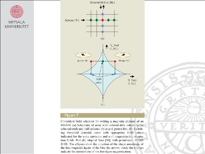
q Writing by currents in one word and one bit line (the total field is large enough to switch the magnetization in one electrode) q Reading by probing the resistance over one TMR junction

Different Hci Exchange bias II

Comparison of memory technologies CMOS Technology DRAM SRAM Flash MRAM Bit Cell Area (F 2) ~ 100 ~ 10 Read / Write Cycle (65 nm) 4 ns / 4 ns 1 ns / 1 ns 10 ns / 100 ns 2 ns / 2 ns Endurance cycles Infinite 105 Infinite Non-volatile No No Yes Low voltage Limited Yes Future scalability Limited Good
 Spin torque transfer switching Manipulation")
2007 R&D moving to spin transfer torque RAM (SPRAM) Spin torque transfer switching Manipulation of magnetic moments in a nano-scale ferromagnet by a current is one of the most important techniques for the future spintronics devices. Especially, current induced magnetization switching in magnetic tunnel junctions (MTJs) is expected to be the method for writing in high density magnetoresistive random access memory (MRAM). The necessary critical current for spin transfer switching decreases as l 2 (where l is the in-plane dimension of the TMR structure) as the free-layer volume decreases. From this scalability, the spin transfer torque switching can reduce the writing current in MRAM and avoid excessive heating, while the conventional writing method using the magnetic field generated by currents needs larger writing current. The spin torque transfer switching will allow for higher density MRAM memory units. Switching current (*): a = magnetic damping constant; Ha = anisotropy field; V = volume of ’free’ layer; Eb = energy barrier; g = function of spin polarization of tunnel current and angle between magnetization of free and pinned layers * J. Slonczewski, JMMM 159, L 1 -7 (1996); L. Berger, PRB 54, 9353 -9358 (1996)

Electrons flowing through a magnetic layer in a magnetoresistive device are spin polarized along the magnetization of F 1. Fig. 1 Schematic illustration of spin torque transfer When these spin-polarized electrons pass through another magnetic layer (F 2), the polarization direction will change depending on the relative orientation of F 1 and F 2. In this repolarization process, F 2 experiences a torque (spin torque) associated with the transfer of spin angular momentum from the electrons. For large current, the spin torque amplifies the spin precession and magnetization switching occurs. The magnetization of the free layer is controlled by the current direction. Fig. 2 Typical TMR loop driven by a pulse current.
 -")
Some recent news 2007 - R&D moving to spin transfer torque RAM (SPRAM) - February – Tohoku University and Hitachi developed a prototype 2 Mbit Non-Volatile RAM Chip employing spin-transfer torque switching - August – IBM, TDK Partner In Magnetic Memory Research on Spin Transfer Torque Switching to lower the cost and boost performance of MRAM - November – Toshiba applied and proved the spin transfer torque switching with perpendicular magnetic anisotropy MTJ device - November – NEC Develops World's Fastest SRAM-Compatible MRAM With Operation Speed of 250 MHz 2009 - January – Japanese satellite, Sprite Sat, uses a MRAM from Everspin Technologies (former Freescale), used as backup-memory in the control unit for the navigation system - June – Hitachi and Tohoku University demonstrated a 32 -Mbit spin-transfer torque MRAM - August – Scientists in Germany have developed next-generation MRAM that is said to operate as fast as fundamental performance limits allow, with write cycles below 1 nanosecond. 2010 - A perpendicular-anisotropy Co. Fe. B-Mg. O magnetic tunnel junction S. Ikeda et al. , Nature Materials 9, 721 -724 (2010) 2011 - March – PTB, Germany, announces having achieved a below 500 ps (2 GBit/s) write cycle[24] 2012 -November –Everspin Technologies introduces the first 64 Mb ST-MRAM. The device is the first product in Everspin’s ST-MRAM roadmap that is planned to scale to gigabit density memories with faster speeds. 2013 - November, Buffalo Technology and Everspin announce a new industrial SATA III SSD that incorporates Everspin’s Spin-Torque MRAM as cache memory.

40 nm TMR device low switching current < Ic > = 50 m. A; 120% TMR ratio; high thermal stabilty factor Eb / k. BT = 43

Mål • Känna till att det finns 2 strömkanaler för ledningselektroner i ett metalliskt ferromagnetiskt material, en kanal för majoritetselektroner och en annan för minoritetselektroner • Känna till hur ett magnetiskt multilager som uppvisar GMR effekten är uppbyggt och de magnetiska tillstånden (hur magnetiseringen i olika skikt är riktade) för hög respektive låg resistans • Kunna förklara GMR effekten m. h. a. strömkanalerna för majoritets- och minoritetselektroner • Känna till vad som menas med ”exchange anisotropy” • Känna till hur magnetiska tunnelövergångar är uppbyggda och kvalitativt kunna redogöra för tunnelmagnetoresistans (TMR) m. h. a. DOS för majoritets– och minoritetselektronerna • Kunna beskriva hur resistansen för ett TMR element varierar med magnetiseringen för elementet. Hur ”sätter” man elementet i ett högresistanstillstånd? • Känna till tunnelövergångar som utnyttjar Mg. O barriären • Kunna beskriva utformningen av ett MRAM med ”bit” och ”word” ledare • Kvalitativt kunna beskriva hur man byter riktning på det fria lagrets magnetisering om man använder en spinnpolariserad ström i ett TMR element
- Slides: 28