An Integrated ECC and Redundancy Repair Scheme for

- Slides: 16

An Integrated ECC and Redundancy Repair Scheme for Memory Reliability Enhancement Chin-Lung Su, Yi-Ting Yeh, and Cheng-Wen Wu National Tsing Hua University Hsinchu, Taiwan

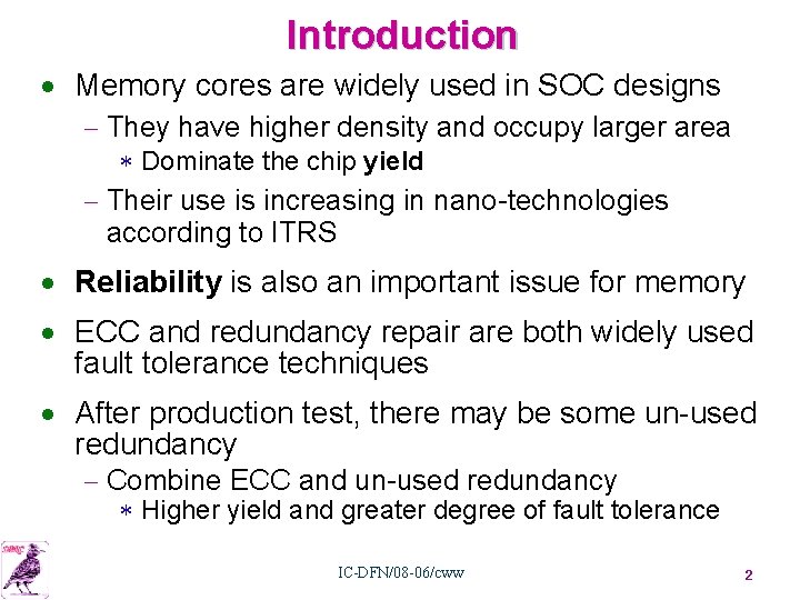
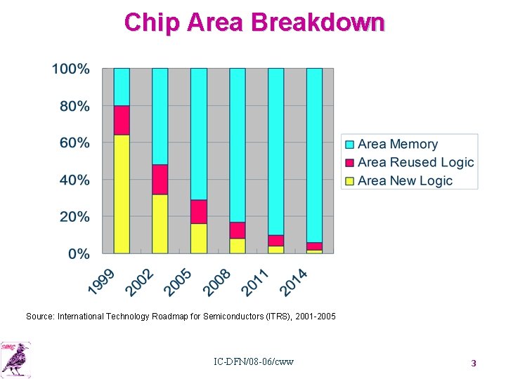
Introduction · Memory cores are widely used in SOC designs - They have higher density and occupy larger area * Dominate the chip yield - Their use is increasing in nano-technologies according to ITRS · Reliability is also an important issue for memory · ECC and redundancy repair are both widely used fault tolerance techniques · After production test, there may be some un-used redundancy - Combine ECC and un-used redundancy * Higher yield and greater degree of fault tolerance IC-DFN/08 -06/cww 2

Chip Area Breakdown Source: International Technology Roadmap for Semiconductors (ITRS), 2001 -2005 IC-DFN/08 -06/cww 3

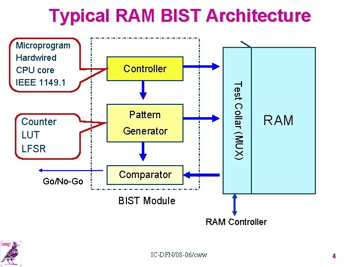
Typical RAM BIST Architecture Counter LUT LFSR Go/No-Go Controller Test Collar (MUX) Microprogram Hardwired CPU core IEEE 1149. 1 Pattern Generator RAM Comparator BIST Module RAM Controller IC-DFN/08 -06/cww 4

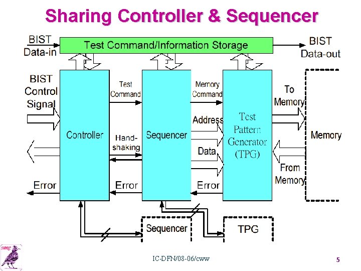
Sharing Controller & Sequencer IC-DFN/08 -06/cww 5

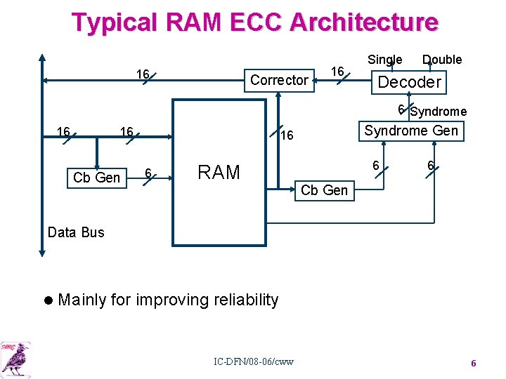
Typical RAM ECC Architecture 16 Corrector 16 Single Double Decoder 6 Syndrome 16 16 Cb Gen Syndrome Gen 16 6 RAM 6 6 Cb Gen Data Bus l Mainly for improving reliability IC-DFN/08 -06/cww 6

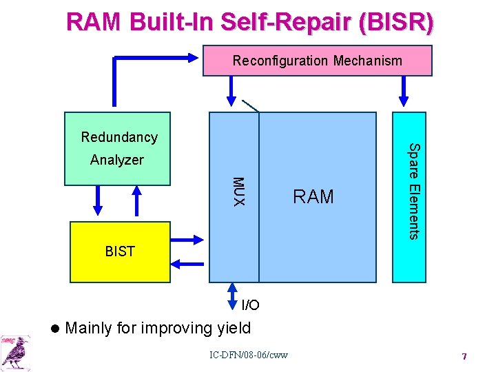
RAM Built-In Self-Repair (BISR) Reconfiguration Mechanism Analyzer MUX RAM Spare Elements Redundancy BIST I/O l Mainly for improving yield IC-DFN/08 -06/cww 7

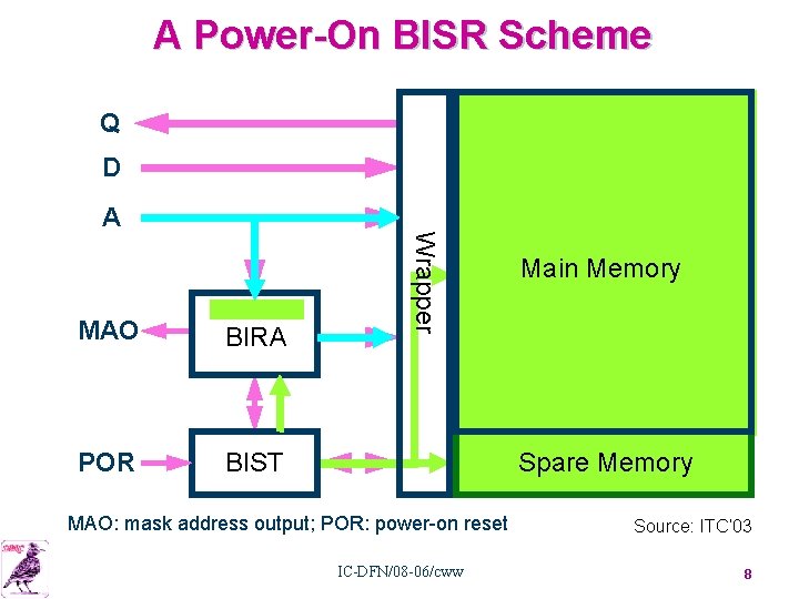
A Power-On BISR Scheme Q D MAO BIRA POR BIST Wrapper A Main Memory Spare Memory MAO: mask address output; POR: power-on reset IC-DFN/08 -06/cww Source: ITC’ 03 8

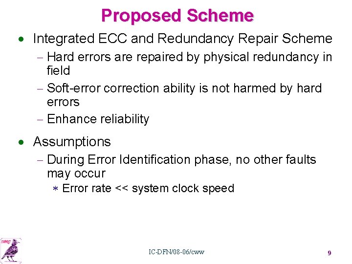
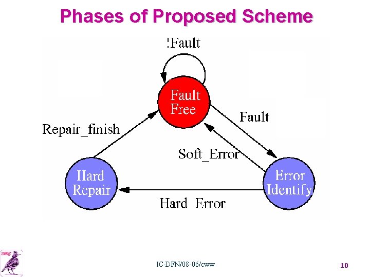
Proposed Scheme · Integrated ECC and Redundancy Repair Scheme - Hard errors are repaired by physical redundancy in field - Soft-error correction ability is not harmed by hard errors - Enhance reliability · Assumptions - During Error Identification phase, no other faults may occur * Error rate << system clock speed IC-DFN/08 -06/cww 9

Phases of Proposed Scheme IC-DFN/08 -06/cww 10

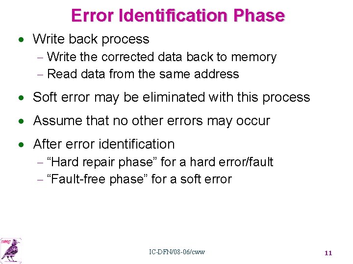
Error Identification Phase · Write back process - Write the corrected data back to memory - Read data from the same address · Soft error may be eliminated with this process · Assume that no other errors may occur · After error identification - “Hard repair phase” for a hard error/fault - “Fault-free phase” for a soft error IC-DFN/08 -06/cww 11

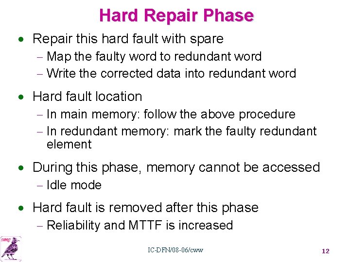
Hard Repair Phase · Repair this hard fault with spare - Map the faulty word to redundant word - Write the corrected data into redundant word · Hard fault location - In main memory: follow the above procedure - In redundant memory: mark the faulty redundant element · During this phase, memory cannot be accessed - Idle mode · Hard fault is removed after this phase - Reliability and MTTF is increased IC-DFN/08 -06/cww 12

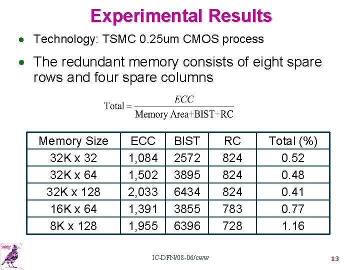
Experimental Results · Technology: TSMC 0. 25 um CMOS process · The redundant memory consists of eight spare rows and four spare columns Memory Size 32 K x 32 32 K x 64 32 K x 128 16 K x 64 8 K x 128 ECC 1, 084 1, 502 2, 033 1, 391 1, 955 BIST 2572 3895 6434 3855 6396 IC-DFN/08 -06/cww RC 824 824 783 728 Total (%) 0. 52 0. 48 0. 41 0. 77 1. 16 13

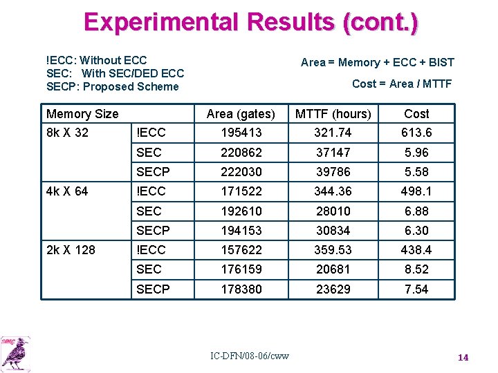
Experimental Results (cont. ) !ECC: Without ECC SEC: With SEC/DED ECC SECP: Proposed Scheme Memory Size 8 k X 32 4 k X 64 2 k X 128 Area = Memory + ECC + BIST Cost = Area / MTTF Area (gates) MTTF (hours) Cost !ECC 195413 321. 74 613. 6 SEC 220862 37147 5. 96 SECP 222030 39786 5. 58 !ECC 171522 344. 36 498. 1 SEC 192610 28010 6. 88 SECP 194153 30834 6. 30 !ECC 157622 359. 53 438. 4 SEC 176159 20681 8. 52 SECP 178380 23629 7. 54 IC-DFN/08 -06/cww 14

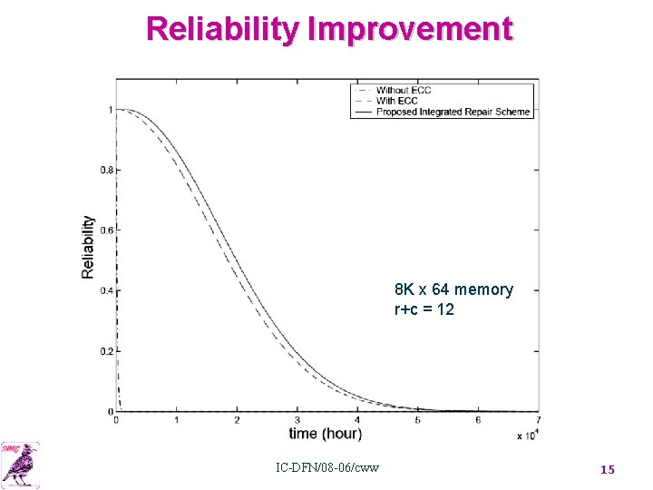
Reliability Improvement 8 K x 64 memory r+c = 12 IC-DFN/08 -06/cww 15

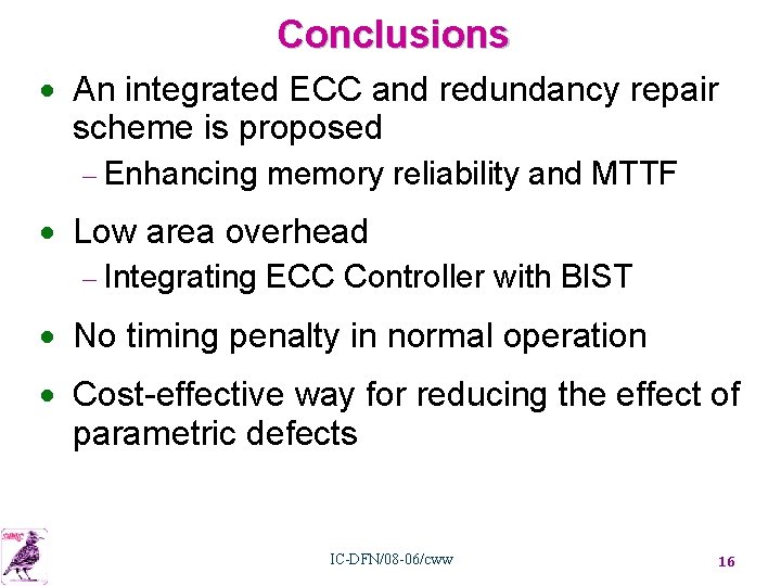
Conclusions · An integrated ECC and redundancy repair scheme is proposed - Enhancing memory reliability and MTTF · Low area overhead - Integrating ECC Controller with BIST · No timing penalty in normal operation · Cost-effective way for reducing the effect of parametric defects IC-DFN/08 -06/cww 16