A conductoris a material which permits a flow


 is the energy of the highest occupied state.")
")


 is a technique for determining the arrangement of atoms")
. The Bragg equation n λ = 2 d sin")

- Slides: 32
A conductoris a material which permits a flow of energy. A material which allows the flow of charged particles is an electrical conductor. A material which allows the transfer of thermal energy is a thermal conductor or heat conductor. Insulators: An insulator is a material such as plastic, rubber, glass or ceramic that prevents the flow or transfer of electricity. Insulative materials can not be grounded. Attaching a ground wire to an insulator would have no effect. A material that is neither a good conductor of electricity (like copper) nor a good insulator (like rubber). The most common semiconductor materials are silicon and germanium. These materials are then doped to create an excess or lack of electrons.
semiconductor, solid material whose electrical conductivity at room temperature is between that of a conductor and that of an insulator. At high temperatures its conductivity approaches that of a metal, and at low temperatures it acts as an insulator. In a semiconductor there is a limited movement of electrons, depending upon the crystal structure of the material used. The substances first used for semiconductors were the elements germanium, silicon, and gray tin. It was found that the incorporation of certain impurities in them enhances their conductive properties. The impurities either add free electrons or create holes (electron deficiencies) in the crystal structures of the host substances by attracting electrons. Thus there are two types of semiconductor: the Ntype (negative), in which the current carriers (electrons) are negative, and the P-type (positive), in which the positively charged holes move and carry the current. The process of adding these impurities is called doping; the impurities themselves are called dopants. Dopants that contribute mobile electrons are called donor impurities; those that cause holes to form are acceptor impurities. Undoped semiconductor material is called intrinsic semiconductor material. Certain chemical compounds, including gallium arsenide, indium antimonide, and aluminum phosphide are semiconductors. Semiconductors are used to produce such electronic devices as diodes, transistors, and computer memory devices. The field of solid-state physics includes the study of semiconductors.
n-typesemiconductors result from the addition of pentavalent impurities like phosphorus, arsenic and antimony. These donors contribute “extra” electrons. p-typesemiconductors result from the addition of trivalent impurities like boron, aluminum and gallium. These additions create valence “holes” which act as additional levels
Figure 13. 29: Effect of doping silicon. 5
Figure 13. 30: A p-n junction as a rectifier. 6
Insulators: Valence band full or nearly full Wide band gap with empty conduction band Essentially no available energy states to which electron energies can be increased Conduction band Empty Eg Wide bandgap Valence band Full Dielectric breakdown at high potential
Semiconductors: Similar to insulators but narrow band gap At electrical temperatures some electrons can be promoted to the conduction band Most are cubic Diamond FCC (single element) Zinc blende (FCC Zn. S) Conduction band Almost Empty Eg Conduction band Empty bandgap Valence band Almost Full Valence band Full T = 0 K T > 0 K Some common band gaps: Element gap (ev) Ge 0. 6 Si 1. 1 Ga. As 1. 4 Si. O 2 9. 0 Mark Mc. Clure, UNCPembroke S Zn
Band Theory As the half-filled 4 s orbitals of an increasing number of Cu atoms overlap, their energies are split into a halffilled valence band. Electrons can move from the filled half (purple) to the slightly higher energy upper half (red), where they are free to migrate from one empty orbital to another.
Metallic Bonds Band theory is an extension of molecular orbital theory that describes bonding in solids. Bands of orbitals that are filled or partially filled by valence electrons are called valence bands. Higher-energy unoccupied bands in which electrons are free to migrate are called conduction bands.
Band Theory The Band Gap influences the electrical and optical properties of the material. Semiconductor “doping” can be used to create solar cell (PV), diodes, transistors, etc.
Band Theory The Fermi Energy (Level) is the energy of the highest occupied state.
Some semiconducting materials and ssociated bandgaps (e. V)
Other Ionic Crystals
Other forms of Silica
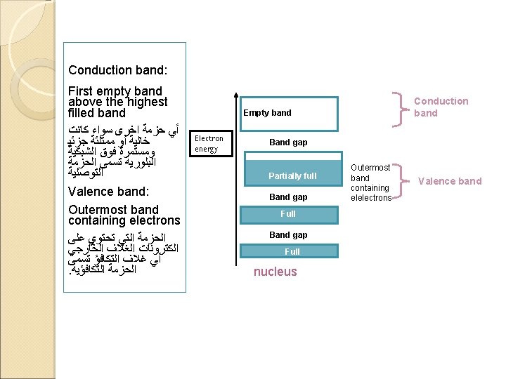
Band Theory of Solids In isolated atoms the electrons are arranged in energy levels
In solids the outer electron energy levels become smeared out to form bands The highest occupied band is called the VALENCE band. This is full. For conduction of electrical energy there must be electrons in the CONDUCTION band. Electrons are free to move in this band.
Insulators : There is a big energy gap between the valence and conduction band. Examples are plastics, paper …. . Conductors : There is an overlap between the valence and conduction band hence electrons are free to move about. Examples are copper, lead …. Semiconductors : There is a small energy gap between the two bands. Thermal excitation is sufficient to move electrons from the valence to conduction band. Examples are silicon , germanium….
When a conductor is heated its resistance increases ; The atoms vibrate more and the electrons find it more difficult to move through the conductor. But in a semiconductor the resistance decreases with an increase in temperature. Electrons can be excited up to the conduction band. Conductivity increases R R T T
Band Theory When two atomic orbitals combine they produce both a bonding and an antibonding molecular orbital • When many atomic orbitals combine they produce a band of bonding molecular orbitals and a band of antibonding molecular orbitals • The band of bonding molecular orbitals is called the valence band • The band of antibonding molecular orbitals is called the conduction band • Tro: Chemistry: A Molecular Approach, 2/e 25
Solids: Conductors, Insulators and Semiconductors Conduction Band: white Band gap No gap Valence Band in red Conductor Insulator Semiconductor 26
Electrical conductivity in a conductor, semiconductor, and insulator. conductor insulator semiconductor
Types of Band Gaps and Conductivity Tro: Chemistry: A Molecular Approach, 2/e 28
Band Gap and Conductivity The more electrons at any one time that a substance has in the conduction band, the better conductor of electricity it is If the band gap is ~0, then the electrons will be almost as likely to be in the conduction band as the valence band the material will be a conductor ◦ metals ◦ the conductivity of a metal decreases with temperature If the band gap is small, then a significant number of the electrons will be in the conduction band at normal temperatures and the material will be a semiconductor ◦ graphite ◦ the conductivity of a semiconductor increases with temperature If the band gap is large, then effectively no electrons will be in the conduction band at normal temperatures and the material will be an insulator Tro: Chemistry: A Molecular Approach, 2/e 29
X-ray Diffraction X-ray diffraction (XRD) is a technique for determining the arrangement of atoms or ion in a crystal by analyzing the pattern that results when X-rays are scattered after bombarding the crystal. The Bragg equation relates the angle of diffraction (2 ) of X-rays to the spacing (d) between the layers of ions or atoms in a crystal: n 2 dsin.
Structure Determination X-ray Diffraction (XRD). The Bragg equation n λ = 2 d sin θ Can be used in conjunction with XRD data to find the spacing between crystal planes (d). l is the wavelength of the X-rays; n is an integer; d is the distance between crystal planes; θ is the angle of incidence.
Peaks result from constructive interference for the reflected X-rays Fig. 10. 3 c: This is an example of an XRD spectrum for quartz.