A 24 GHz Low Noise Amplifier Design Construction
- Slides: 18

A 24 GHz Low Noise Amplifier: Design, Construction, and Testing An Undergraduate Senior Design Project Jeff Keyzer Tony Long

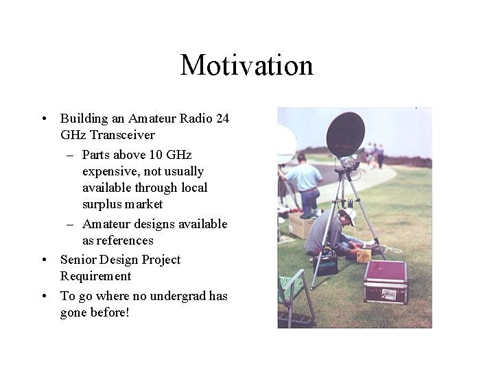
Motivation • Building an Amateur Radio 24 GHz Transceiver – Parts above 10 GHz expensive, not usually available through local surplus market – Amateur designs available as references • Senior Design Project Requirement • To go where no undergrad has gone before!

Design Requirements • > 12 d. B Gain • 2. 0 - 2. 5 d. B Noise Figure – Overcome noisy/lossy 1 st mixer • For passive mixer, Tsys drops from 7402 K to 464 K • For active mixer, Tsys drops from 5612 K to 393 K • Maximum of two stages • Ease of construction - packaged parts a must!!

Our Design Tools • Guillermo Gonzalez, Microwave Transistor Amplifiers (Simon & Schuster 1997) – LNA is based on a very simple “by the book” design. • Amateur Radio Microwave Enthusiasts Worldwide • Agilent Technologies Advanced Design Suite 1. 3 – (Thanks to Dr. Asbeck’s High Speed Devices Group!) • Smith Chart – Many calculations first done on paper, optimized in ADS!

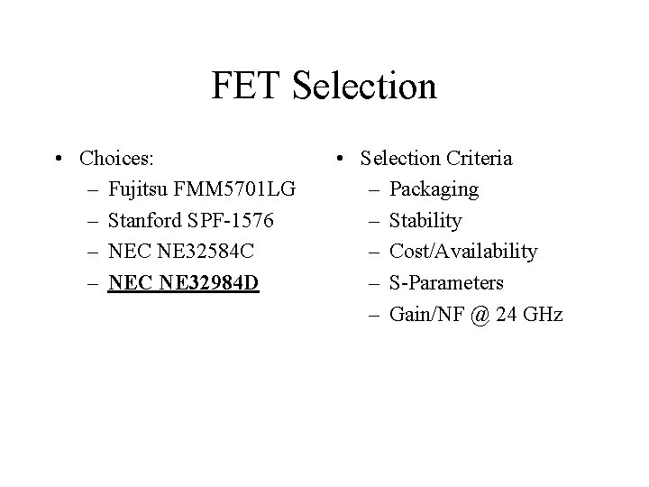
FET Selection • Choices: – Fujitsu FMM 5701 LG – Stanford SPF-1576 – NEC NE 32584 C – NEC NE 32984 D • Selection Criteria – Packaging – Stability – Cost/Availability – S-Parameters – Gain/NF @ 24 GHz

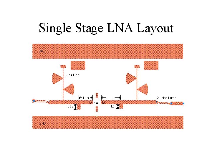
Single Stage LNA Layout

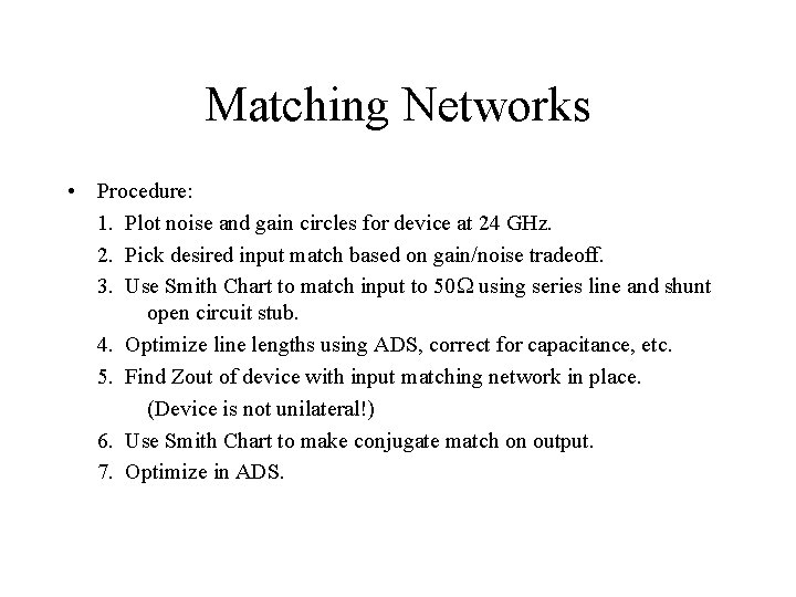
Matching Networks • Procedure: 1. Plot noise and gain circles for device at 24 GHz. 2. Pick desired input match based on gain/noise tradeoff. 3. Use Smith Chart to match input to 50 using series line and shunt open circuit stub. 4. Optimize line lengths using ADS, correct for capacitance, etc. 5. Find Zout of device with input matching network in place. (Device is not unilateral!) 6. Use Smith Chart to make conjugate match on output. 7. Optimize in ADS.

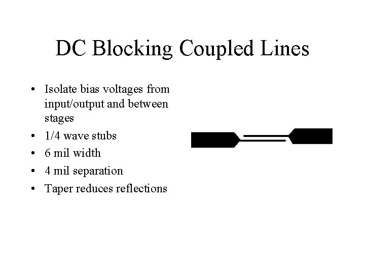
DC Blocking Coupled Lines • Isolate bias voltages from input/output and between stages • 1/4 wave stubs • 6 mil width • 4 mil separation • Taper reduces reflections

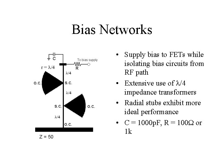
Bias Networks • Supply bias to FETs while isolating bias circuits from RF path • Extensive use of /4 impedance transformers • Radial stubs exhibit more ideal performance • C = 1000 p. F, R = 100 or 1 k

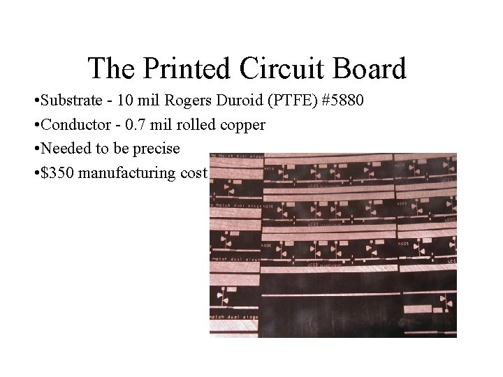
The Printed Circuit Board • Substrate - 10 mil Rogers Duroid (PTFE) #5880 • Conductor - 0. 7 mil rolled copper • Needed to be precise • $350 manufacturing cost

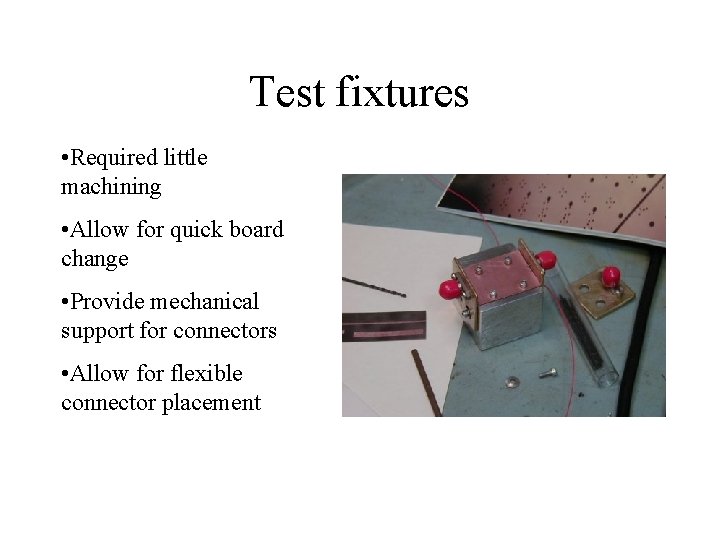
Test fixtures • Required little machining • Allow for quick board change • Provide mechanical support for connectors • Allow for flexible connector placement

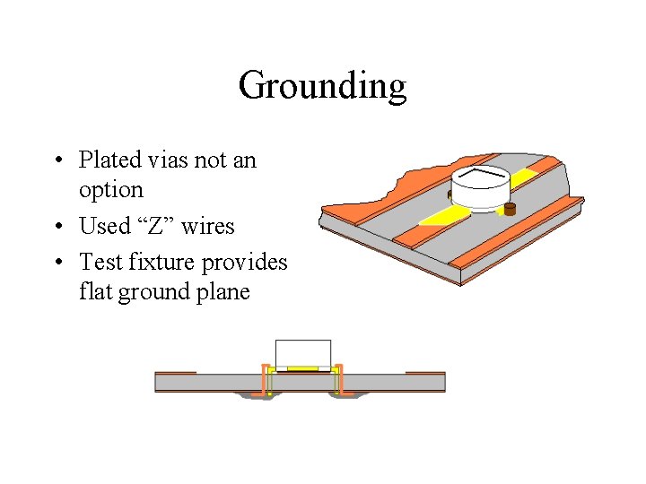
Grounding • Plated vias not an option • Used “Z” wires • Test fixture provides flat ground plane

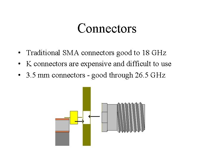
Connectors • Traditional SMA connectors good to 18 GHz • K connectors are expensive and difficult to use • 3. 5 mm connectors - good through 26. 5 GHz

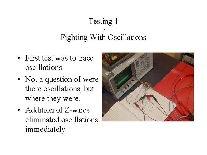
Testing 1 or Fighting With Oscillations • First test was to trace oscillations • Not a question of were there oscillations, but where they were. • Addition of Z-wires eliminated oscillations immediately

Testing 2 or Fighting With Calibration Standards • 3. 5 mm cal kit is VERY sensitive • Pin offsets of even fractions of a mm are detrimental

Noise Figure TBA. 0 d. B

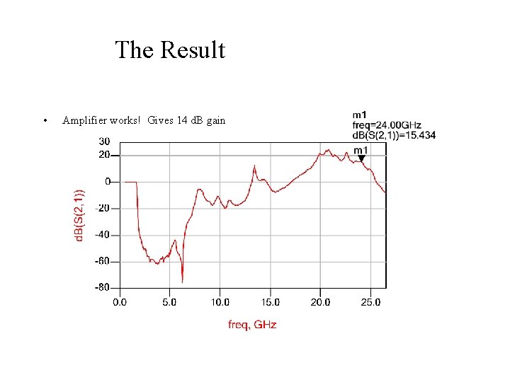
The Result • Amplifier works! Gives 14 d. B gain

What’s next? • Noise figure measurement • Waveguide transitions rather than coaxial connectors • Integration into receive downconverter • Re-tune for use as a low output power amplifier.