Ultrafast differential frontend electronics Detectors as signal generators

![To be decided: - with TOT ? And where ? On [E] or on To be decided: - with TOT ? And where ? On [E] or on](https://slidetodoc.com/presentation_image/2b13eabf24161445129e0f4e2bb706e2/image-27.jpg)
- Slides: 33

Ultra-fast differential front-end electronics • • Detectors as signal generators ~ Overview Low Z vs High Z Front-End Electronics (FEE), Differential vs. single ended FEE, Preliminary design & measurements G. Pascovici, IKP-Cologne, FEE Meeting, Saclay, 04 Dec. 2008

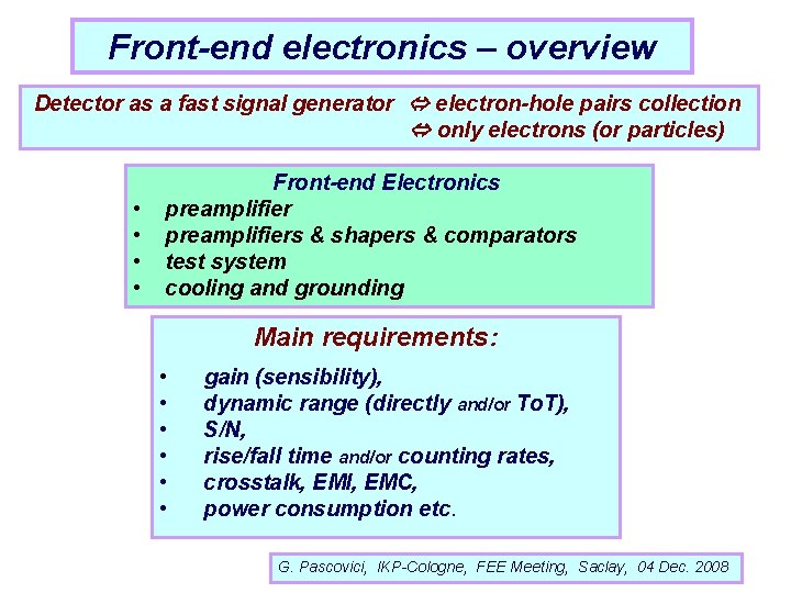
Front-end electronics – overview Detector as a fast signal generator electron-hole pairs collection only electrons (or particles) • • Front-end Electronics preamplifiers & shapers & comparators test system cooling and grounding Main requirements: • • • gain (sensibility), dynamic range (directly and/or To. T), S/N, rise/fall time and/or counting rates, crosstalk, EMI, EMC, power consumption etc. G. Pascovici, IKP-Cologne, FEE Meeting, Saclay, 04 Dec. 2008

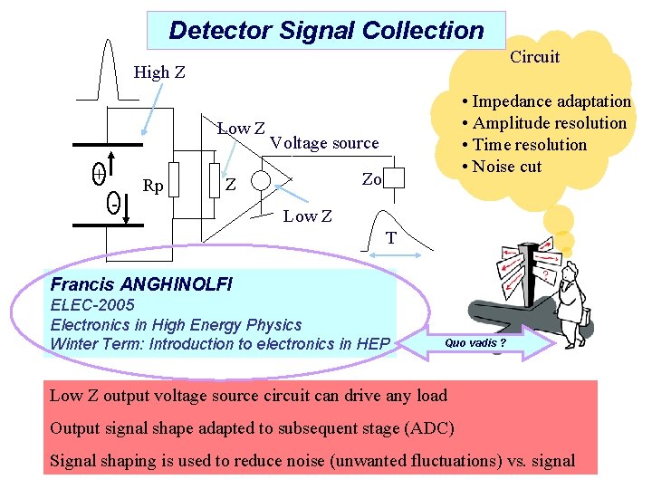
Detector Signal Collection Circuit High Z Low Z + - Rp • Impedance adaptation • Amplitude resolution • Time resolution • Noise cut Voltage source Zo Z Low Z T Francis ANGHINOLFI ELEC-2005 Electronics in High Energy Physics Winter Term: Introduction to electronics in HEP Quo vadis ? Low Z output voltage source circuit can drive any load Output signal shape adapted to subsequent stage (ADC) Signal shaping is used to reduce noise (unwanted fluctuations) vs. signal

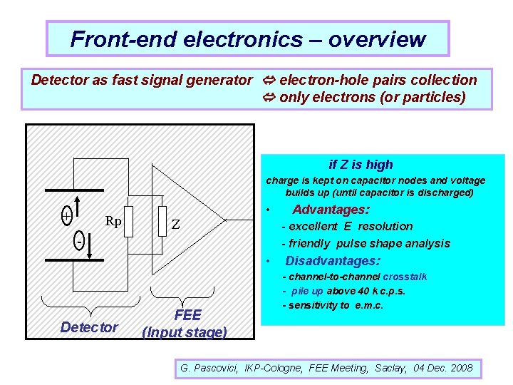
Front-end electronics – overview Detector as fast signal generator electron-hole pairs collection only electrons (or particles) if Z is high charge is kept on capacitor nodes and voltage builds up (until capacitor is discharged) + Rp Z • - excellent E resolution - friendly pulse shape analysis • Detector FEE (Input stage) Advantages: Disadvantages: - channel-to-channel crosstalk - pile up above 40 k c. p. s. - sensitivity to e. m. c. G. Pascovici, IKP-Cologne, FEE Meeting, Saclay, 04 Dec. 2008

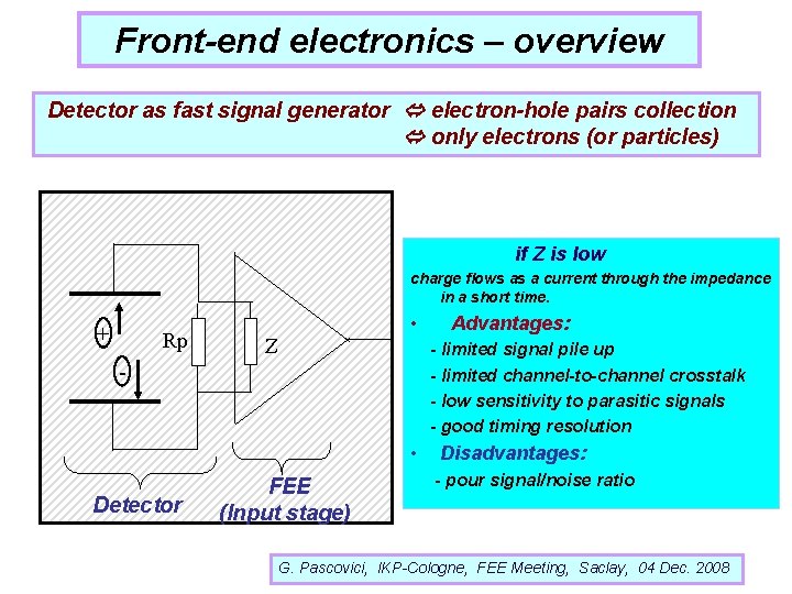
Front-end electronics – overview Detector as fast signal generator electron-hole pairs collection only electrons (or particles) if Z is low charge flows as a current through the impedance in a short time. + Rp Z • - limited signal pile up - limited channel-to-channel crosstalk - low sensitivity to parasitic signals - good timing resolution - • Detector FEE (Input stage) Advantages: Disadvantages: - pour signal/noise ratio G. Pascovici, IKP-Cologne, FEE Meeting, Saclay, 04 Dec. 2008

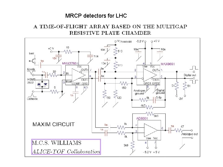
MRCP detectors for LHC

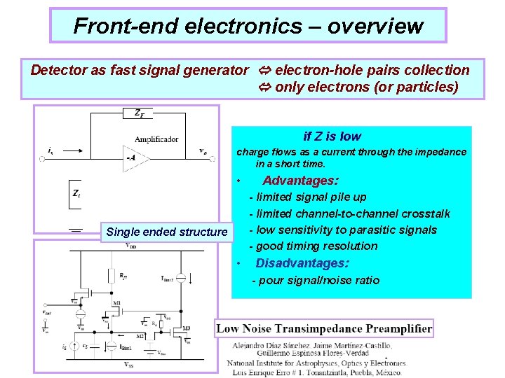
Front-end electronics – overview Detector as fast signal generator electron-hole pairs collection only electrons (or particles) if Z is low charge flows as a current through the impedance in a short time. • Advantages: - limited signal pile up - limited channel-to-channel crosstalk - low sensitivity to parasitic signals - good timing resolution Single ended structure • Disadvantages: - pour signal/noise ratio

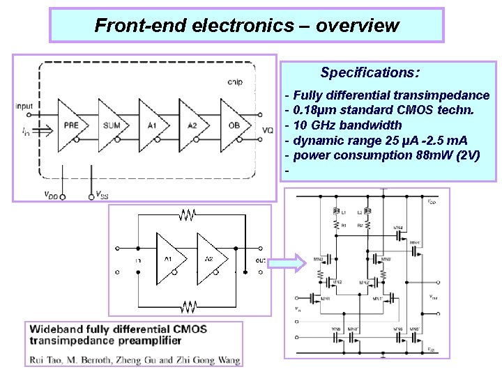
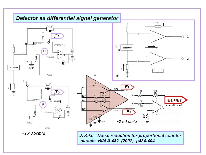
Front-end electronics – overview Specifications: - Fully differential transimpedance - 0. 18µm standard CMOS techn. - 10 GHz bandwidth - dynamic range 25 µA -2. 5 m. A - power consumption 88 m. W (2 V) -

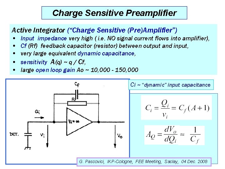
Charge Sensitive Preamplifier Active Integrator (“Charge Sensitive (Pre)Amplifier”) • • • Input impedance very high ( i. e. NO signal current flows into amplifier), Cf (Rf) feedback capacitor (resistor) between output and input, very large equivalent dynamic capacitance, sensitivity A(q) ~ q / Cf, large open loop gain Ao ~ 10, 000 - 150, 000 Ci ~ “dynamic” input capacitance Rf G. Pascovici, IKP-Cologne, FEE Meeting, Saclay, 04 Dec. 2008

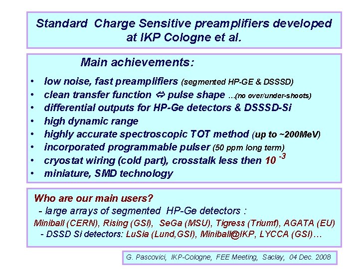
Standard Charge Sensitive preamplifiers developed at IKP Cologne et al. Main achievements: • • low noise, fast preamplifiers (segmented HP-GE & DSSSD) clean transfer function pulse shape …(no over/under-shoots) differential outputs for HP-Ge detectors & DSSSD-Si high dynamic range highly accurate spectroscopic TOT method (up to ~200 Me. V) incorporated programmable pulser (50 ppm long term) cryostat wiring (cold part), crosstalk less then 10 -3 miniature, SMD technology Who are our main users? - large arrays of segmented HP-Ge detectors : Miniball (CERN), Rising (GSI), Se. Ga (MSU), Tigress (Triumf), AGATA (EU) - DSSD Si detectors: Lu. Sia (Lund, GSI), Miniball@IKP, LYCCA (GSI)… G. Pascovici, IKP-Cologne, FEE Meeting, Saclay, 04 Dec. 2008

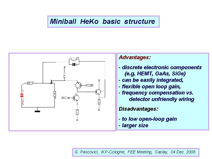
Miniball He. Ko basic structure Advantages: - discrete electronic components (e. g. HEMT, Ga. As, Si. Ge) - can be easily integrated, - flexible open loop gain, - frequency compensation vs. detector unfriendly wiring Disadvantages: - to low open-loop gain - larger size G. Pascovici, IKP-Cologne, FEE Meeting, Saclay, 04 Dec. 2008

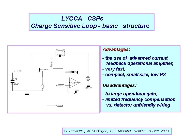
LYCCA CSPs Charge Sensitive Loop - basic structure Advantages: - the use of advanced current feedback operational amplifier, - very fast, - compact, small size, low PS Disadvantages: - to large open-loop gain, - limited frequency compensation vs. detector unfriendly wiring G. Pascovici, IKP-Cologne, FEE Meeting, Saclay, 04 Dec. 2008

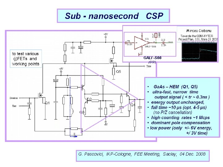
GALI -S 66 (GSI) G. Pascovici, IKP-Cologne, FEE Meeting, Saclay, 04 Dec. 2008

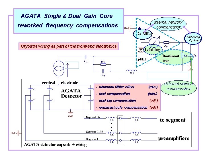
AGATA Single & Dual Gain Core reworked frequency compensations internal network compensation Lead comp. (1. Op. Amp) Cryostat wiring as part of the front-end electronics - minimum Miller effect (min. ) - lead compensation (min. ) - lead-lag compensation (adj. ) - dominant pole compensation (adj. ) external network compensation

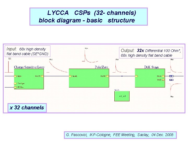
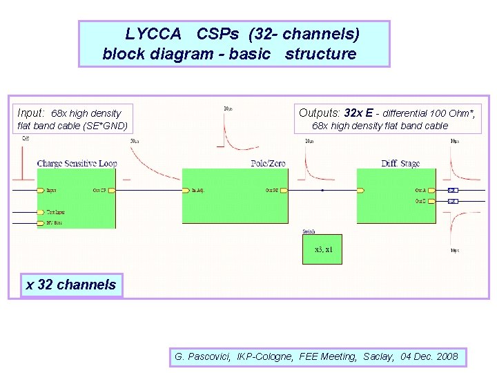
LYCCA CSPs (32 - channels) block diagram - basic structure Input: 68 x high density flat band cable (SE*GND) Output: 32 x Differential 100 Ohm*, 68 x high density flat band cable x 32 channels G. Pascovici, IKP-Cologne, FEE Meeting, Saclay, 04 Dec. 2008

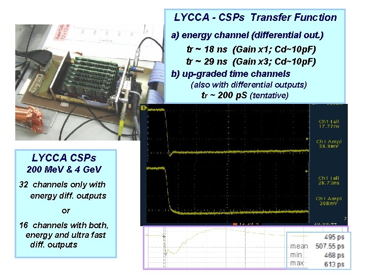
LYCCA - CSPs Transfer Function a) energy channel (differential out. ) tr ~ 18 ns (Gain x 1; Cd~10 p. F) tr ~ 29 ns (Gain x 3; Cd~10 p. F) b) up-graded time channels (also with differential outputs) tr ~ 200 p. S (tentative) LYCCA CSPs 200 Me. V & 4 Ge. V 32 channels only with energy diff. outputs or 16 channels with both, energy and ultra fast diff. outputs mean min max

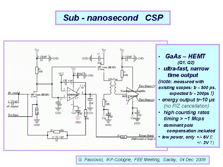
Sub - nanosecond CSP • Ga. As – HEMT (Q 1, Q 2) • ultra-fast, narrow time output (note: measured with existing scopes: tr ~ 500 ps, expected tr ~ 200 ps !) • energy output tf~10 µs (no P/Z cancellation) • high counting rates timing > ~1 Mcps • • dominant pole compensation included low power, only +/- 6 V E +/- 3 V T) G. Pascovici, IKP-Cologne, FEE Meeting, Saclay, 04 Dec. 2008

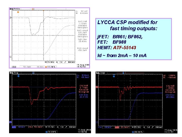
LYCCA CSP modified for fast timing outputs: j. FET: Bf 861; BF 862, FET: BF 988 HEMT: ATF-55143 Id ~ from 2 m. A – 10 m. A

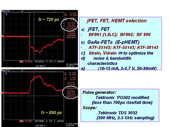
tr ~ 720 ps j. FET, HEMT selection a) j. FET, FET - BF 861 (1, B, C); BF 862; BF 889 b) Ga. As-FETs (E-p. HEMT) - ATF-35143; ATF-55143; ATF-38143 c) Idrain, Vdrain to optimize the d) noise & bandwidth characteristics e) (10 -15 m. A, 2 -2. 7 V, 20 -30 m. W) tr ~ 930 ps Pulse generator: Tektronix PG 502 modified (less than 700 ps rise/fall time) Scope: Tektronix TDS 3032 (300 MHz, 2. 5 GHz sampling)

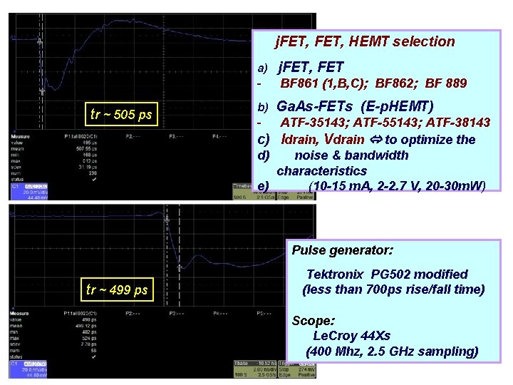
j. FET, HEMT selection tr ~ 505 ps a) j. FET, FET - BF 861 (1, B, C); BF 862; BF 889 b) Ga. As-FETs (E-p. HEMT) - ATF-35143; ATF-55143; ATF-38143 c) Idrain, Vdrain to optimize the d) noise & bandwidth characteristics e) (10 -15 m. A, 2 -2. 7 V, 20 -30 m. W) Pulse generator: tr ~ 499 ps Tektronix PG 502 modified (less than 700 ps rise/fall time) Scope: Le. Croy 44 Xs (400 Mhz, 2. 5 GHz sampling)

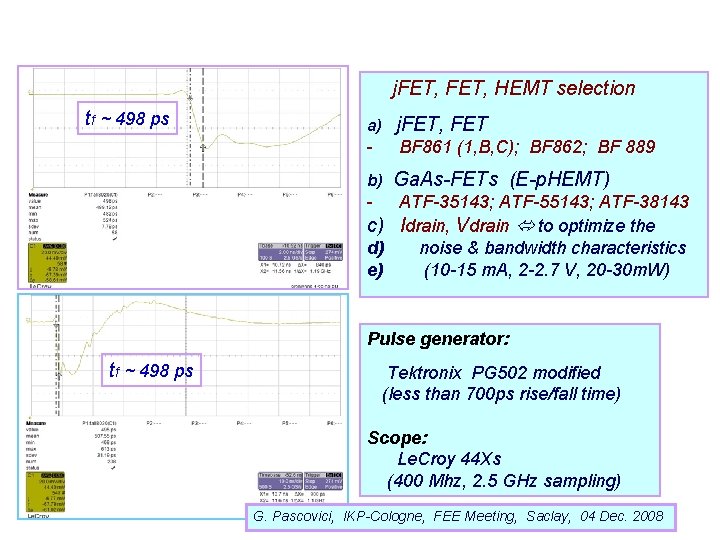
j. FET, HEMT selection tf ~ 498 ps a) j. FET, FET - BF 861 (1, B, C); BF 862; BF 889 b) Ga. As-FETs (E-p. HEMT) - ATF-35143; ATF-55143; ATF-38143 c) Idrain, Vdrain to optimize the d) noise & bandwidth characteristics e) (10 -15 m. A, 2 -2. 7 V, 20 -30 m. W) Pulse generator: tf ~ 498 ps Tektronix PG 502 modified (less than 700 ps rise/fall time) Scope: Le. Croy 44 Xs (400 Mhz, 2. 5 GHz sampling) G. Pascovici, IKP-Cologne, FEE Meeting, Saclay, 04 Dec. 2008

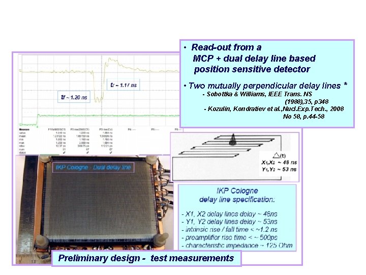
• Read-out from a MCP + dual delay line based position sensitive detector • Two mutually perpendicular delay lines * - Sobottka & Williams, IEEE Trans. NS (1988), 35, p 348 - Kozulin, Kondratiev et al. , Nucl. Exp. Tech. , 2008 No 58, p. 44 -58 Preliminary design - test measurements

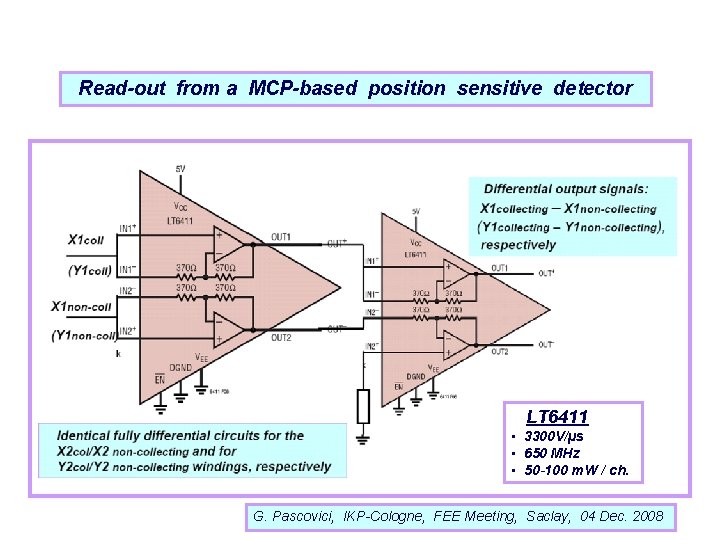
Read-out from a MCP-based position sensitive detector LT 6411 • 3300 V/µs • 650 MHz • 50 -100 m. W / ch. G. Pascovici, IKP-Cologne, FEE Meeting, Saclay, 04 Dec. 2008

LYCCA CSPs (32 - channels) block diagram - basic structure Input: 68 x high density flat band cable (SE*GND) Outputs: 32 x E - differential 100 Ohm*, 68 x high density flat band cable x 32 channels G. Pascovici, IKP-Cologne, FEE Meeting, Saclay, 04 Dec. 2008

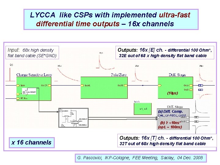
LYCCA like CSPs with implemented ultra-fast differential time outputs – 16 x channels Input: 68 x high density Outputs: 16 x [E] ch. - differential 100 Ohm*, flat band cable (SE*GND) 32 E out of 68 x high density flat band cable (10µs) (a) Diff. Comp. CML, LV-PECL, LVDS (b) tf ~10 ns* (opt. ~ 100 ns) x 16 channels Outputs: 16 x [T] ch. - differential 100 Ohm*, 32 T out of 68 x high density flat band cable G. Pascovici, IKP-Cologne, FEE Meeting, Saclay, 04 Dec. 2008

To be decided: - with TOT ? - with spectroscopic TOT ? - differential signals standard: PECL, NECL, CML ?
![To be decided with TOT And where On E or on To be decided: - with TOT ? And where ? On [E] or on](https://slidetodoc.com/presentation_image/2b13eabf24161445129e0f4e2bb706e2/image-27.jpg)
To be decided: - with TOT ? And where ? On [E] or on [T] channel ? - with spectroscopic TOT ? Or quasi spectroscopic? - differential signals standard: PECL, NECL, CML ? TOT circuitry? - requirements has to be decided ? -E or/and T ch. ?

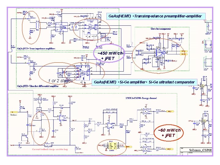
Ga. As(HEMT) +Transimpedance preamplifier-amplifier ~450 m. W/ch + j. FET 1 or 2 stages Ga. As(HEMT) +Si-Ge amplifier+ Si-Ge ultrafast comparator ~60 m. W/ch + j. FET

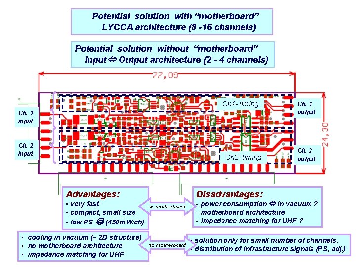
Potential solution with “motherboard” LYCCA architecture (8 -16 channels) Potential solution without “motherboard” Input Output architecture (2 - 4 channels) Ch 1 - timing Ch. 1 input Ch. 2 input Ch 2 - timing Advantages: • very fast • compact, small size • low PS (450 m. W/ch) • cooling in vacuum (~ 2 D structure) • no motherboard architecture • impedance matching for UHF Ch. 1 output Ch. 2 output Disadvantages: w. motherboard no motherboard - power consumption in vacuum ? - motherboard architecture - impedance matching for UHF ? • solution only for small number of channels, • distribution of infrastructure signals (PS, adj. )

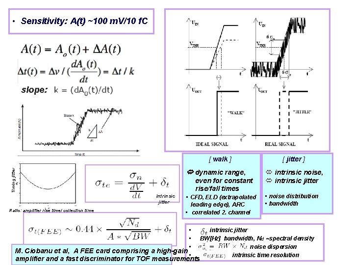
• Sensitivity: A(t) ~100 m. V/10 f. C slope: Timing jitter [ walk ] dynamic range, even for constant rise/fall times Intrinsic jitter Ratio: amplifier rise time/ collection time • CFD, ELD (extrapolated leading edge), ARC • correlated 2. channel [ jitter ] ó intrinsic noise, ó intrinsic jitter • noise distribution • bandwidth • intrinsic jitter • BW[Hz] bandwidth, Nd ~spectral density • noise dispersion M. Ciobanu et al, A FEE card comprising a high-gain • intrinsic time resolution amplifier and a fast discriminator for TOF measurements

IE 1 I+IE 2 I


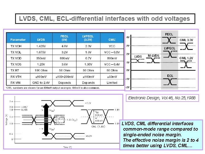
Electronic Design, Vol. 46, No. 25, 1988 LVDS, CML differential interfaces common-mode range compared to single-ended noise margin. The effective noise margin is 2 to 4 times better using LVDS, CML…