Towards passive terahertz imaging using a semiconductor quantum

- Slides: 27

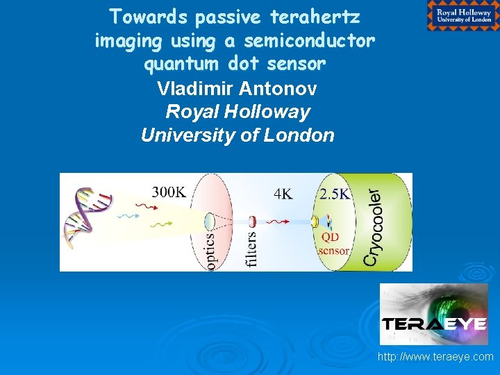
Towards passive terahertz imaging using a semiconductor quantum dot sensor Vladimir Antonov Royal Holloway University of London http: //www. teraeye. com

Acknowledgments Royal Holloway, UK : H Hashiba Tokyo University&JST, Japan: Prof. S Komiyama, Drs. J Chen, O Astafiev (NEC) ISSP RAN, Russia: Dr. L Kulik NPL, UK: Dr A Tzalenchuk, Dr S Gibling and P Kleinschmidt Chalmers University, Sweden: Prof. P Delsing, Dr S Kubatkin Optisense LTD: M Andreo

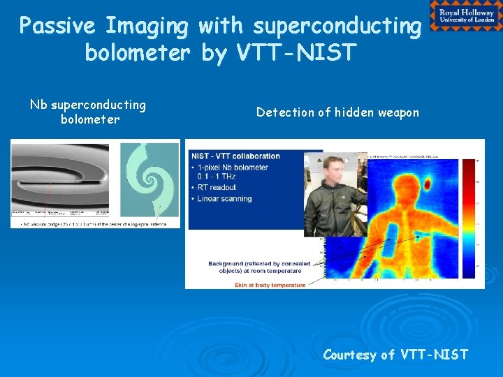
Passive Imaging with superconducting bolometer by VTT-NIST Nb superconducting bolometer Detection of hidden weapon Courtesy of VTT-NIST

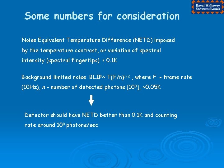
Some numbers for consideration Noise Equivalent Temperature Difference (NETD) imposed by the temperature contrast, or variation of spectral intensity (spectral fingertips) < 0. 1 K Background limited noise BLIP~ T(F/n)1/2 , where F - frame rate (10 Hz), n - number of detected photons (108), ~0. 05 K Detector should have NETD better than 0. 1 K and counting rate around 108 photons/sec

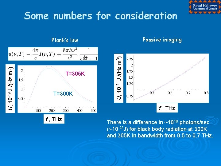
Some numbers for consideration Passive imaging T=305 K T=300 K U, 10 -21 J /(Hz m 3) U, 10 -19 J /(Hz m 3) Plank’s law f , THz There is a difference in ~1010 photons/sec (~10 -23 J) for black body radiation at 300 K and 305 K in bandwidth from 0. 5 to 0. 7 THz.

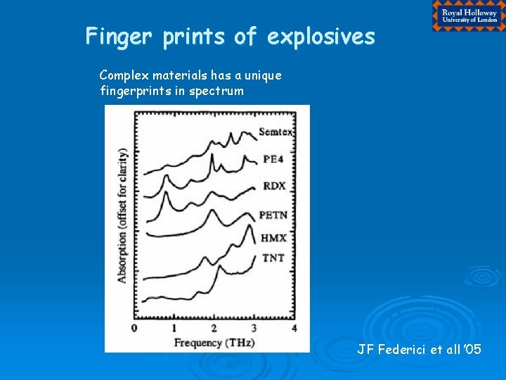
Finger prints of explosives Complex materials has a unique fingerprints in spectrum T=300 K JF Federici et all ’ 05

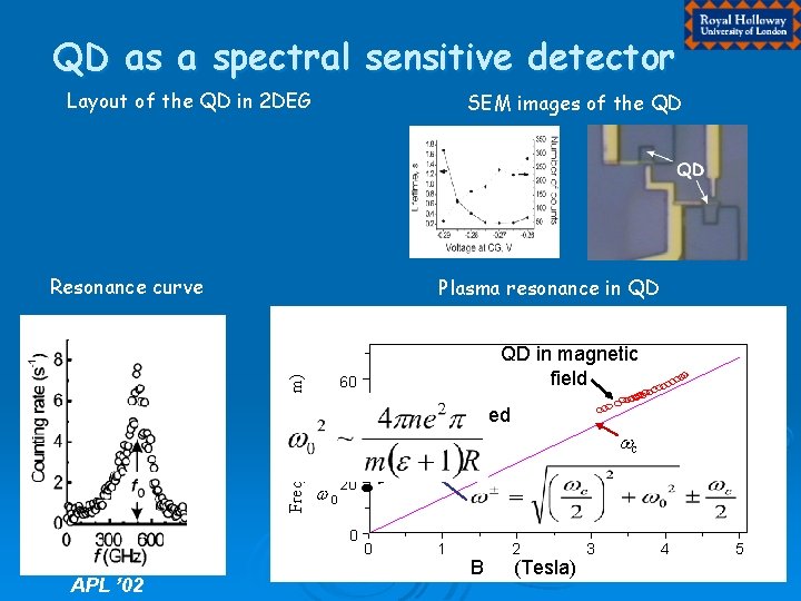
QD as a spectral sensitive detector Layout of the QD in 2 DEG SEM images of the QD Resonance curve Frequency (/cm) Plasma resonance in QD 60 Zero filed 40 0 c 20 0 APL ’ 02 QD in magnetic field 0 1 B 2 (Tesla) 3 4 5

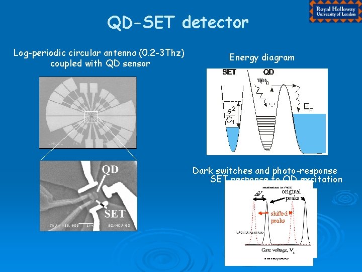
QD-SET detector Log-periodic circular antenna (0. 2 -3 Thz) coupled with QD sensor Energy diagram Dark switches and photo-response SET response to QD excitation DVg original peaks shifted peaks

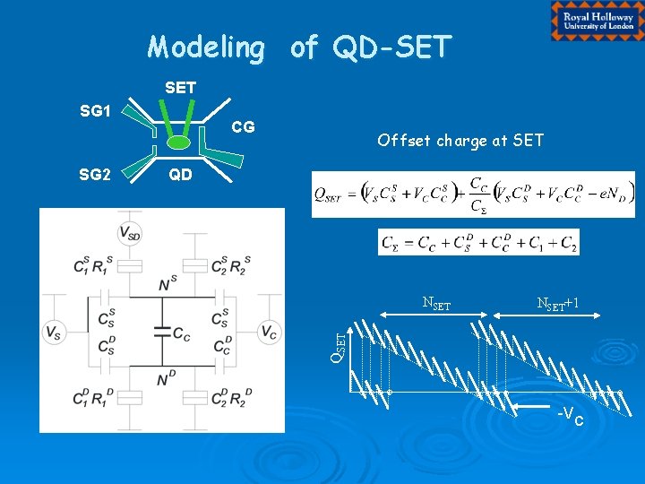
Modeling of QD-SET SG 1 Offset charge at SET QD NSET+1 QSET SG 2 CG -Vc

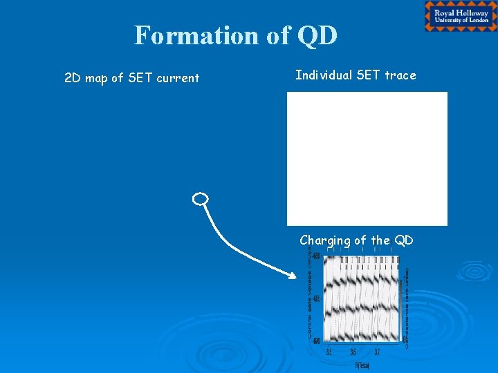
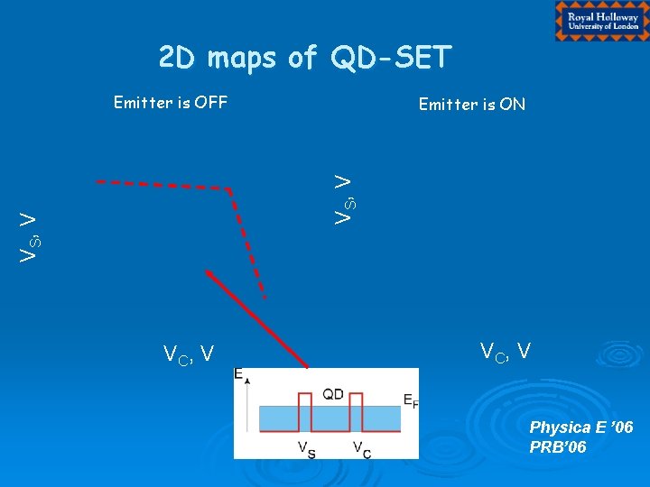
Formation of QD 2 D map of SET current Individual SET trace Charging of the QD

Photosignal at 0. 3 K T=0. 05 K T=0. 3 K

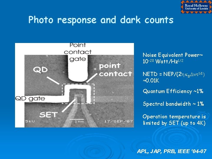
Photo response and dark counts Noise Equivalent Power~ 10 -20 Watt/Hz 1/2 NETD = NEP/(2 hk. BDnt 1/2) ~0. 01 K Quantum Efficiency ~1% Spectral bandwidth ~ 1% Operation temperature is limited by SET (up to 4 K) APL, JAP, PRB, IEEE ’ 04 -07

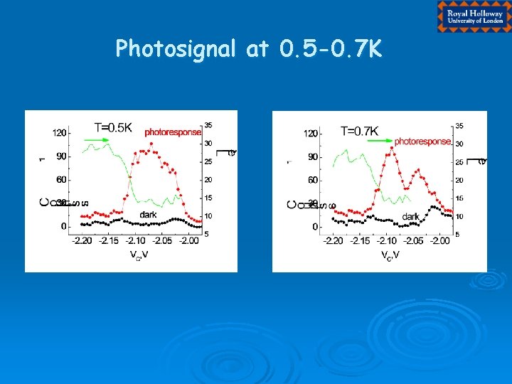
Photosignal at 0. 5 -0. 7 K

2 D maps of QD-SET Emitter is OFF V S, V Emitter is ON V C, V Physica E ’ 06 PRB’ 06

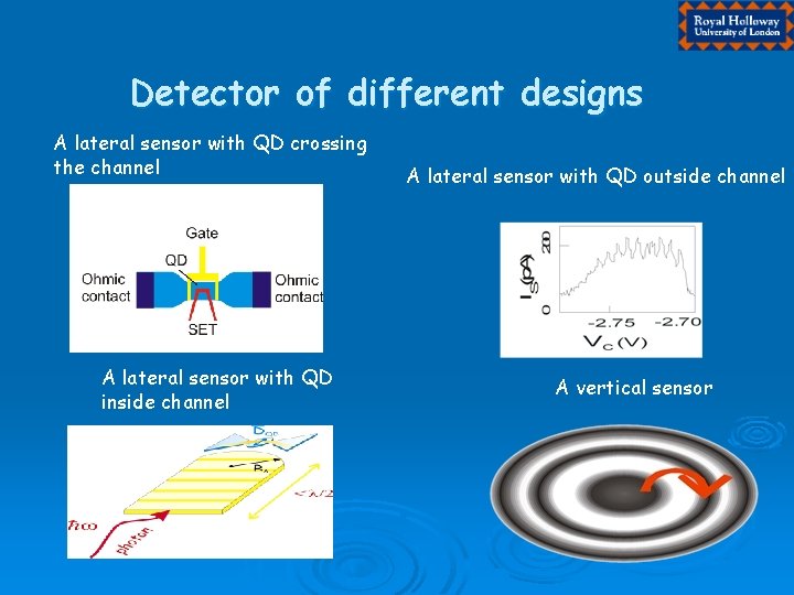
Detector of different designs A lateral sensor with QD crossing the channel A lateral sensor with QD inside channel A lateral sensor with QD outside channel A vertical sensor

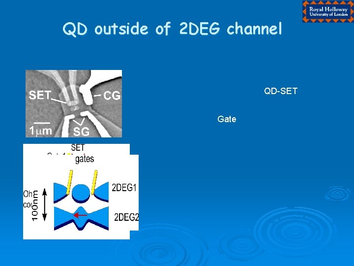
QD outside of 2 DEG channel QD-SET Gate

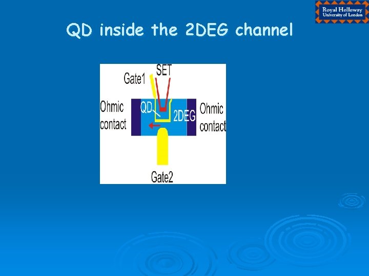
QD inside the 2 DEG channel

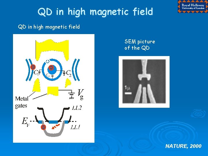
QD in high magnetic field SEM picture of the QD 1 m LL 1 LL 0 NATURE, 2000

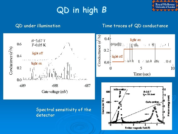
QD in high B QD under illumination Spectral sensitivity of the detector Time traces of QD conductance

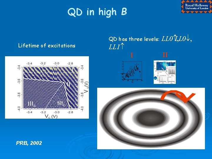
QD in high B Lifetime of excitations QD has three levels: LL 1 I PRB, 2002 LL 0 , LL 0¯, II

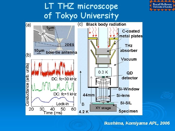
LT THZ microscope of Tokyo University Ikushima, Komiyama APL, 2006

LT THZ microscope of Tokyo University

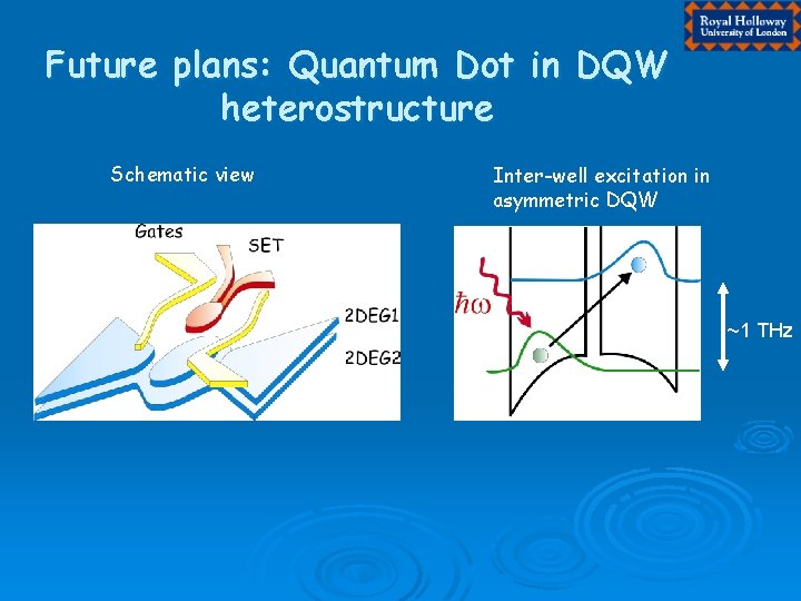
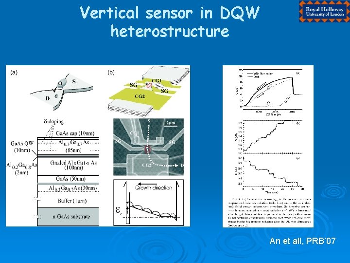
Future plans: Quantum Dot in DQW heterostructure Schematic view Inter-well excitation in asymmetric DQW ~1 THz

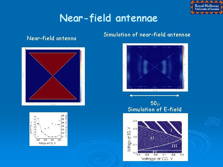
Near-field antennae Near-field antenna Simulation of near-field antennae 50 m Simulation of E-field

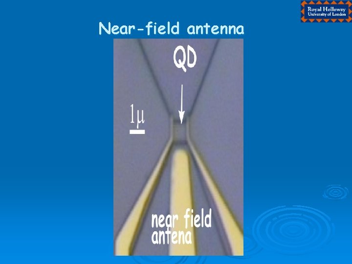
Near-field antenna

Challenges QD detector: which type? Room Temperature Imaging Source of THz radiation for in-situ calibration • Physics of isolated QD in DW heterostructures

Vertical sensor in DQW heterostructure An et all, PRB’ 07