SYEN 3330 Digital Systems Chapter 9 Part 1
- Slides: 23

SYEN 3330 Digital Systems Chapter 9 – Part 1 SYEN 3330 Digital Systems Jung H. Kim 1

Overview of Chapter 9 • Memory Definitions • Random Access Memory § Function § Operation § Timing • RAM Integrated Circuits § § § RAM Cell RAM Bit Slice 3 -State Buffers Cell Arrays and Coincident Selection Dynamic RAM • Array of RAM Integrated Circuits • Arrays of Static and Dynamic RAMs SYEN 3330 Digital Systems 2

Memory Definitions SYEN 3330 Digital Systems 3

Memory Definitions (Continued) SYEN 3330 Digital Systems 4

Memory Organization SYEN 3330 Digital Systems 5

Memory Block Diagram SYEN 3330 Digital Systems 6

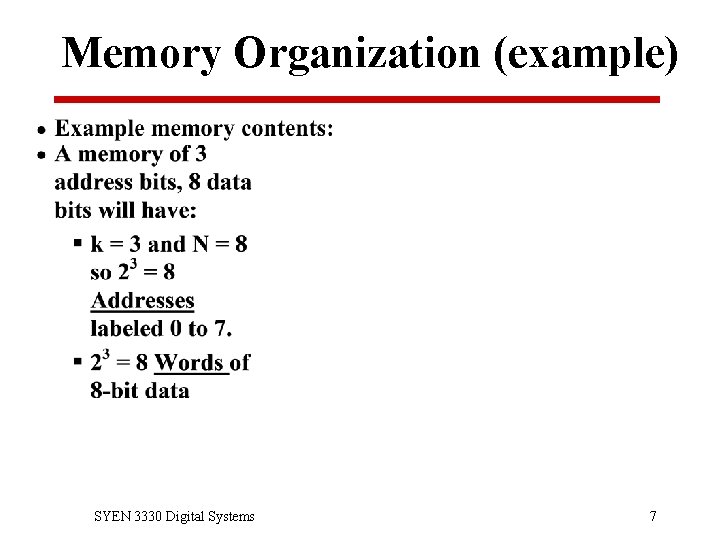
Memory Organization (example) SYEN 3330 Digital Systems 7

Basic Memory Operations SYEN 3330 Digital Systems 8

Basic Memory Operations (Continued) SYEN 3330 Digital Systems 9

Memory Operation Timing • The most basic memories are asynchronous § Storage is performed by latches or storage of electrical charge § Do not use a clock • Controlled by application of control inputs and address • Timing of signal application is critical to the operation SYEN 3330 Digital Systems 10

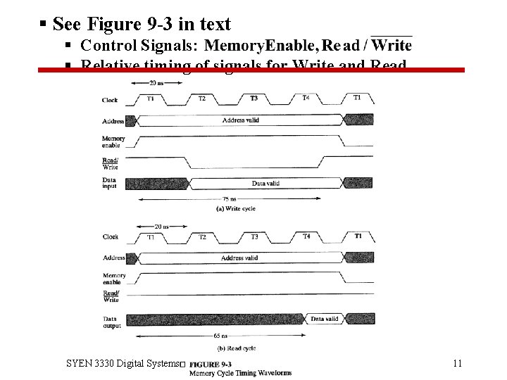
§ See Figure 9 -3 in text § Control Signals: § Relative timing of signals for Write and Read SYEN 3330 Digital Systems 11

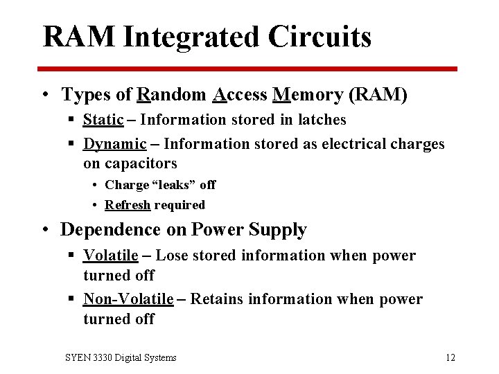
RAM Integrated Circuits • Types of Random Access Memory (RAM) § Static – Information stored in latches § Dynamic – Information stored as electrical charges on capacitors • Charge “leaks” off • Refresh required • Dependence on Power Supply § Volatile – Lose stored information when power turned off § Non-Volatile – Retains information when power turned off SYEN 3330 Digital Systems 12

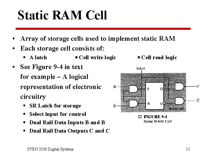
Static RAM Cell • Array of storage cells used to implement static RAM • Each storage cell consists of: § A latch Cell write logic Cell read logic • See Figure 9 -4 in text for example – A logical representation of electronic circuitry § § SR Latch for storage Select input for control Dual Rail Data Inputs B and B Dual Rail Data Outputs C and C SYEN 3330 Digital Systems 13

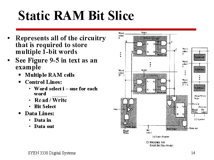
Static RAM Bit Slice • Represents all of the circuitry that is required to store multiple 1 -bit words • See Figure 9 -5 in text as an example § Multiple RAM cells § Control Lines: • Word select i – one for each word • • Bit Select § Data Lines: • Data in • Data out SYEN 3330 Digital Systems 14

n-Word 1 -Bit RAM IC • To build a RAM IC from a RAM slice, we need: – A decoder to decode the log 2 n address lines to n word select lines – A 3 -state buffer on the data output to permit RAM ICs to be combined into a RAM with c n words SYEN 3330 Digital Systems 15

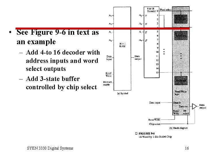
• See Figure 9 -6 in text as an example – Add 4 -to 16 decoder with address inputs and word select outputs – Add 3 -state buffer controlled by chip select SYEN 3330 Digital Systems 16

3 -state Buffers and Logic SYEN 3330 Digital Systems 17

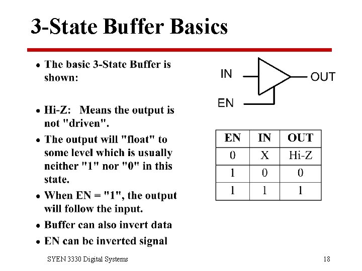
3 -State Buffer Basics SYEN 3330 Digital Systems 18

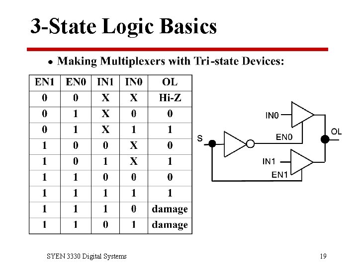
3 -State Logic Basics SYEN 3330 Digital Systems 19

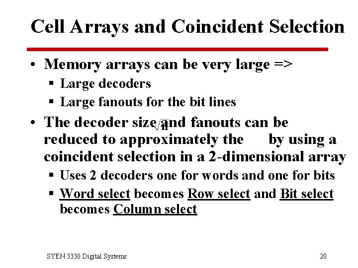
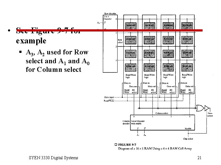
Cell Arrays and Coincident Selection • Memory arrays can be very large => § Large decoders § Large fanouts for the bit lines • The decoder size and fanouts can be reduced to approximately the by using a coincident selection in a 2 -dimensional array § Uses 2 decoders one for words and one for bits § Word select becomes Row select and Bit select becomes Column select SYEN 3330 Digital Systems 20

• See Figure 9 -7 for example § A 3, A 2 used for Row select and A 1 and A 0 for Column select SYEN 3330 Digital Systems 21

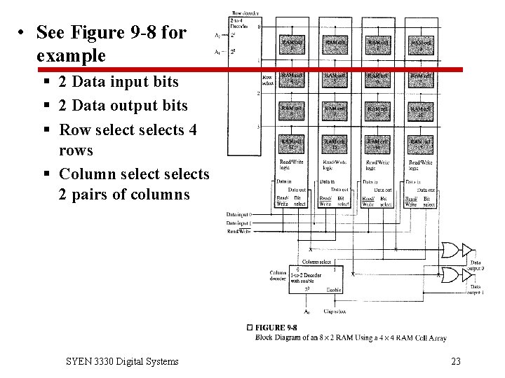
RAM ICs with > 1 Bit/Word • Word length can be quite high. • To better balance the number of words and word length, use ICs with > 1 bit/word SYEN 3330 Digital Systems 22

• See Figure 9 -8 for example § 2 Data input bits § 2 Data output bits § Row selects 4 rows § Column selects 2 pairs of columns SYEN 3330 Digital Systems 23