SYEN 3330 Digital Systems Chapter 6 Part 4
- Slides: 23

SYEN 3330 Digital Systems Chapter 6 – Part 4 SYEN 3330 Digital Systems Jung H. Kim 1

Overview of Chapter 6 • Types of Sequential Circuits • Storage Elements – Latches – Flip-Flops • Sequential Circuit Analysis – State Tables – State Diagrams • Sequential Circuit Design – – Specification Assignment of State Codes Implementation HDL Representation SYEN 3330 Digital Systems 2

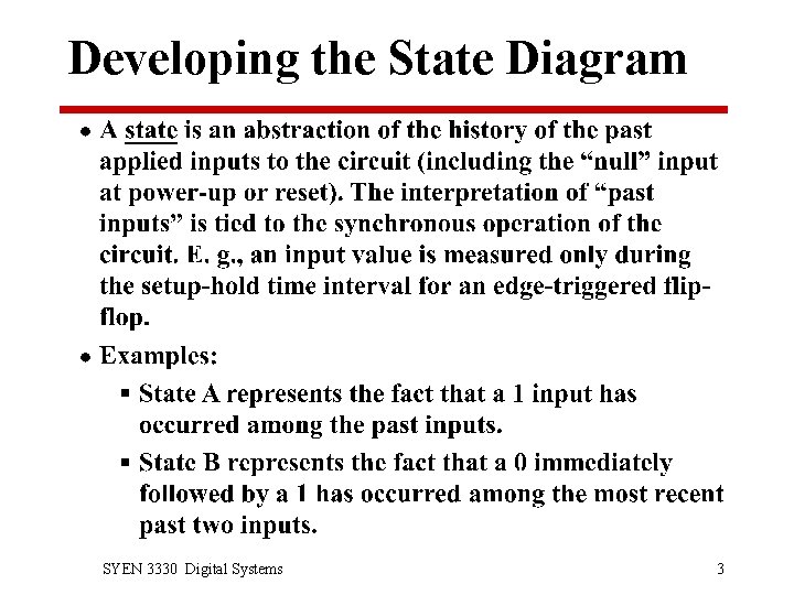
Developing the State Diagram SYEN 3330 Digital Systems 3

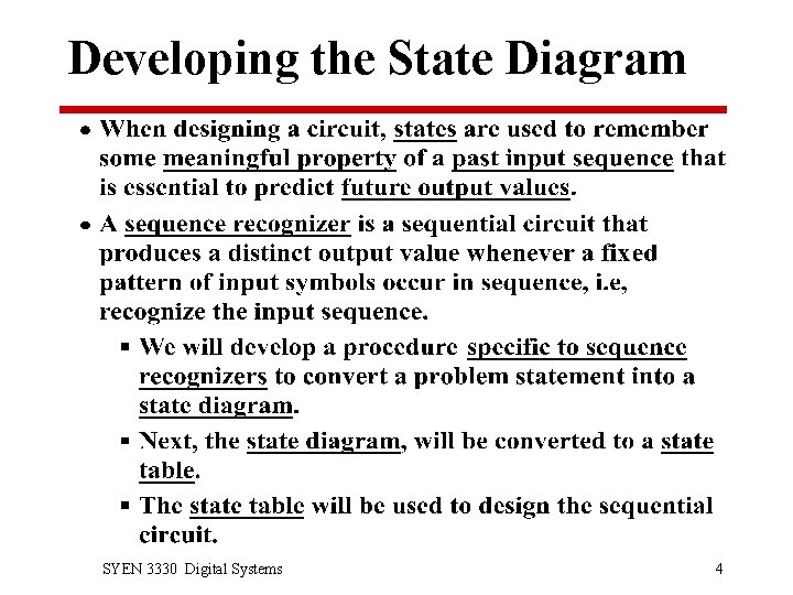
Developing the State Diagram SYEN 3330 Digital Systems 4

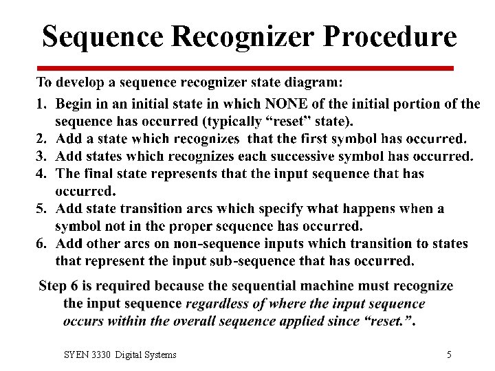
Sequence Recognizer Procedure SYEN 3330 Digital Systems 5

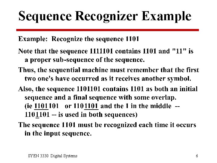
Sequence Recognizer Example SYEN 3330 Digital Systems 6

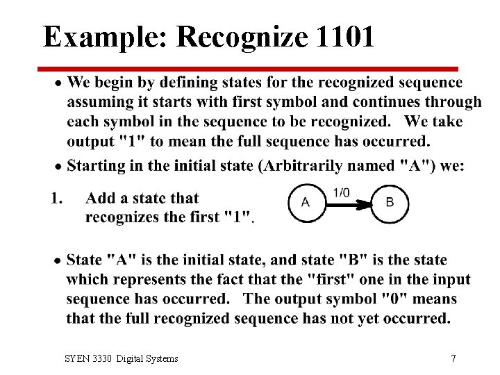
Example: Recognize 1101 SYEN 3330 Digital Systems 7

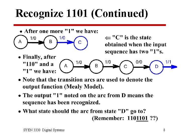
Recognize 1101 (Continued) SYEN 3330 Digital Systems 8

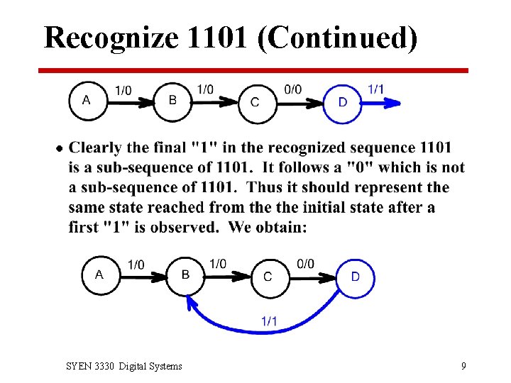
Recognize 1101 (Continued) SYEN 3330 Digital Systems 9

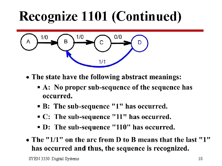
Recognize 1101 (Continued) SYEN 3330 Digital Systems 10

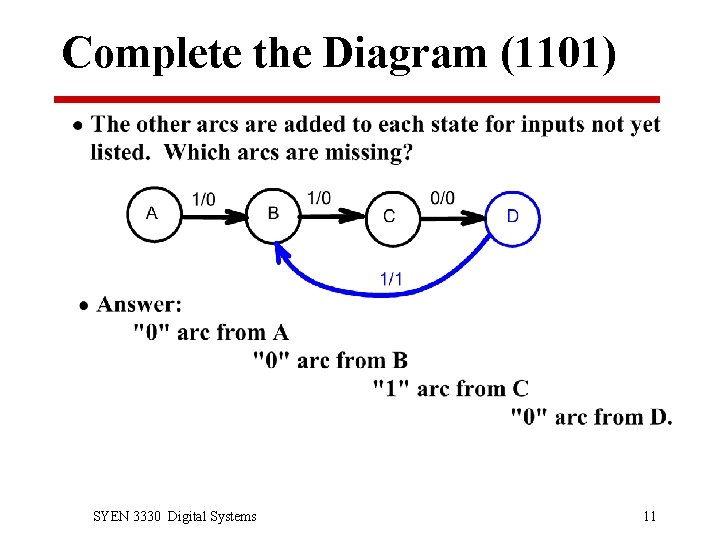
Complete the Diagram (1101) SYEN 3330 Digital Systems 11

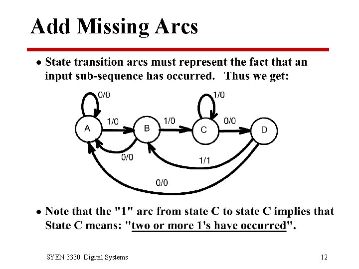
Add Missing Arcs SYEN 3330 Digital Systems 12

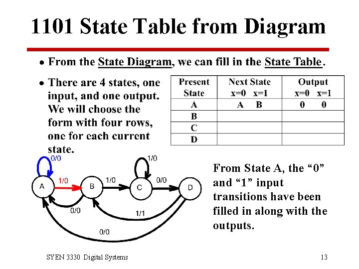
1101 State Table from Diagram From State A, the “ 0” and “ 1” input transitions have been filled in along with the outputs. SYEN 3330 Digital Systems 13

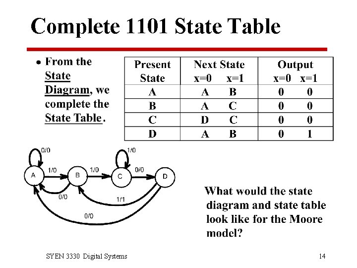
Complete 1101 State Table SYEN 3330 Digital Systems 14

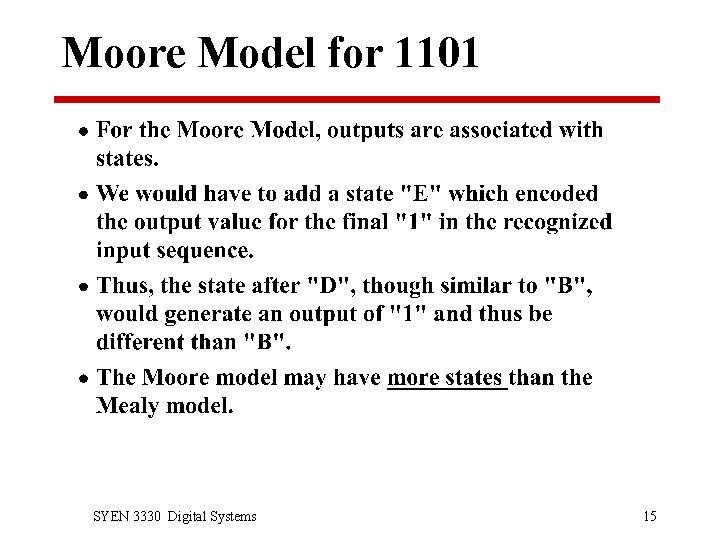
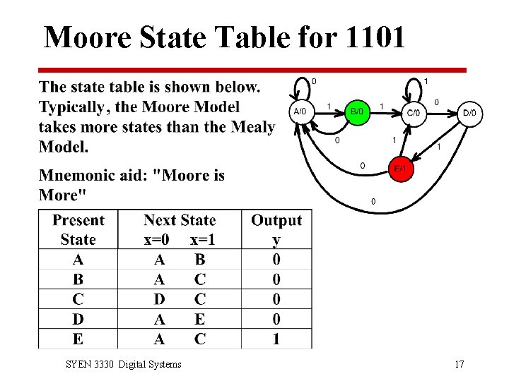
Moore Model for 1101 SYEN 3330 Digital Systems 15

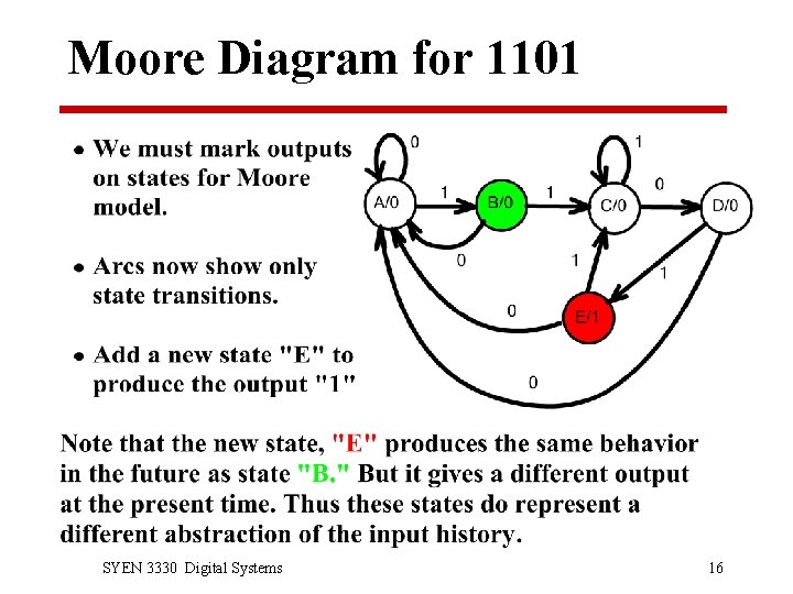
Moore Diagram for 1101 SYEN 3330 Digital Systems 16

Moore State Table for 1101 SYEN 3330 Digital Systems 17

Second State Diagram Example • A register consists of an ordered set of n flip-flops plus combinational logic to determine its next state. • If a register can be designed as a set of n identical cells, the register cell can be designed as a two-state sequential circuit. • Next we will consider such as example. SYEN 3330 Digital Systems 18

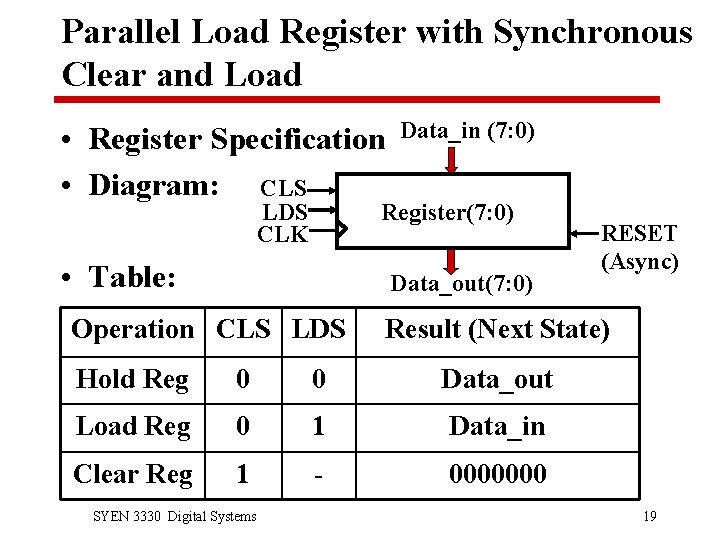
Parallel Load Register with Synchronous Clear and Load • Register Specification • Diagram: CLS Data_in (7: 0) Register(7: 0) LDS CLK • Table: Data_out(7: 0) Operation CLS LDS Result (Next State) Hold Reg 0 0 Data_out Load Reg 0 1 Data_in Clear Reg 1 - 0000000 SYEN 3330 Digital Systems RESET (Async) 19

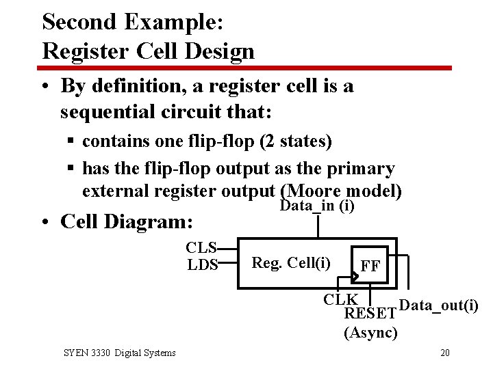
Second Example: Register Cell Design • By definition, a register cell is a sequential circuit that: § contains one flip-flop (2 states) § has the flip-flop output as the primary external register output (Moore model) • Cell Diagram: CLS LDS Data_in (i) Reg. Cell(i) FF CLK RESET Data_out(i) (Async) SYEN 3330 Digital Systems 20

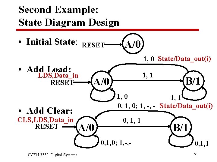
Second Example: State Diagram Design • Initial State: RESET A/0 1, 0 State/Data_out(i) • Add Load: LDS, Data_in RESET A/0 0, 1, 1 0, 1, 0; 1, -, - SYEN 3330 Digital Systems B/1 1, 0 1, 1 0, 1, 0; 1, -, - State/Data_out(i) • Add Clear: CLS, LDS, Data_in RESET 1, 1 B/1 0, 1, 1 21

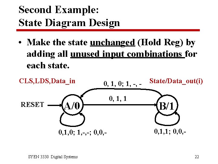
Second Example: State Diagram Design • Make the state unchanged (Hold Reg) by adding all unused input combinations for each state. CLS, LDS, Data_in RESET 0, 1, 0; 1, -, - A/0 0, 1, 0; 1, -, -; 0, 0, - SYEN 3330 Digital Systems 0, 1, 1 State/Data_out(i) B/1 0, 1, 1; 0, 0, - 22

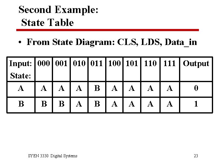
Second Example: State Table • From State Diagram: CLS, LDS, Data_in Input: 000 001 010 011 100 101 110 111 Output State: A A B A A 0 B B B A SYEN 3330 Digital Systems B A A 1 23