Semiconductor Devices 25 Atsufumi Hirohata Department of Electronics
- Slides: 15

Semiconductor Devices 25 Atsufumi Hirohata Department of Electronics 11: 00 Monday, 1/December/2014 (P/L 005)

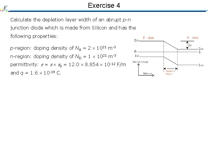
Exercise 4 Calculate the depletion layer width of an abrupt p-n junction diode which is made from Silicon and has the following properties: p-region: doping density of NA = 2 1021 m-3 n-region: doping density of ND = 1 1021 m-3 permittivity: e = e e 0 = 12. 0 8. 854 10 -12 F/m and q = 1. 6 10 -19 C.

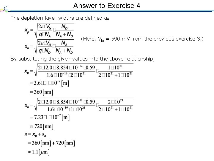
Answer to Exercise 4 The depletion layer widths are defined as (Here, Vbi = 590 m. V from the previous exercise 3. ) By substituting the given values into the above relationship,

25 Metal Semiconductor Junction • Work function • Metal / n-type semiconductor • Metal / p-type semiconductor Einstein relationship • • Schottky barrier

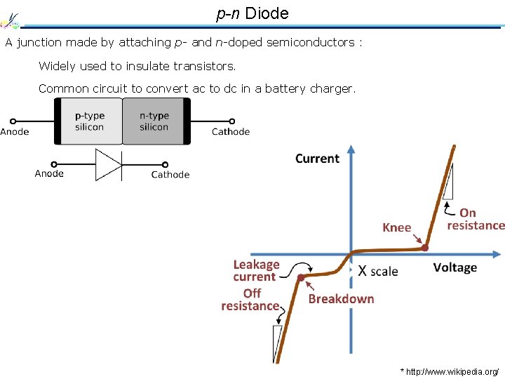
p-n Diode A junction made by attaching p- and n-doped semiconductors : Widely used to insulate transistors. Common circuit to convert ac to dc in a battery charger. * http: //www. wikipedia. org/

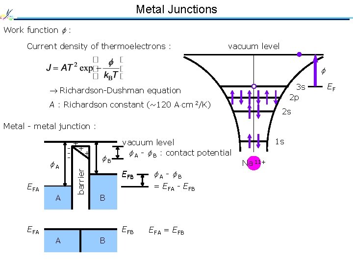
Metal Junctions Work function : Current density of thermoelectrons : vacuum level 3 s 2 p Richardson-Dushman equation A : Richardson constant (~120 A cm 2/K) 2 s Metal - metal junction : EFA A EFA barrier A + - + + - B vacuum level A - B : contact potential EFB = EFA - EFB B EFB A A - B B EFA = EFB 1 s Na 11+ EF

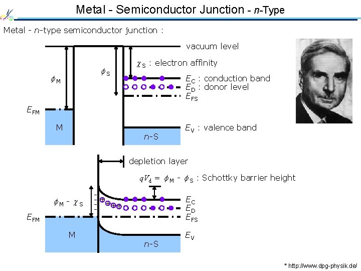
Metal - Semiconductor Junction - n-Type Metal - n-type semiconductor junction : vacuum level S M S : electron affinity EC : conduction band ED : donor level EFS EFM M n-S EV : valence band depletion layer q. Vd = M - S : Schottky barrier height M - S EFM M - ++ ++ - EC ED EFS n-S EV * http: //www. dpg-physik. de/

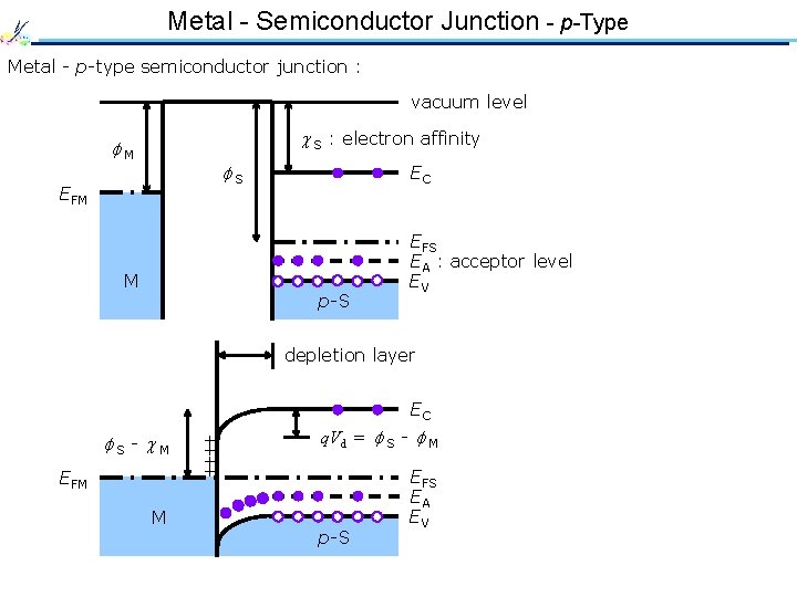
Metal - Semiconductor Junction - p-Type Metal - p-type semiconductor junction : vacuum level S : electron affinity M S EFM M EC p-S EFS EA : acceptor level EV depletion layer EC S - M EFM M + + q. Vd = S - M p-S EFS EA EV

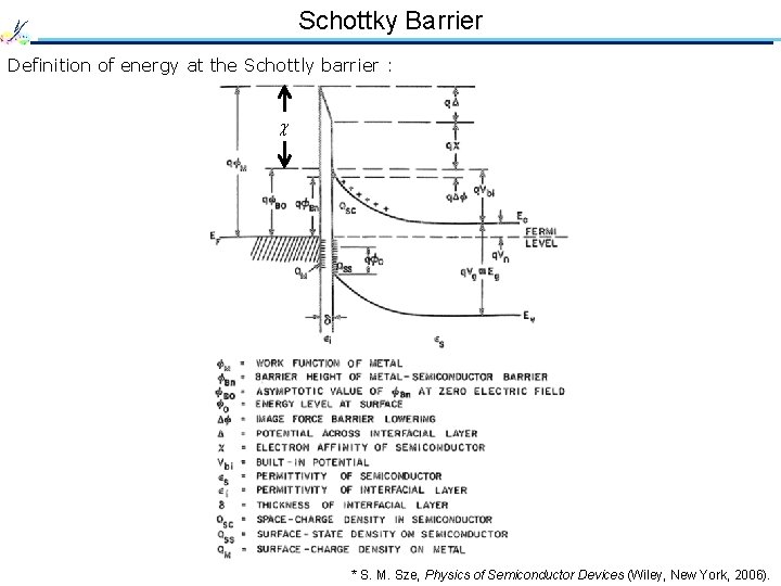
Schottky Barrier Definition of energy at the Schottly barrier : * S. M. Sze, Physics of Semiconductor Devices (Wiley, New York, 2006).

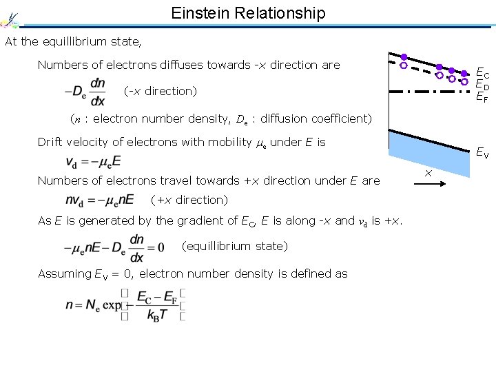
Einstein Relationship At the equillibrium state, Numbers of electrons diffuses towards -x direction are EC ED EF (-x direction) (n : electron number density, De : diffusion coefficient) Drift velocity of electrons with mobility e under E is Numbers of electrons travel towards +x direction under E are (+x direction) As E is generated by the gradient of EC, E is along -x and vd is +x. (equillibrium state) Assuming EV = 0, electron number density is defined as EV x

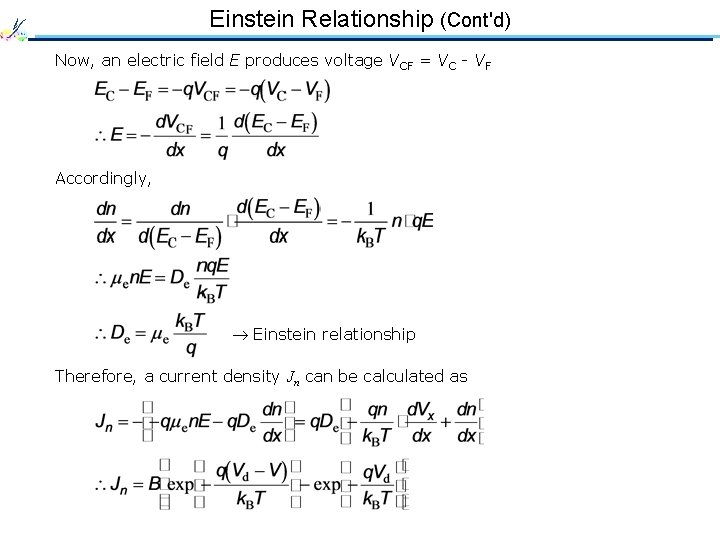
Einstein Relationship (Cont'd) Now, an electric field E produces voltage VCF = VC - VF Accordingly, Einstein relationship Therefore, a current density Jn can be calculated as

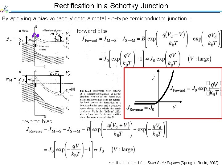
Rectification in a Schottky Junction By applying a bias voltage V onto a metal - n-type semiconductor junction : M - S q(Vd - V) forward bias J V reverse bias * H. Ibach and H. Lüth, Solid-State Physics (Springer, Berlin, 2003).

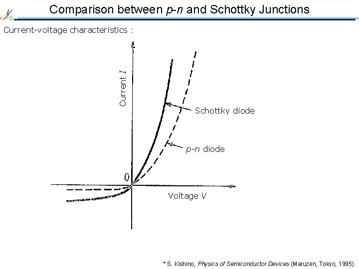
Comparison between p-n and Schottky Junctions Current I Current-voltage characteristics : Schottky diode p-n diode Voltage V * S. Kishino, Physics of Semiconductor Devices (Maruzen, Tokyo, 1995).

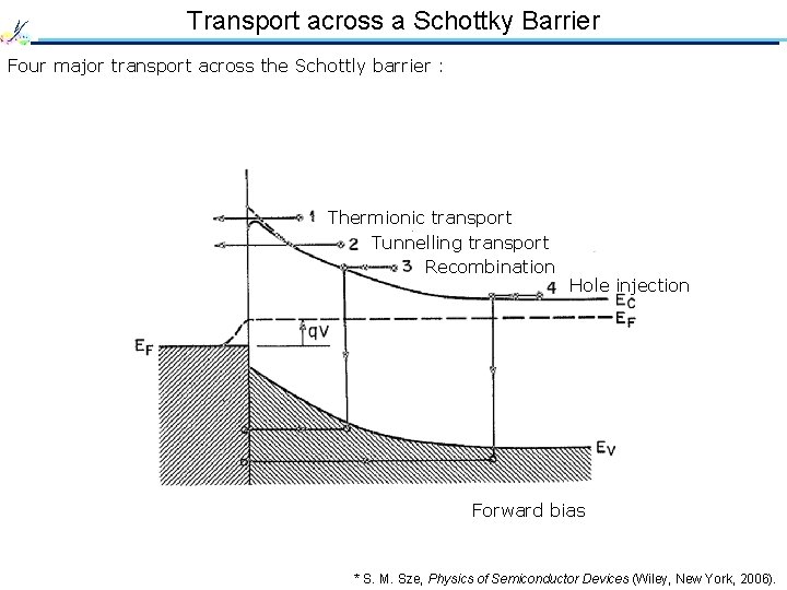
Transport across a Schottky Barrier Four major transport across the Schottly barrier : Thermionic transport Tunnelling transport Recombination Hole injection Forward bias * S. M. Sze, Physics of Semiconductor Devices (Wiley, New York, 2006).

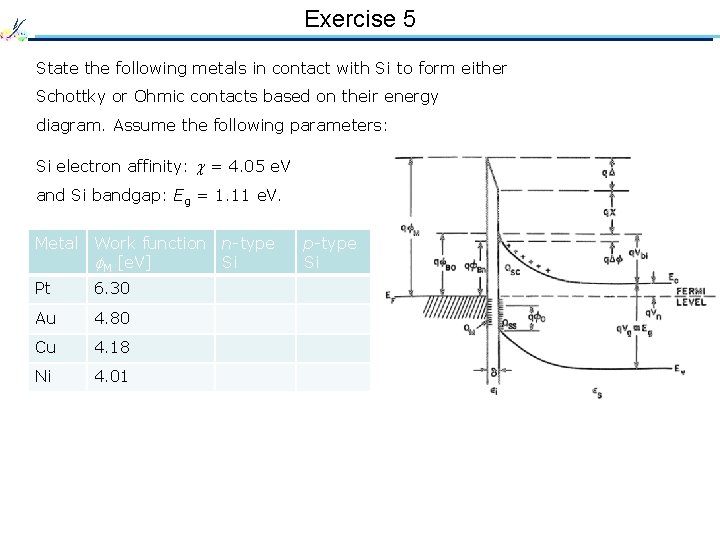
Exercise 5 State the following metals in contact with Si to form either Schottky or Ohmic contacts based on their energy diagram. Assume the following parameters: Si electron affinity: = 4. 05 e. V and Si bandgap: Eg = 1. 11 e. V. Metal Work function n-type M [e. V] Si Pt 6. 30 Au 4. 80 Cu 4. 18 Ni 4. 01 p-type Si