Semiconductor Devices 21 Atsufumi Hirohata Department of Electronics
![Typical Bandgaps between the conduction and valence bands : Bandgap Eg [e. V] Resistivity Typical Bandgaps between the conduction and valence bands : Bandgap Eg [e. V] Resistivity](https://slidetodoc.com/presentation_image_h/a573747ed12be229111d7b38f70de693/image-17.jpg)
- Slides: 27

Semiconductor Devices 21 Atsufumi Hirohata Department of Electronics 11: 00 Thursday, 20/November/2014 (P/T 005)

Contents of Semiconductor Devices Lectures : Atsufumi Hirohata (atsufumi. hirohata@york. ac. uk, P/Z 019) p-n junctions and Schottky diodes (Weeks 8 ~ 10) [11: 00 Mon. (P/L 005), Tue. (P/L 006) & Thu. (P/T 005)] 21. Intrinsic semiconductor 22. Extrinsic semiconductor 23. p-n junction 24. Bias application 25. Metal semiconductor junction 26. Schottky junction 27. Metal oxide semiconductor junction Lecture notes / slides : http: //www-users. york. ac. uk/~ah 566/lectures. html

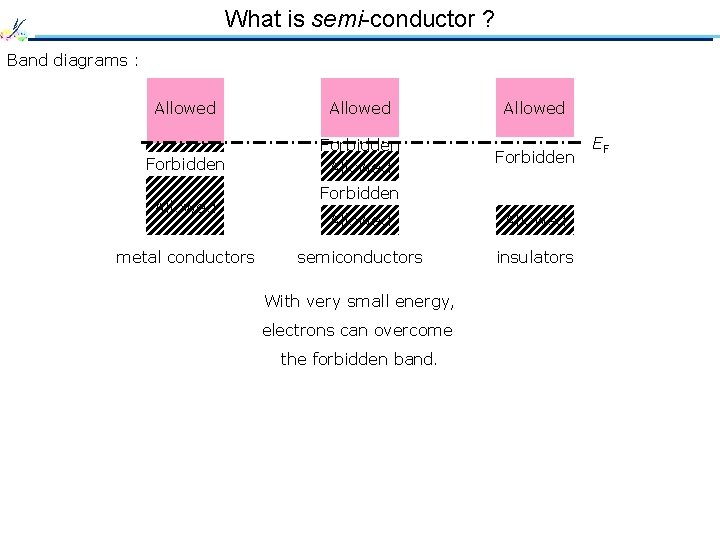
What is semi-conductor ? Band diagrams : Allowed Forbidden Allowed metal conductors Forbidden Allowed semiconductors insulators With very small energy, electrons can overcome the forbidden band. EF

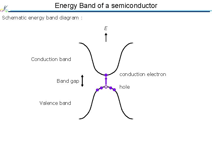
Energy Band of a semiconductor Schematic energy band diagram : E Conduction band conduction electron Band gap hole Valence band

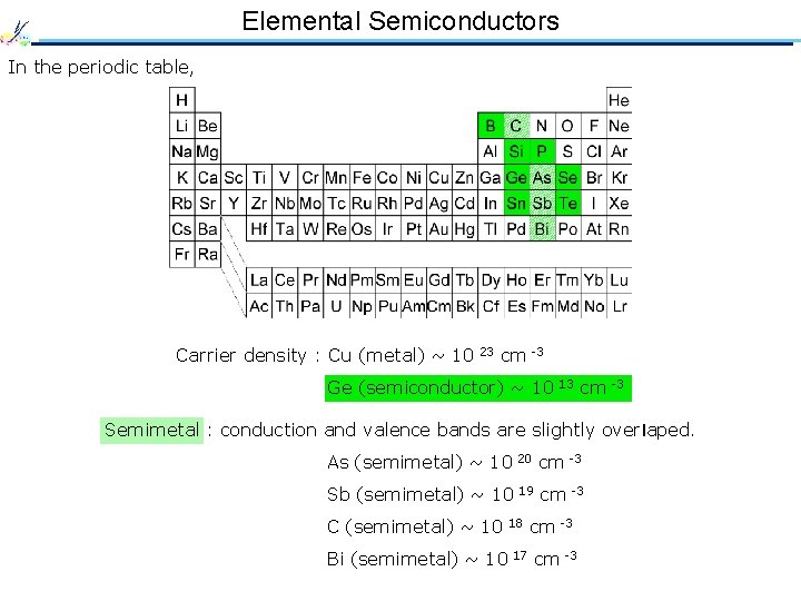
Elemental Semiconductors In the periodic table, Carrier density : Cu (metal) ~ 10 23 cm -3 Ge (semiconductor) ~ 10 13 cm -3 Semimetal : conduction and valence bands are slightly overlaped. As (semimetal) ~ 10 20 cm -3 Sb (semimetal) ~ 10 19 cm -3 C (semimetal) ~ 10 18 cm -3 Bi (semimetal) ~ 10 17 cm -3

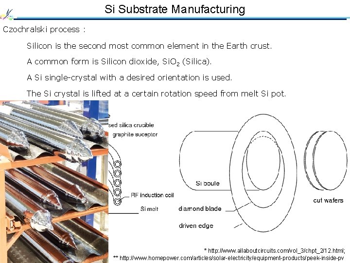
Si Substrate Manufacturing Czochralski process : Silicon is the second most common element in the Earth crust. A common form is Silicon dioxide, Si. O 2 (Silica). A Si single-crystal with a desired orientation is used. The Si crystal is lifted at a certain rotation speed from melt Si pot. * http: //www. allaboutcircuits. com/vol_3/chpt_2/12. html; ** http: //www. homepower. com/articles/solar-electricity/equipment-products/peek-inside-pv

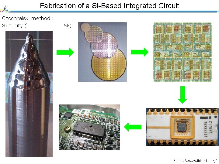
Fabrication of a Si-Based Integrated Circuit Czochralski method : Si purity (99. 99999 %) * http: //www. wikipedia. org/

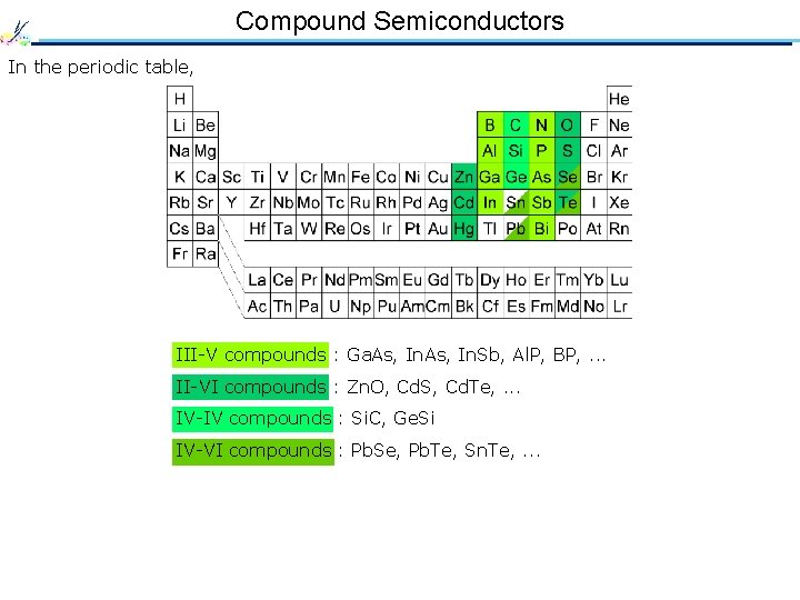
Compound Semiconductors In the periodic table, III-V compounds : Ga. As, In. Sb, Al. P, BP, . . . II-VI compounds : Zn. O, Cd. S, Cd. Te, . . . IV-IV compounds : Si. C, Ge. Si IV-VI compounds : Pb. Se, Pb. Te, Sn. Te, . . .

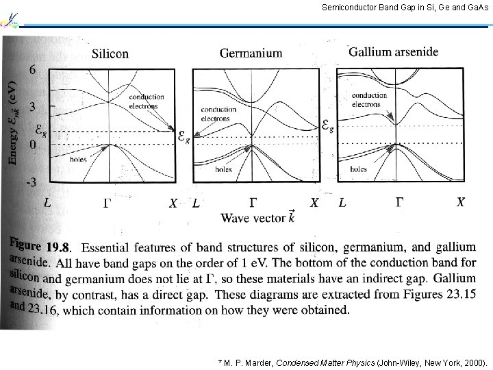
Semiconductor Band Gap in Si, Ge and Ga. As * M. P. Marder, Condensed Matter Physics (John-Wiley, New York, 2000).

21 Intrinsic Semiconductor • Bandgap Conduction band • Valence band • • Fermi level • Shockley Model • Carrier density • Ion implantation

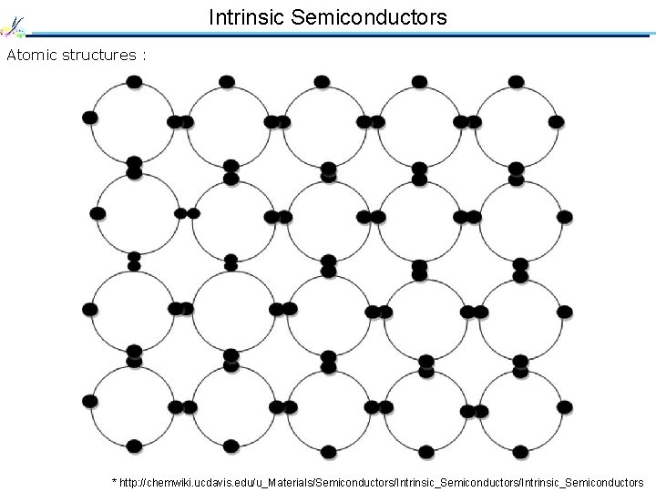
Intrinsic Semiconductors Atomic structures : * http: //chemwiki. ucdavis. edu/u_Materials/Semiconductors/Intrinsic_Semiconductors

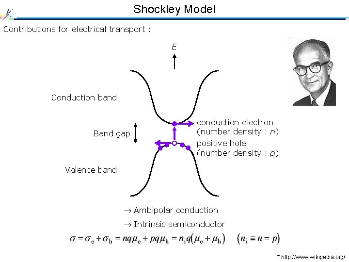
Shockley Model Contributions for electrical transport : E Conduction band Band gap conduction electron (number density : n) positive hole (number density : p) Valence band Ambipolar conduction Intrinsic semiconductor * http: //www. wikipedia. org/

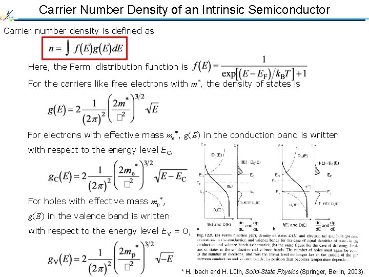
Carrier Number Density of an Intrinsic Semiconductor Carrier number density is defined as Here, the Fermi distribution function is For the carriers like free electrons with m*, the density of states is For electrons with effective mass me*, g(E) in the conduction band is written with respect to the energy level EC, For holes with effective mass mp*, g(E) in the valence band is written with respect to the energy level EV = 0, * H. Ibach and H. Lüth, Solid-State Physics (Springer, Berlin, 2003).

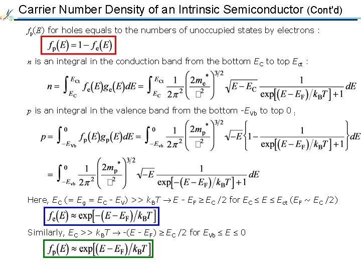
Carrier Number Density of an Intrinsic Semiconductor (Cont'd) fp(E) for holes equals to the numbers of unoccupied states by electrons : n is an integral in the conduction band from the bottom EC to top Ect : p is an integral in the valence band from the bottom -EVb to top 0 : Here, EC (= Eg = EC - EV) >> k. BT E - EF EC /2 for EC E Ect (EF ~ EC /2) Similarly, EC >> k. BT -(E - EF) EC /2 for EVb E 0

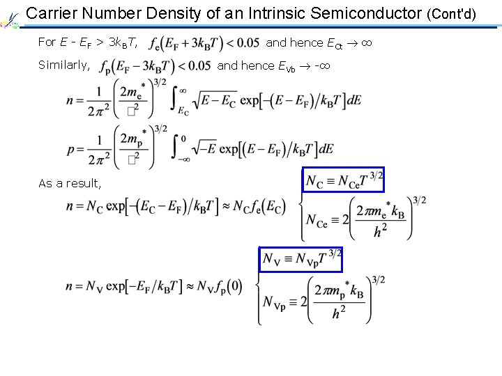
Carrier Number Density of an Intrinsic Semiconductor (Cont'd) For E - EF > 3 k. BT, Similarly, As a result, and hence ECt ∞ and hence EVb -∞

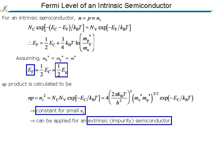
Fermi Level of an Intrinsic Semiconductor For an intrinsic semiconductor, Assuming, me* = mp* = m* np product is calculated to be constant for small ni can be applied for an extrinsic (impurity) semiconductor
![Typical Bandgaps between the conduction and valence bands Bandgap Eg e V Resistivity Typical Bandgaps between the conduction and valence bands : Bandgap Eg [e. V] Resistivity](https://slidetodoc.com/presentation_image_h/a573747ed12be229111d7b38f70de693/image-17.jpg)
Typical Bandgaps between the conduction and valence bands : Bandgap Eg [e. V] Resistivity r [W cm] Ge 0. 66 0. 5 Si 1. 11 2. 3 × 10³ Ga. As 1. 43 ~ 103 C (diamond) 6~7 × 10¹² Eg ∝ r Semiconductors : Eg ~ 0. 1 ~3. 0 e. V

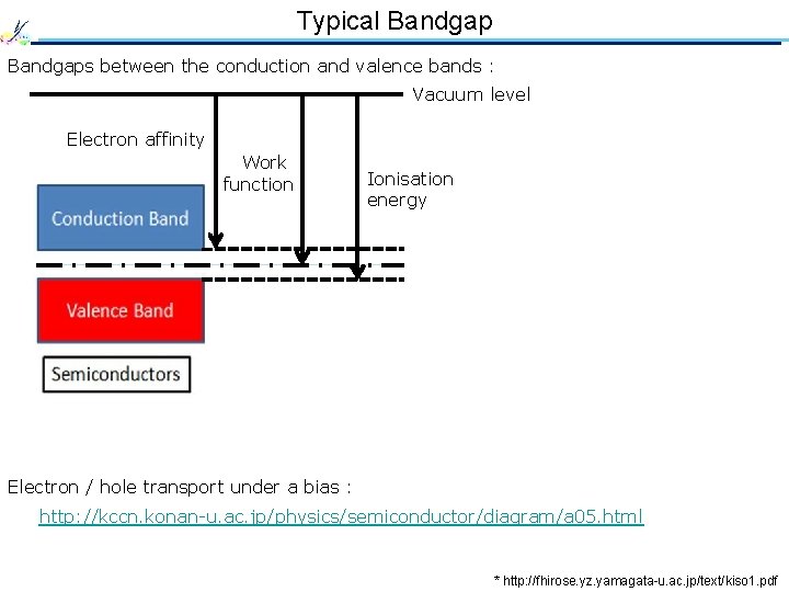
Typical Bandgaps between the conduction and valence bands : Vacuum level Electron affinity Work function Ionisation energy Electron / hole transport under a bias : http: //kccn. konan-u. ac. jp/physics/semiconductor/diagram/a 05. html * http: //fhirose. yz. yamagata-u. ac. jp/text/kiso 1. pdf

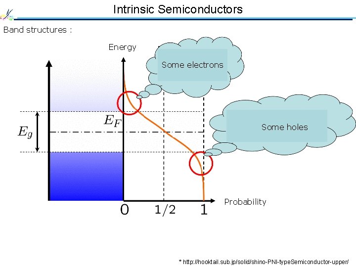
Intrinsic Semiconductors Band structures : Energy Some electrons Some holes Probability * http: //hooktail. sub. jp/solid/shino-PNI-type. Semiconductor-upper/

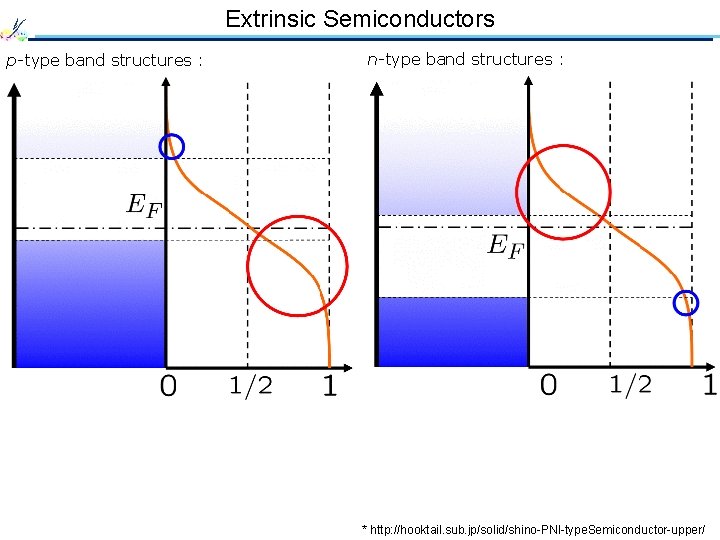
Extrinsic Semiconductors p-type band structures : n-type band structures : * http: //hooktail. sub. jp/solid/shino-PNI-type. Semiconductor-upper/

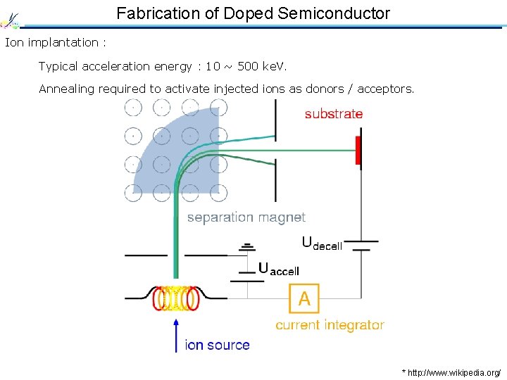
Fabrication of Doped Semiconductor Ion implantation : Typical acceleration energy : 10 ~ 500 ke. V. Annealing required to activate injected ions as donors / acceptors. * http: //www. wikipedia. org/

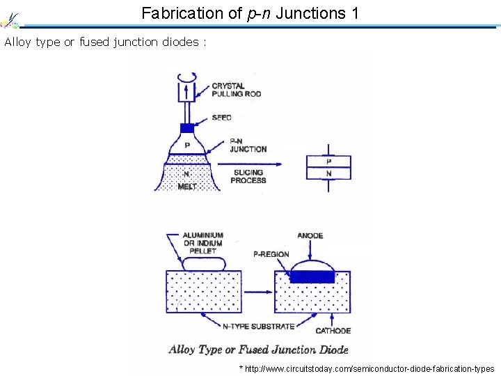
Fabrication of p-n Junctions 1 Alloy type or fused junction diodes : * http: //www. circuitstoday. com/semiconductor-diode-fabrication-types

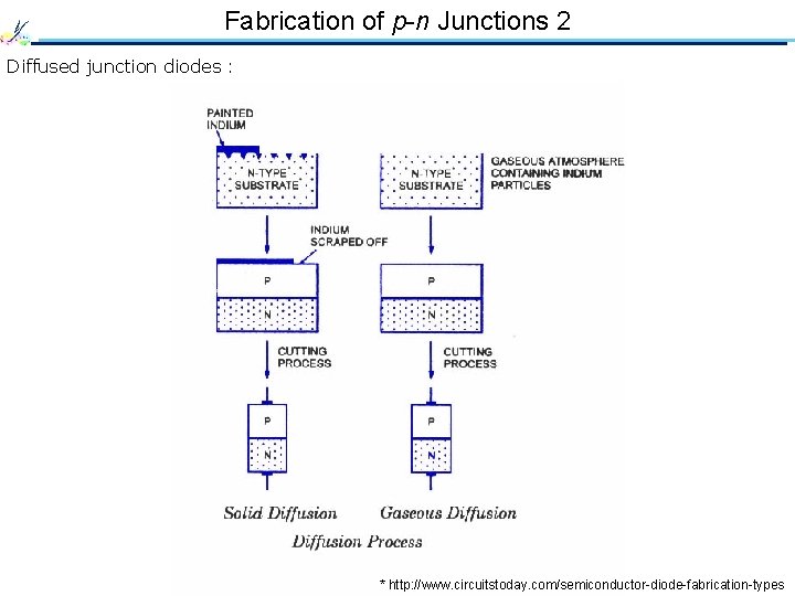
Fabrication of p-n Junctions 2 Diffused junction diodes : * http: //www. circuitstoday. com/semiconductor-diode-fabrication-types

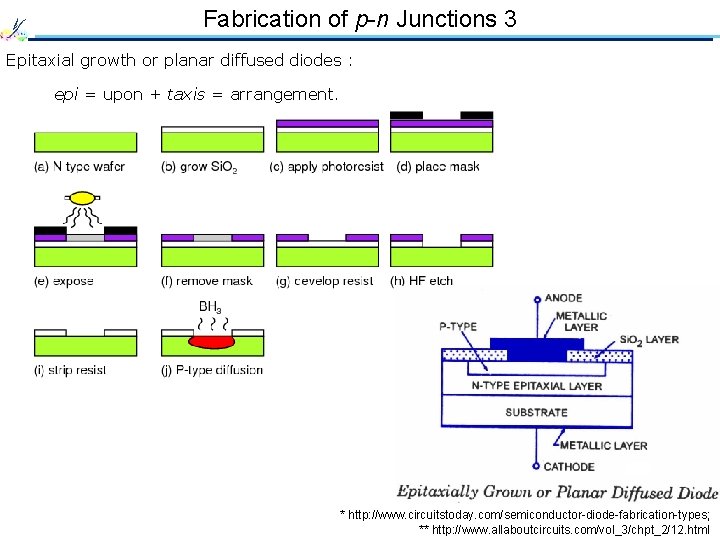
Fabrication of p-n Junctions 3 Epitaxial growth or planar diffused diodes : epi = upon + taxis = arrangement. * http: //www. circuitstoday. com/semiconductor-diode-fabrication-types; ** http: //www. allaboutcircuits. com/vol_3/chpt_2/12. html

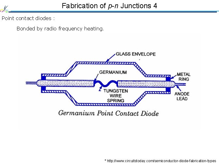
Fabrication of p-n Junctions 4 Point contact diodes : Bonded by radio frequency heating. * http: //www. circuitstoday. com/semiconductor-diode-fabrication-types

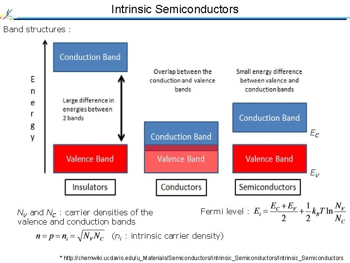
Intrinsic Semiconductors Band structures : EC EV NV and NC : carrier densities of the valence and conduction bands Fermi level : (ni : intrinsic carrier density) * http: //chemwiki. ucdavis. edu/u_Materials/Semiconductors/Intrinsic_Semiconductors

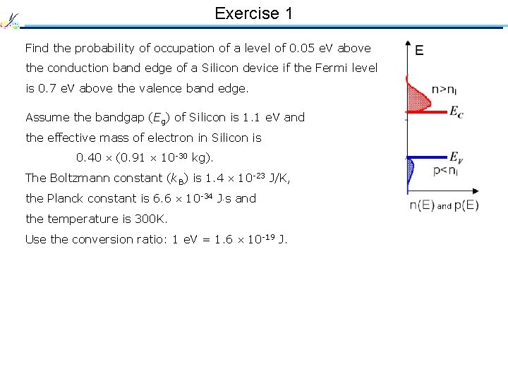
Exercise 1 Find the probability of occupation of a level of 0. 05 e. V above the conduction band edge of a Silicon device if the Fermi level is 0. 7 e. V above the valence band edge. Assume the bandgap (Eg) of Silicon is 1. 1 e. V and the effective mass of electron in Silicon is 0. 40 (0. 91 10 -30 kg). The Boltzmann constant (k. B) is 1. 4 10 -23 J/K, the Planck constant is 6. 6 10 -34 J s and the temperature is 300 K. Use the conversion ratio: 1 e. V = 1. 6 10 -19 J.