Semiconductor Devices 22 Atsufumi Hirohata Department of Electronics
- Slides: 18

Semiconductor Devices 22 Atsufumi Hirohata Department of Electronics 11: 00 Monday, 24/November/2014 (P/L 005)

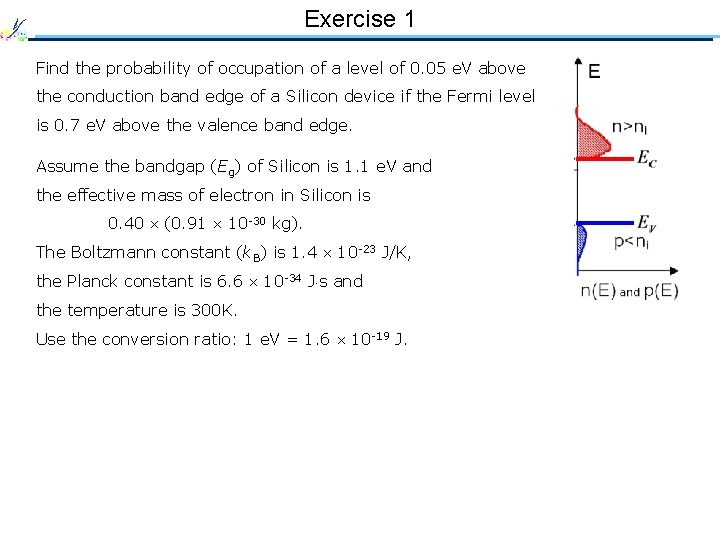
Exercise 1 Find the probability of occupation of a level of 0. 05 e. V above the conduction band edge of a Silicon device if the Fermi level is 0. 7 e. V above the valence band edge. Assume the bandgap (Eg) of Silicon is 1. 1 e. V and the effective mass of electron in Silicon is 0. 40 (0. 91 10 -30 kg). The Boltzmann constant (k. B) is 1. 4 10 -23 J/K, the Planck constant is 6. 6 10 -34 J s and the temperature is 300 K. Use the conversion ratio: 1 e. V = 1. 6 10 -19 J.

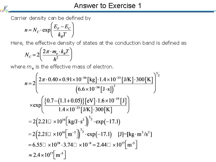
Answer to Exercise 1 Carrier density can be defined by Here, the effective density of states at the conduction band is defined as where me is the effective mass of electron.

22 Extrinsic Semiconductor • Doping Donor / acceptor • • Carrier density

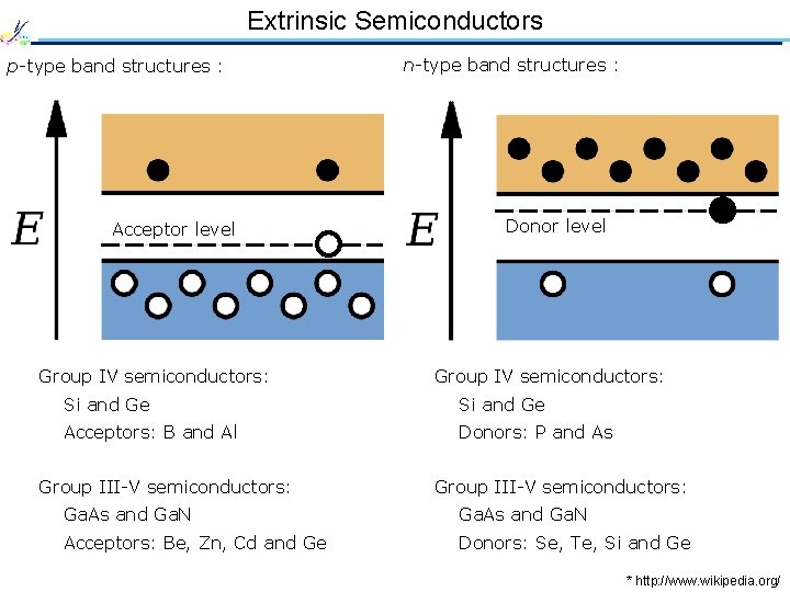
Extrinsic Semiconductors p-type band structures : Acceptor level Group IV semiconductors: n-type band structures : Donor level Group IV semiconductors: Si and Ge Acceptors: B and Al Donors: P and As Group III-V semiconductors: Ga. As and Ga. N Acceptors: Be, Zn, Cd and Ge Donors: Se, Te, Si and Ge * http: //www. wikipedia. org/

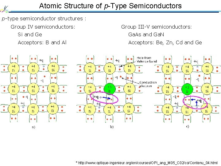
Atomic Structure of p-Type Semiconductors p-type semiconductor structures : Group IV semiconductors: Group III-V semiconductors: Si and Ge Ga. As and Ga. N Acceptors: B and Al Acceptors: Be, Zn, Cd and Ge * http: //www. optique-ingenieur. org/en/courses/OPI_ang_M 05_C 02/co/Contenu_04. html

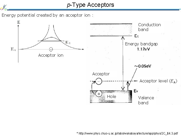
p-Type Acceptors Energy potential created by an acceptor ion : Conduction band Energy bandgap Acceptor ion Acceptor level (EA) Hole Valence band * http: //www. phys. chuo-u. ac. jp/labs/wakabaya/lecture/applphys/2 C_$4. 3. pdf

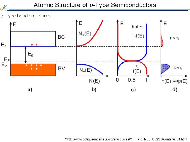
Atomic Structure of p-Type Semiconductors p-type band structures : * http: //www. optique-ingenieur. org/en/courses/OPI_ang_M 05_C 02/co/Contenu_04. html

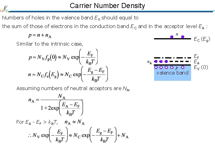
Carrier Number Density Numbers of holes in the valence band EV should equal to the sum of those of electrons in the conduction band EC and in the acceptor level EA : n Similar to the intrinsic case, n. A Assuming numbers of neutral acceptors are NA, For EA - EF > k. BT, p valence band EC (Eg) EF EA EV (0)

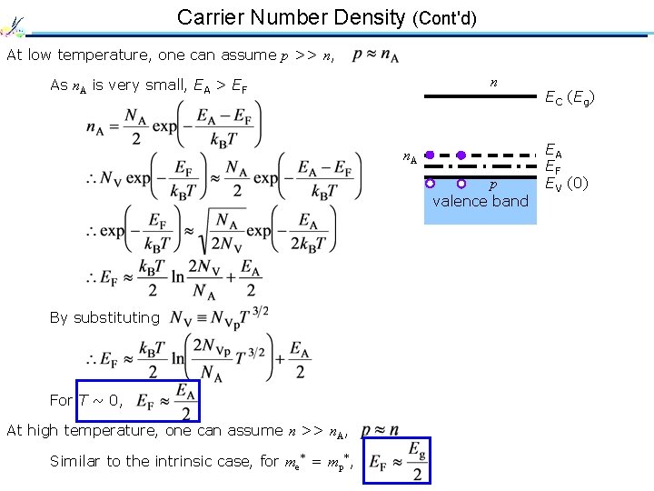
Carrier Number Density (Cont'd) At low temperature, one can assume p >> n, n As n. A is very small, EA > EF n. A p valence band By substituting For T ~ 0, At high temperature, one can assume n >> n. A, Similar to the intrinsic case, for me* = mp*, EC (Eg) EA EF EV (0)

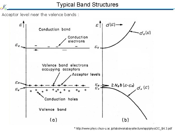
Typical Band Structures Acceptor level near the valence bands : * http: //www. phys. chuo-u. ac. jp/labs/wakabaya/lecture/applphys/2 C_$4. 3. pdf

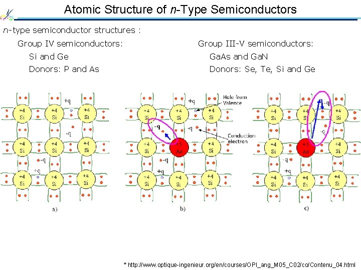
Atomic Structure of n-Type Semiconductors n-type semiconductor structures : Group IV semiconductors: Group III-V semiconductors: Si and Ge Ga. As and Ga. N Donors: P and As Donors: Se, Te, Si and Ge * http: //www. optique-ingenieur. org/en/courses/OPI_ang_M 05_C 02/co/Contenu_04. html

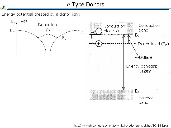
n-Type Donors Energy potential created by a donor ion : Donor ion Conduction electron Conduction band Donor level (ED) Energy bandgap Valence band * http: //www. phys. chuo-u. ac. jp/labs/wakabaya/lecture/applphys/2 C_$4. 3. pdf

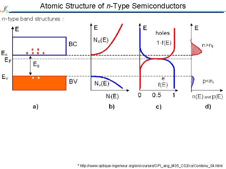
Atomic Structure of n-Type Semiconductors n-type band structures : * http: //www. optique-ingenieur. org/en/courses/OPI_ang_M 05_C 02/co/Contenu_04. html

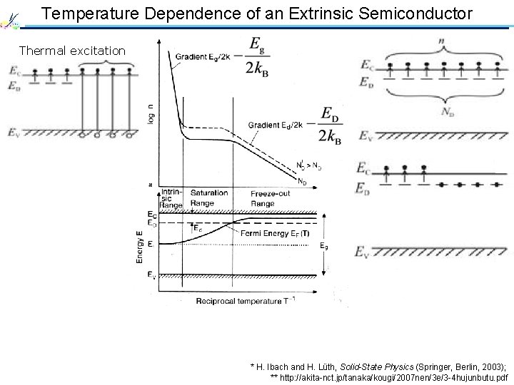
Temperature Dependence of an Extrinsic Semiconductor Thermal excitation * H. Ibach and H. Lüth, Solid-State Physics (Springer, Berlin, 2003); ** http: //akita-nct. jp/tanaka/kougi/2007 nen/3 e/3 -4 hujunbutu. pdf

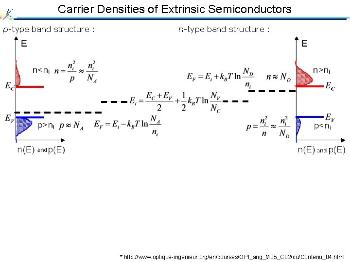
Carrier Densities of Extrinsic Semiconductors p-type band structure : n-type band structure : * http: //www. optique-ingenieur. org/en/courses/OPI_ang_M 05_C 02/co/Contenu_04. html

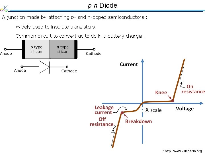
p-n Diode A junction made by attaching p- and n-doped semiconductors : Widely used to insulate transistors. Common circuit to convert ac to dc in a battery charger. * http: //www. wikipedia. org/

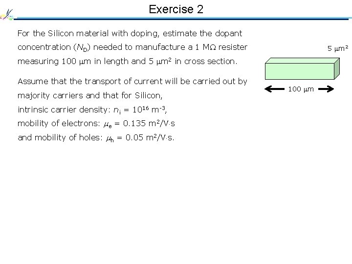
Exercise 2 For the Silicon material with doping, estimate the dopant concentration (ND) needed to manufacture a 1 MW resister 5 mm 2 measuring 100 mm in length and 5 mm 2 in cross section. Assume that the transport of current will be carried out by majority carriers and that for Silicon, intrinsic carrier density: ni = 1016 m-3, mobility of electrons: me = 0. 135 m 2/V s and mobility of holes: mh = 0. 05 m 2/V s. 100 mm