Semiconductor Devices 24 Atsufumi Hirohata Department of Electronics

- Slides: 19

Semiconductor Devices 24 Atsufumi Hirohata Department of Electronics 11: 00 Thursday, 27/November/2014 (P/T 005)

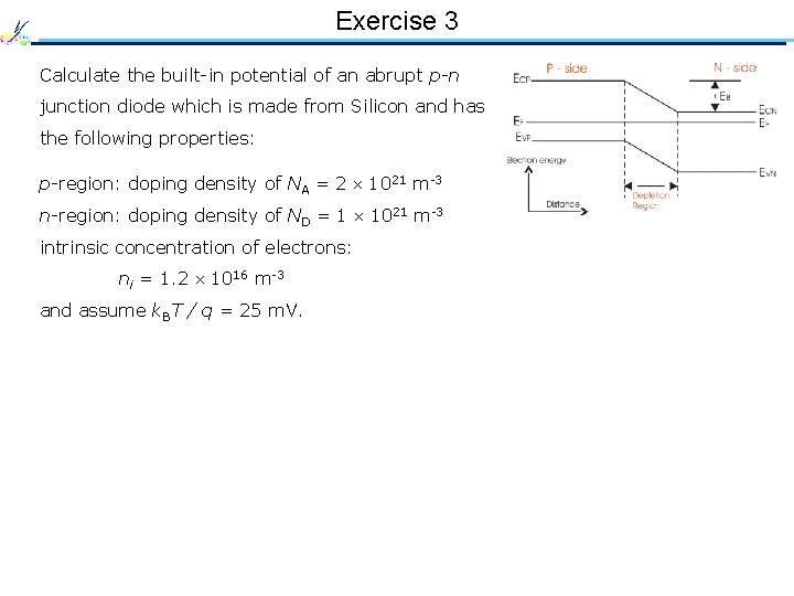
Exercise 3 Calculate the built-in potential of an abrupt p-n junction diode which is made from Silicon and has the following properties: p-region: doping density of NA = 2 1021 m-3 n-region: doping density of ND = 1 1021 m-3 intrinsic concentration of electrons: ni = 1. 2 1016 m-3 and assume k. BT / q = 25 m. V.

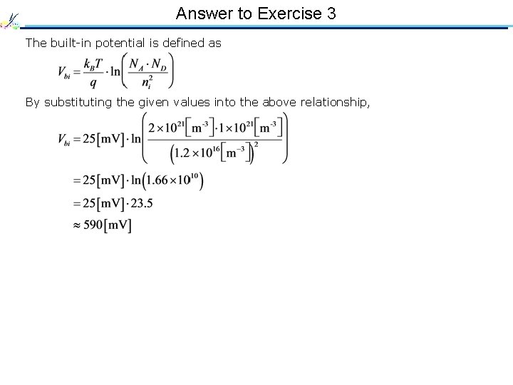
Answer to Exercise 3 The built-in potential is defined as By substituting the given values into the above relationship,

24 Bias Application • Forward bias • Reverse bias • Current rectification • Junction breakdown

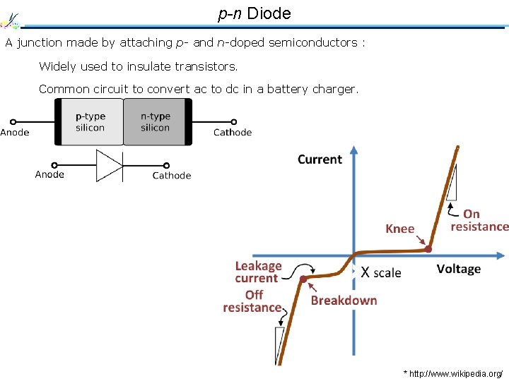
p-n Diode A junction made by attaching p- and n-doped semiconductors : Widely used to insulate transistors. Common circuit to convert ac to dc in a battery charger. * http: //www. wikipedia. org/

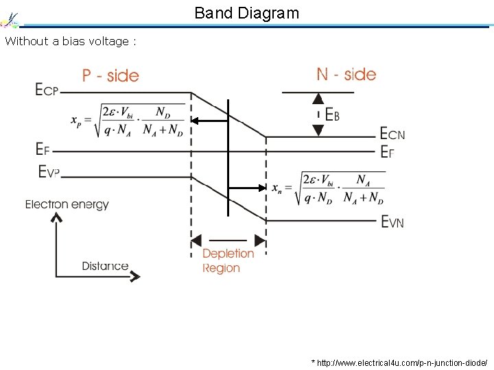
Band Diagram Without a bias voltage : * http: //www. electrical 4 u. com/p-n-junction-diode/

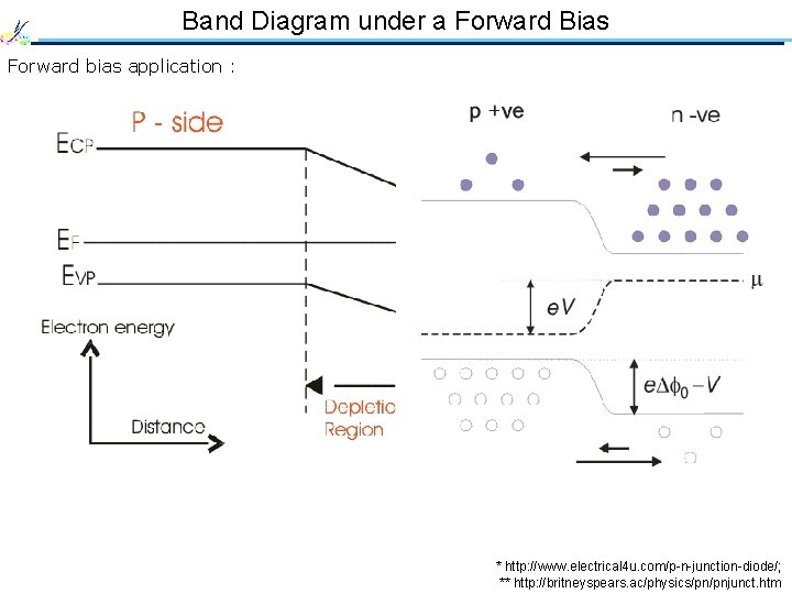
Band Diagram under a Forward Bias Forward bias application : * http: //www. electrical 4 u. com/p-n-junction-diode/; ** http: //britneyspears. ac/physics/pn/pnjunct. htm

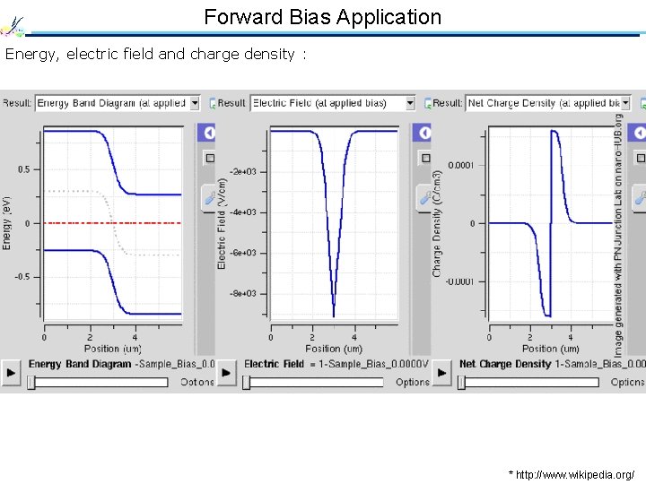
Forward Bias Application Energy, electric field and charge density : * http: //www. wikipedia. org/

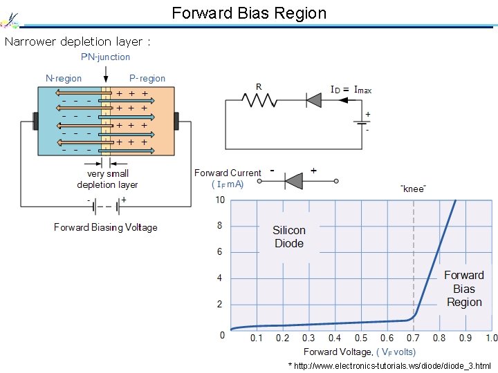
Forward Bias Region Narrower depletion layer : * http: //www. electronics-tutorials. ws/diode_3. html

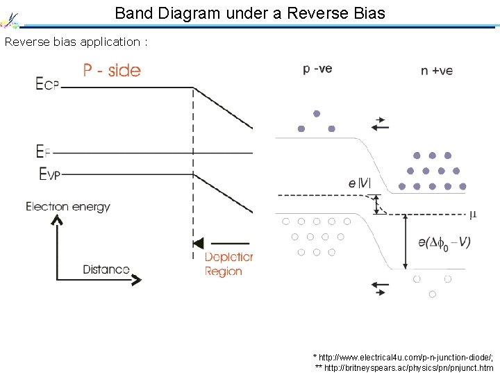
Band Diagram under a Reverse Bias Reverse bias application : * http: //www. electrical 4 u. com/p-n-junction-diode/; ** http: //britneyspears. ac/physics/pn/pnjunct. htm

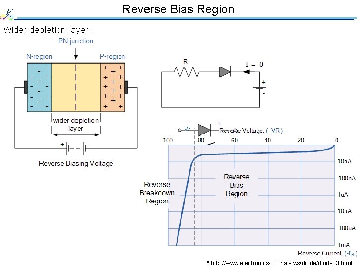
Reverse Bias Region Wider depletion layer : * http: //www. electronics-tutorials. ws/diode_3. html

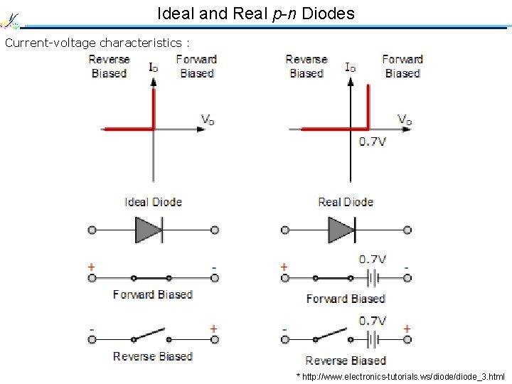
Ideal and Real p-n Diodes Current-voltage characteristics : * http: //www. electronics-tutorials. ws/diode_3. html

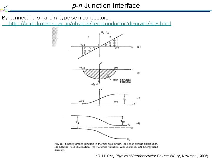
p-n Junction Interface By connecting p- and n-type semiconductors, http: //kccn. konan-u. ac. jp/physics/semiconductor/diagram/a 08. html * S. M. Sze, Physics of Semiconductor Devices (Wiley, New York, 2006).

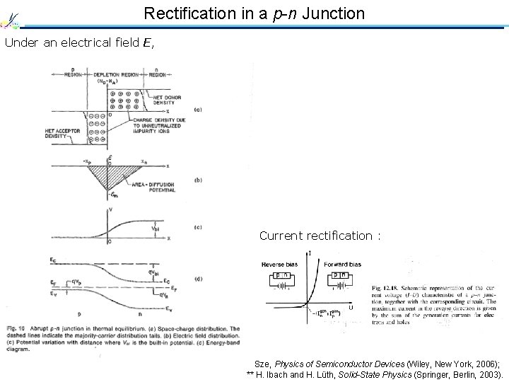
Rectification in a p-n Junction Under an electrical field E, Current rectification : * S. M. Sze, Physics of Semiconductor Devices (Wiley, New York, 2006); ** H. Ibach and H. Lüth, Solid-State Physics (Springer, Berlin, 2003).

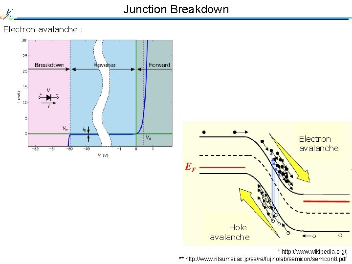
Junction Breakdown Electron avalanche : Electron avalanche Hole avalanche * http: //www. wikipedia. org/; ** http: //www. ritsumei. ac. jp/se/re/fujinolab/semicon 8. pdf

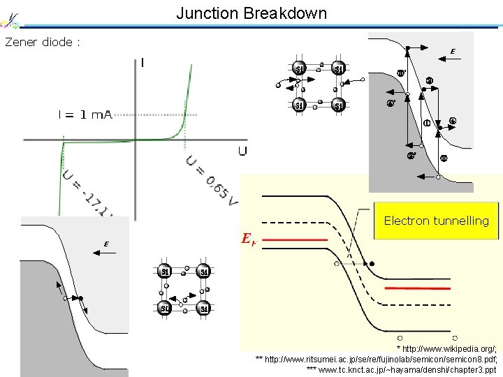
Junction Breakdown Zener diode : E Si Si ③' ② Si Si ④' ④ ① ②' ③ Electron tunnelling E Si Si * http: //www. wikipedia. org/; ** http: //www. ritsumei. ac. jp/se/re/fujinolab/semicon 8. pdf; *** www. tc. knct. ac. jp/~hayama/denshi/chapter 3. ppt

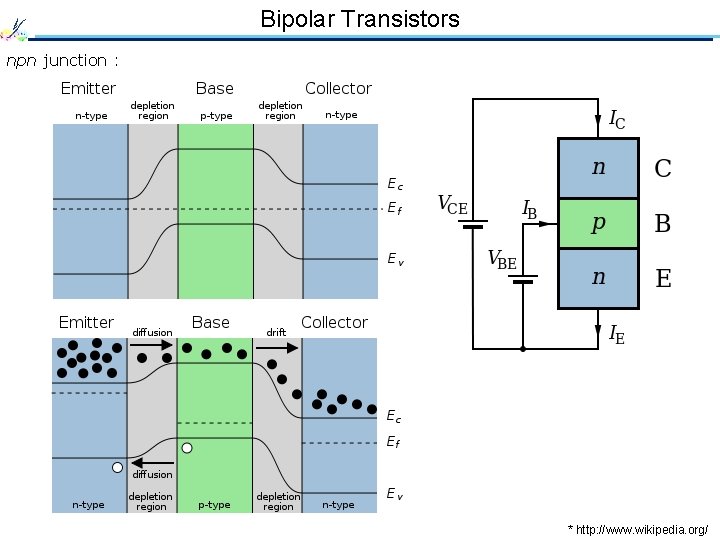
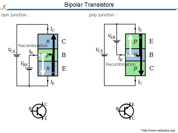
Bipolar Transistors npn junction : * http: //www. wikipedia. org/

Bipolar Transistors pnp junction : npn junction : e Recombination h h Recombination e * http: //www. wikipedia. org/

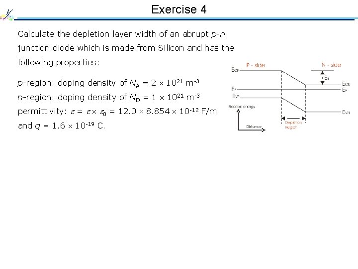
Exercise 4 Calculate the depletion layer width of an abrupt p-n junction diode which is made from Silicon and has the following properties: p-region: doping density of NA = 2 1021 m-3 n-region: doping density of ND = 1 1021 m-3 permittivity: e = e e 0 = 12. 0 8. 854 10 -12 F/m and q = 1. 6 10 -19 C.