Information Storage and Spintronics 01 Atsufumi Hirohata Department

- Slides: 25

Information Storage and Spintronics 01 Atsufumi Hirohata Department of Electronic Engineering 13: 30 Monday, 05/October/2020 (B/B 006 & online) & 12: 00 Thursday, 08/October/2020 (online)

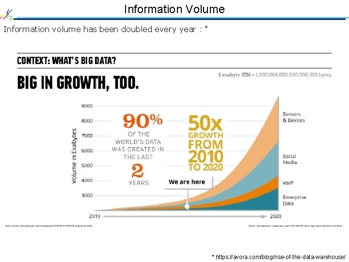
Information Volume Information volume has been doubled every year : * * https: //avora. com/blog/rise-of-the-data-warehouse/

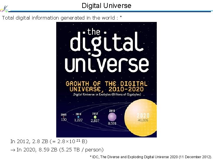
Digital Universe Total digital information generated in the world : * In 2012, 2. 8 ZB (= 2. 8× 10 21 B) In 2020, 8. 59 ZB (5. 25 TB / person) * IDC, The Diverse and Exploding Digital Universe 2020 (11 December 2012).

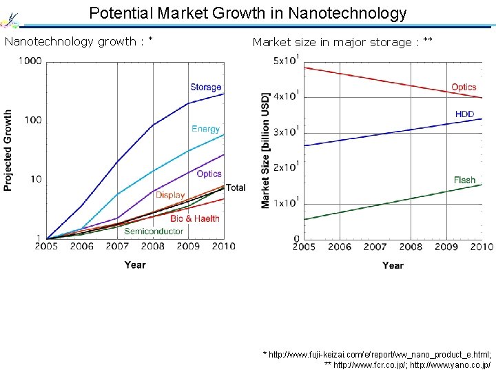
Potential Market Growth in Nanotechnology growth : * Market size in major storage : ** * http: //www. fuji-keizai. com/e/report/ww_nano_product_e. html; ** http: //www. fcr. co. jp/; http: //www. yano. co. jp/

Contents of Information Storage and Spintronics Lectures : Atsufumi Hirohata (atsufumi. hirohata@york. ac. uk, P/Z 019) Advancement in information storages and spintronics (Weeks 2 ~ 9) All lectures will be uploaded weekly in advance at http: //www-users. york. ac. uk/~ah 566/lectures. html 13: 30 ~ 14: 30 Mons. (B/B 006 & online – Zoom) 12: 00 ~ 13: 00 Thus. (online – Zoom) I. Introduction to information storage (01 & 02) II. Magnetic information storages (03 ~ 06) III. Solid-state information storages (07 ~ 11) IV. Spintronic devices (12 ~ 18) Practicals : Analysis on a spintronic device using XRD, VSM, MFM and MR (Weeks 3 ~ 8) Operation, data and instruction will be uploaded weekly in advance at http: //www-users. york. ac. uk/~ah 566/lectures. html 09: 00 ~ 11: 00 Weds. (online – Zoom) Continuous Assessment : Assignment to be submitted via VLE (Week 10).

References Magnetic storages : - S. X. Wang and A. M. Taratorin, Magnetic Information Storage Technology (Academic Press, New York, 1999). - C. D. Mee and E. D. Daniel, Magnetic Recording (Mc. Graw Hill, New York, 1996). Semiconductor storages : - D. Richter, Flash Memories: Economic Principles of Performance, Cost and Reliability Optimization (Springer, Berlin, 2013). - J. Brewer and M. Gill, Nonvolatile Memory Technologies with Emphasis on Flash: A Comprehensive Guide to Understanding and Using Flash Memory Devices (Wiley-Blackwell, New York, 2008). Spintronics : - A. Hirohata and K. Takanashi, J. Phys. D: Appl. Phys. 47, 193001 (2014). - A. Hirohata et al. , J. Magn. Mater. 509, 166711 (2020). Lecture notes / slides : http: //www-users. york. ac. uk/~ah 566/lectures. html Q & A : Slack page as invited

01 Principles of Information Storage • Moore’s law • Information storage • Von Neumann’s model • Internal connections • Memory access • Bit and byte

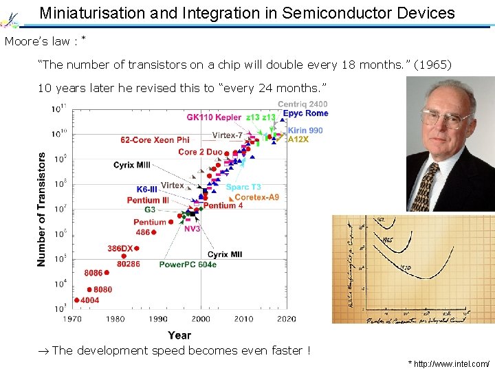
Miniaturisation and Integration in Semiconductor Devices Moore’s law : * “The number of transistors on a chip will double every 18 months. ” (1965) 10 years later he revised this to “every 24 months. ” The development speed becomes even faster ! * http: //www. intel. com/

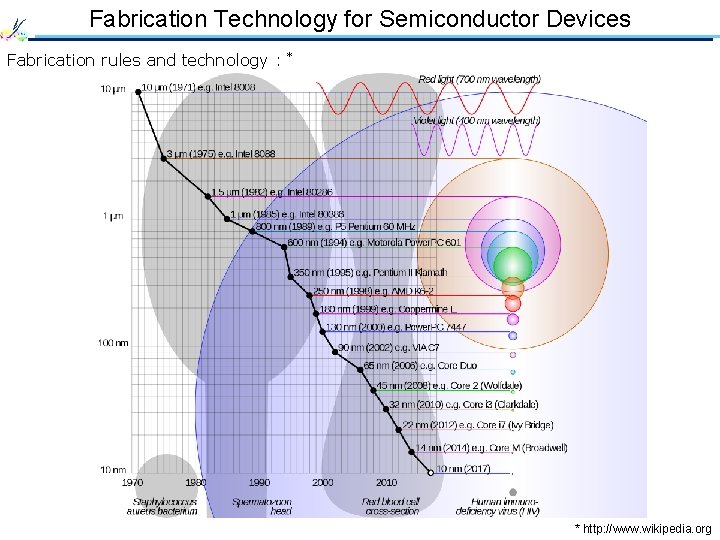
Fabrication Technology for Semiconductor Devices Fabrication rules and technology : * * http: //www. wikipedia. org

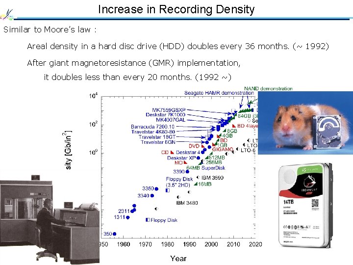
Increase in Recording Density Similar to Moore’s law : Areal density in a hard disc drive (HDD) doubles every 36 months. (~ 1992) After giant magnetoresistance (GMR) implementation, it doubles less than every 20 months. (1992 ~)

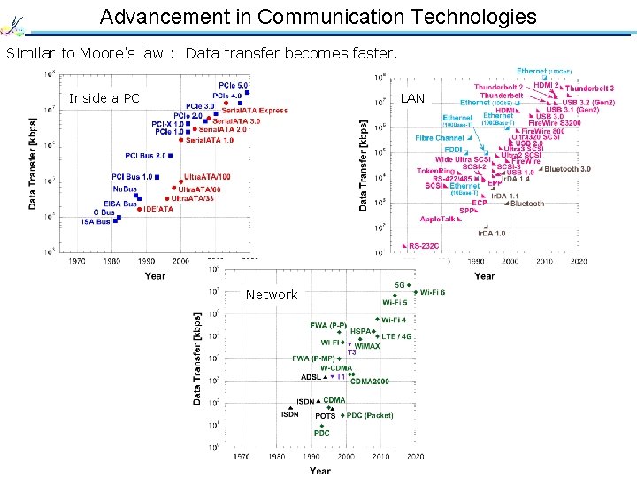
Advancement in Communication Technologies Similar to Moore’s law : Data transfer becomes faster. Inside a PC LAN Network

Can We Continue Such Trends ? Further miniaturisation is too expensive : * https: //www. industryweek. com/emerging-technologies/globalfoundries-gives-advanced-chip-production-technology ** https: //9 to 5 mac. com/2018/06/21/tsmc-5 nm-process-plant/amp/

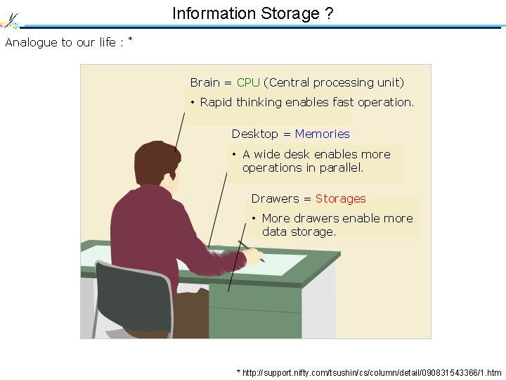
Information Storage ? Analogue to our life : * Brain = CPU (Central processing unit) • Rapid thinking enables fast operation. Desktop = Memories • A wide desk enables more operations in parallel. Drawers = Storages • More drawers enable more data storage. * http: //support. nifty. com/tsushin/cs/column/detail/090831543366/1. htm

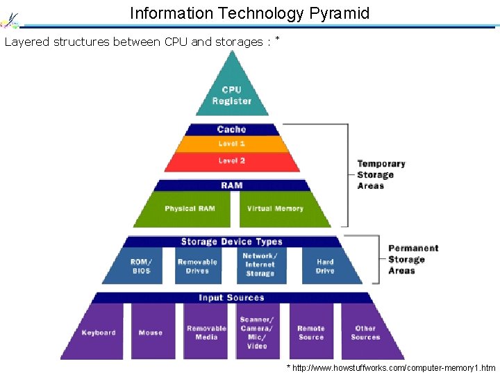
Information Technology Pyramid Layered structures between CPU and storages : * * http: //www. howstuffworks. com/computer-memory 1. htm

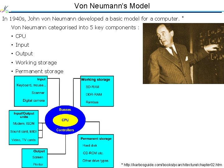
Von Neumann’s Model In 1940 s, John von Neumann developed a basic model for a computer. * Von Neumann categorised into 5 key components : • CPU • Input • Output • Working storage • Permanent storage * http: //karbosguide. com/books/pcarchitecture/chapter 02. htm

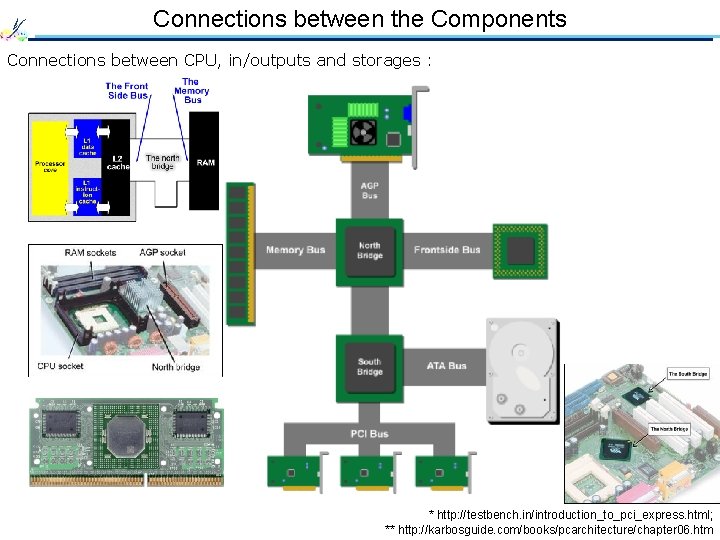
Connections between the Components Connections between CPU, in/outputs and storages : * http: //testbench. in/introduction_to_pci_express. html; ** http: //karbosguide. com/books/pcarchitecture/chapter 06. htm

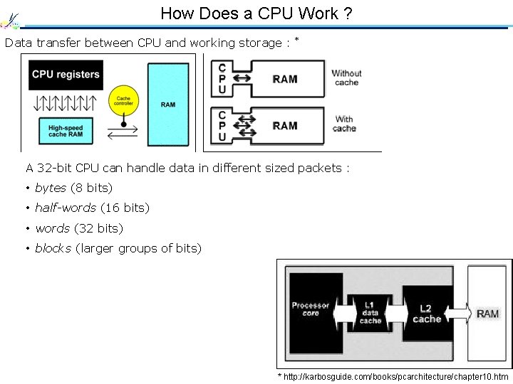
How Does a CPU Work ? Data transfer between CPU and working storage : * A 32 -bit CPU can handle data in different sized packets : • bytes (8 bits) • half-words (16 bits) • words (32 bits) • blocks (larger groups of bits) * http: //karbosguide. com/books/pcarchitecture/chapter 10. htm

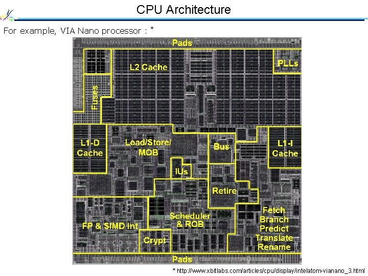
CPU Architecture For example, VIA Nano processor : * * http: //www. xbitlabs. com/articles/cpu/display/intelatom-vianano_3. html

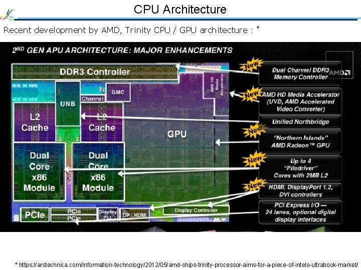
CPU Architecture Recent development by AMD, Trinity CPU / GPU architecture : * * https: //arstechnica. com/information-technology/2012/05/amd-ships-trinity-processor-aims-for-a-piece-of-intels-ultrabook-market/

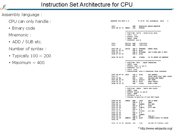
Instruction Set Architecture for CPU Assembly language : CPU can only handle : • Binary code Mnemonic : • ADD / SUB etc. Number of syntax : • Typically 100 ~ 200 • Maximum ~ 400 * http: //www. wikipedia. org/

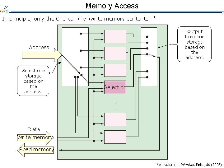
Memory Access In principle, only the CPU can (re-)write memory contents : * Output from one storage based on the address. Address Select one storage based on the address. Selection Data Write memory Read memory * A. Nalamori, Interface Feb. , 44 (2006).

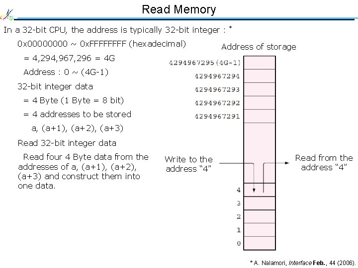
Read Memory In a 32 -bit CPU, the address is typically 32 -bit integer : * 0 x 0000 ~ 0 x. FFFF (hexadecimal) Address of storage = 4, 294, 967, 296 = 4 G Address : 0 ~ (4 G-1) 32 -bit integer data = 4 Byte (1 Byte = 8 bit) = 4 addresses to be stored a, (a+1), (a+2), (a+3) Read 32 -bit integer data Read four 4 Byte data from the addresses of a, (a+1), (a+2), (a+3) and construct them into one data. Write to the address “ 4” Read from the address “ 4” * A. Nalamori, Interface Feb. , 44 (2006).

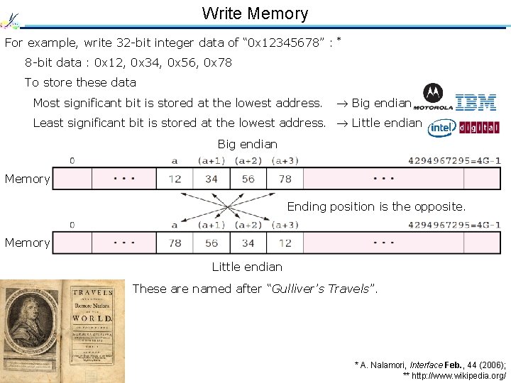
Write Memory For example, write 32 -bit integer data of “ 0 x 12345678” : * 8 -bit data : 0 x 12, 0 x 34, 0 x 56, 0 x 78 To store these data Most significant bit is stored at the lowest address. Big endian Least significant bit is stored at the lowest address. Little endian Big endian Memory Ending position is the opposite. Memory Little endian These are named after “Gulliver’s Travels”. * A. Nalamori, Interface Feb. , 44 (2006); ** http: //www. wikipedia. org/

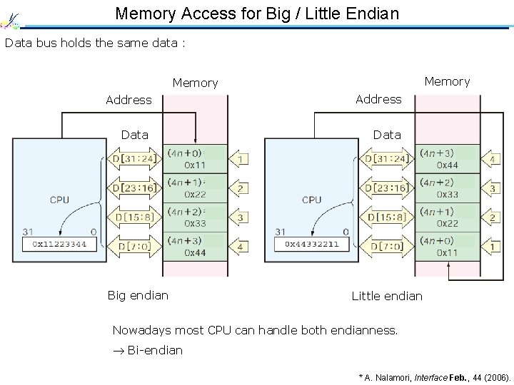
Memory Access for Big / Little Endian Data bus holds the same data : Memory Address Data Big endian Little endian Nowadays most CPU can handle both endianness. Bi-endian * A. Nalamori, Interface Feb. , 44 (2006).

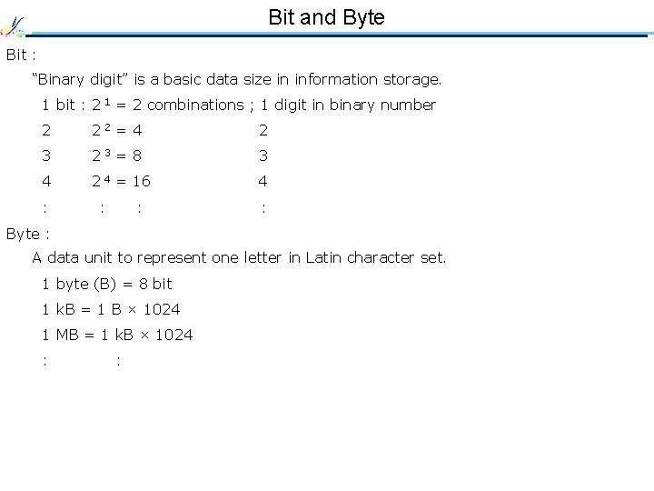
Bit and Byte Bit : “Binary digit” is a basic data size in information storage. 1 bit : 2 1 = 2 combinations ; 1 digit in binary number 2 22 = 4 2 3 23 = 8 3 4 2 4 = 16 4 : : Byte : A data unit to represent one letter in Latin character set. 1 byte (B) = 8 bit 1 k. B = 1 B × 1024 1 MB = 1 k. B × 1024 : :