Information Storage and Spintronics 16 Atsufumi Hirohata Department
- Slides: 22

Information Storage and Spintronics 16 Atsufumi Hirohata Department of Electronic Engineering 13: 30 Monday, 23/November/2020 (B/B 006 & online) & 12: 00 Thursday, 26/November/2020 (online)

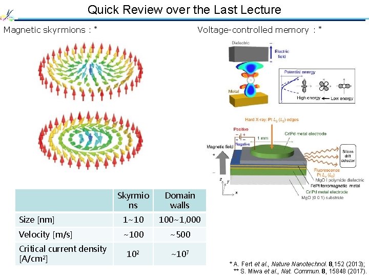
Quick Review over the Last Lecture Magnetic skyrmions : * Voltage-controlled memory : * Skyrmio ns Domain walls Size [nm] 1~10 100~1, 000 Velocity [m/s] ~100 ~500 102 ~107 Critical current density [A/cm 2] * A. Fert et al. , Nature Nanotechnol. 8, 152 (2013); ** S. Miwa et al. , Nat. Commun. 8, 15848 (2017).

16 Three-Terminal Devices • Spin-polarised transistors • Lateral spin-valves • Spin injection • Spin accumulation • Johnson transistors

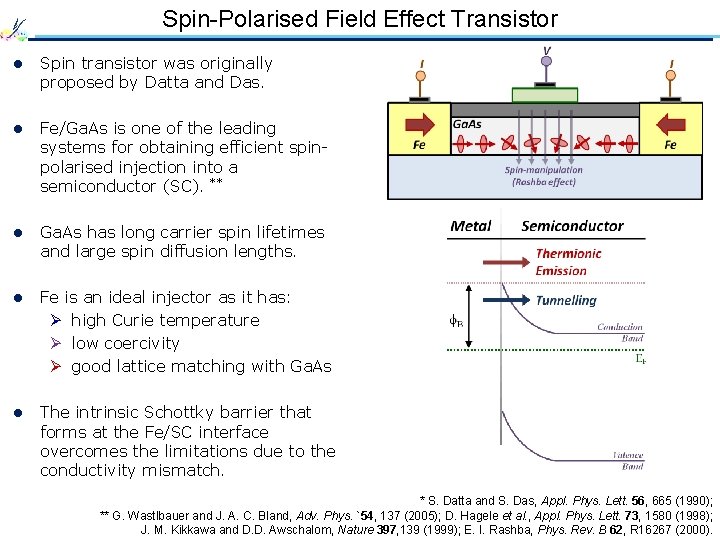
Spin-Polarised Field Effect Transistor l Spin transistor was originally proposed by Datta and Das. l Fe/Ga. As is one of the leading systems for obtaining efficient spinpolarised injection into a semiconductor (SC). ** l Ga. As has long carrier spin lifetimes and large spin diffusion lengths. l Fe is an ideal injector as it has: Ø high Curie temperature Ø low coercivity Ø good lattice matching with Ga. As l The intrinsic Schottky barrier that forms at the Fe/SC interface overcomes the limitations due to the conductivity mismatch. * S. Datta and S. Das, Appl. Phys. Lett. 56, 665 (1990); ** G. Wastlbauer and J. A. C. Bland, Adv. Phys. `54, 137 (2005); D. Hagele et al. , Appl. Phys. Lett. 73, 1580 (1998); J. M. Kikkawa and D. D. Awschalom, Nature 397, 139 (1999); E. I. Rashba, Phys. Rev. B 62, R 16267 (2000).

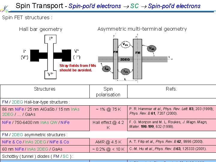
Spin Transport - Spin-pol'd electrons SC Spin-pol'd electrons Spin FET structures : Asymmetric multi-terminal geometry Hall bar geometry Stray fields from FMs should be avoided. Structures Spin polarisation Refs. ~ 1% @ 75 K P. R. Hammar et al. , Phys. Rev. Lett. 83, 203 (1999); Phys. Rev. B 61, 7207 (2000). FM / 2 DEG Hall-bar-type structures : 86 nm Ni. Fe / 25 nm Al. Ga. Sb / 15 nm In. As 2 DEG / … / Ga. As Ni. Fe / 750 -6400 nm In. As QW / Ni. Fe Hall effect @ 4. 2 K F. G. Monzon and M. L. Roukes, J. Magn, Mater. 198 -199, 632 (1999). FM / 2 DEG asymmetric structures : Ni. Fe & Co / In. As 2 DEG / Ni. Fe & Co 60 nm Ni. Fe / In. As 2 DEG / Ga. As Schottky ( tunnel ) diodes ( FM / SC ) : AMR @ 4. 5 K ~ 0. 2% @ < 10 K A. T. Filip et al. , Phys. Rev. B 62, 9996 (2000). C. -M. Hu et al. , Phys. Rev. B 63, 125333 (2001).

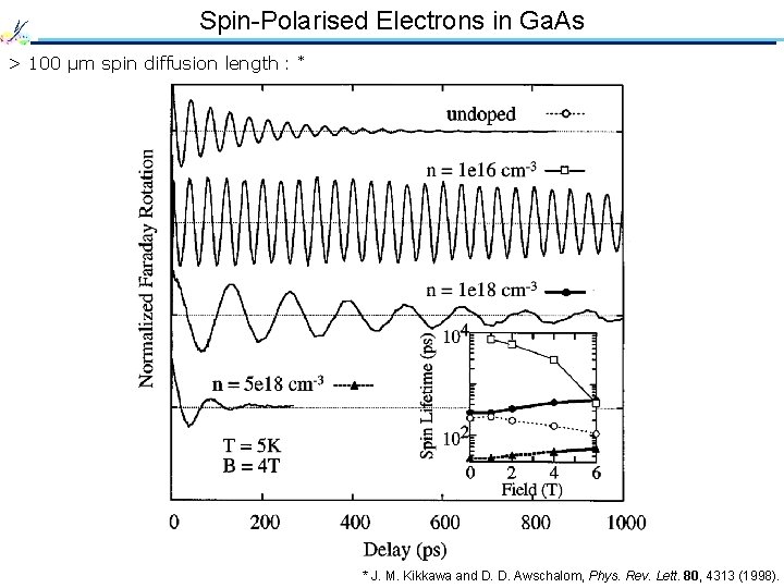
Spin-Polarised Electrons in Ga. As > 100 µm spin diffusion length : * * J. M. Kikkawa and D. D. Awschalom, Phys. Rev. Lett. 80, 4313 (1998).

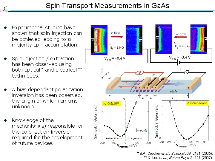
Spin Transport Measurements in Ga. As l Experimental studies have shown that spin injection can be achieved leading to a majority spin accumulation. l Spin injection / extraction has been observed using both optical * and electrical ** techniques. l A bias dependant polarisation inversion has been observed, the origin of which remains unknown. l Knowledge of the mechanism(s) responsible for the polarisation inversion required for the development of future devices. * S. A. Crooker et al. , Science 309, 2191 (2005); ** X. Lou et al. , Nature Phys. 3, 197 (2007).

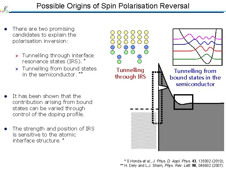
Possible Origins of Spin Polarisation Reversal l There are two promising candidates to explain the polarisation inversion: Tunnelling through interface resonance states (IRS). * Ø Tunnelling from bound states in the semiconductor. ** Ø l It has been shown that the contribution arising from bound states can be varied through control of the doping profile. l The strength and position of IRS is sensitive to the atomic interface structure. * Tunnelling through IRS Tunnelling from bound states in the semiconductor * S Honda et al. , J. Phys. D: Appl. Phys. 43, 135002 (2010); ** H. Dery and L. J. Sham, Phys. Rev. Lett. 98, 046602 (2007).

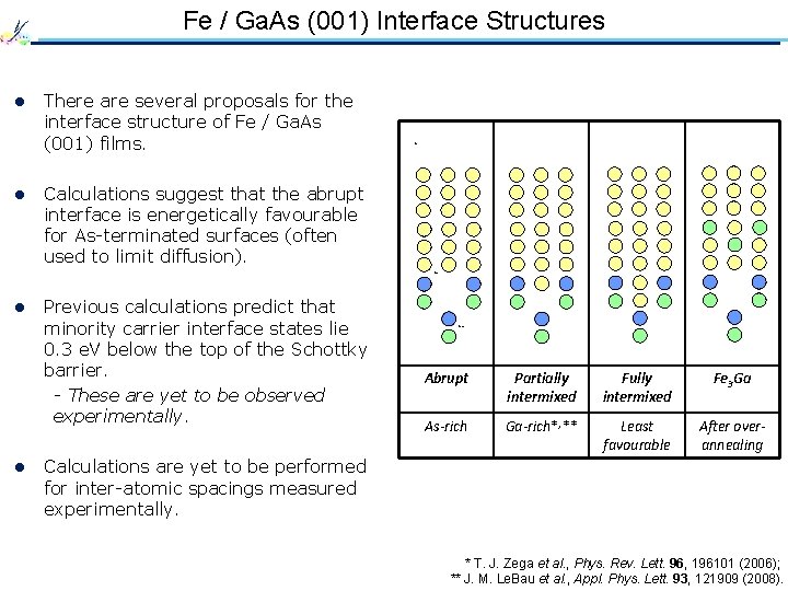
Fe / Ga. As (001) Interface Structures l l There are several proposals for the interface structure of Fe / Ga. As (001) films. Fe Calculations suggest that the abrupt interface is energetically favourable for As-terminated surfaces (often used to limit diffusion). As l l Previous calculations predict that minority carrier interface states lie 0. 3 e. V below the top of the Schottky barrier. - These are yet to be observed experimentally. Ga Abrupt Partially intermixed Fully intermixed Fe 3 Ga As-rich Ga-rich*, ** Least favourable After overannealing Calculations are yet to be performed for inter-atomic spacings measured experimentally. * T. J. Zega et al. , Phys. Rev. Lett. 96, 196101 (2006); ** J. M. Le. Bau et al. , Appl. Phys. Lett. 93, 121909 (2008).

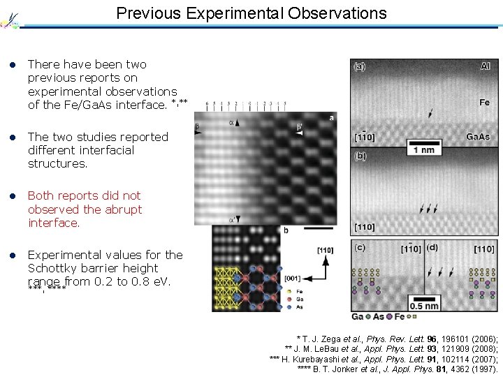
Previous Experimental Observations l There have been two previous reports on experimental observations of the Fe/Ga. As interface. *, ** l The two studies reported different interfacial structures. l Both reports did not observed the abrupt interface. l Experimental values for the Schottky barrier height range from 0. 2 to 0. 8 e. V. ***, **** * T. J. Zega et al. , Phys. Rev. Lett. 96, 196101 (2006); ** J. M. Le. Bau et al. , Appl. Phys. Lett. 93, 121909 (2008); *** H. Kurebayashi et al. , Appl. Phys. Lett. 91, 102114 (2007); **** B. T. Jonker et al. , J. Appl. Phys. 81, 4362 (1997).

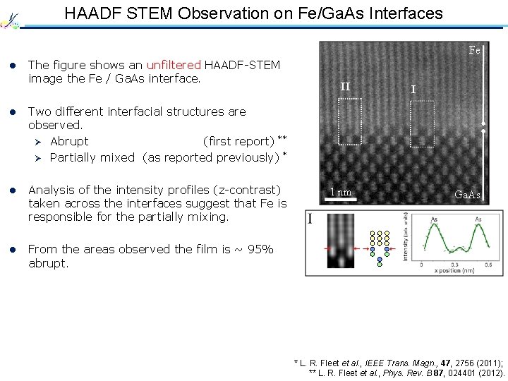
HAADF STEM Observation on Fe/Ga. As Interfaces Fe l The figure shows an unfiltered HAADF-STEM image the Fe / Ga. As interface. l Two different interfacial structures are observed. Ø Abrupt (first report) ** Ø Partially mixed (as reported previously) * l Analysis of the intensity profiles (z-contrast) taken across the interfaces suggest that Fe is responsible for the partially mixing. l From the areas observed the film is ~ 95% abrupt. II 1 nm I Ga. As * L. R. Fleet et al. , IEEE Trans. Magn. , 47, 2756 (2011); ** L. R. Fleet et al. , Phys. Rev. B 87, 024401 (2012).

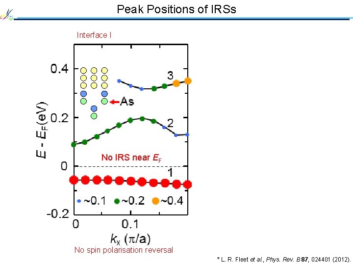
Peak Positions of IRSs Interface I No IRS near EF No spin polarisation reversal Interface II IRS near EF Spin polarisation reversal * L. R. Fleet et al. , Phys. Rev. B 87, 024401 (2012).

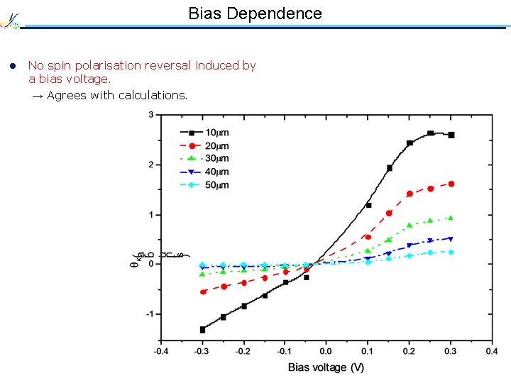
Bias Dependence l No spin polarisation reversal induced by a bias voltage. → Agrees with calculations.

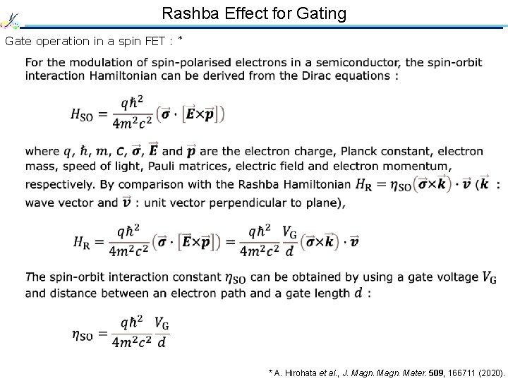
Rashba Effect for Gating Gate operation in a spin FET : * * A. Hirohata et al. , J. Magn. Mater. 509, 166711 (2020).

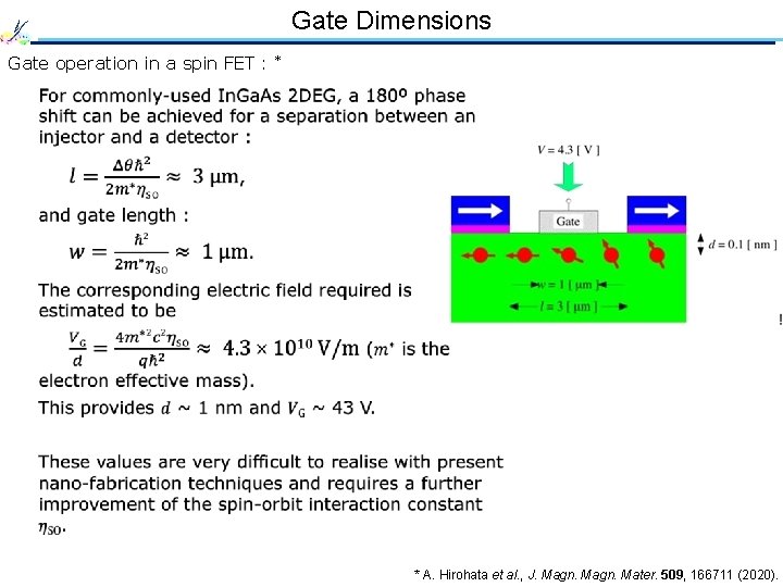
Gate Dimensions Gate operation in a spin FET : * * A. Hirohata et al. , J. Magn. Mater. 509, 166711 (2020).

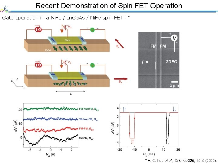
Recent Demonstration of Spin FET Operation Gate operation in a Ni. Fe / In. Ga. As / Ni. Fe spin FET : * * H. C. Koo et al. , Science 325, 1515 (2009).

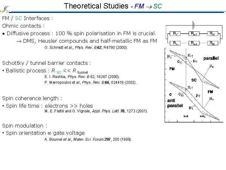
Theoretical Studies - FM SC FM / SC Interfaces : Ohmic contacts : • Diffusive process : 100 % spin polarisation in FM is crucial. DMS, Heusler compounds and half-metallic FM as FM G. Schmidt et al. , Phys. Rev. B 62, R 4790 (2000). Schottky / tunnel barrier contacts : • Ballistic process : R SC << R tunnel E. I. Rashba, Phys. Rev. B 62, 16267 (2000). P. Mavropoulos et al. , Phys. Rev. B 66, 024416 (2002). Spin coherence length : • Spin life time : electrons >> holes M. E. Flatté and G. Vignale, Appl. Phys. Lett. 78, 1273 (2001). Spin modulation : • Spin orientation gate voltage A. Bournel et al. , Mater. Sci. Forum 297, 205 (1999).

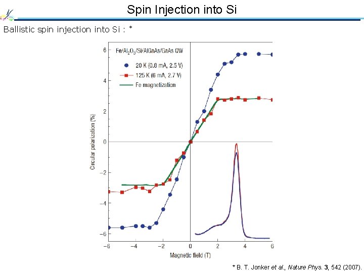
Spin Injection into Si Ballistic spin injection into Si : * * B. T. Jonker et al. , Nature Phys. 3, 542 (2007).

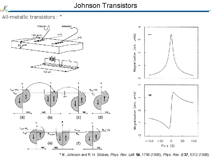
Johnson Transistors All-metallic transistors : * injector detector (50 mm) * M. Johnson and R. H. Silsbee, Phys. Rev. Lett. 56, 1790 (1985), Phys. Rev. B 37, 5312 (1988).

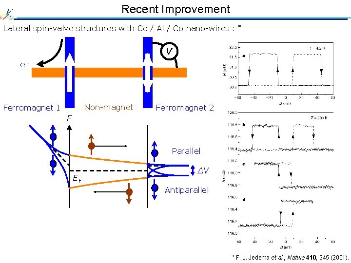
Recent Improvement Lateral spin-valve structures with Co / Al / Co nano-wires : * V e- Non-magnet Ferromagnet 1 Ferromagnet 2 E Parallel EF ∆V Antiparallel * F. J. Jedema et al. , Nature 410, 345 (2001).

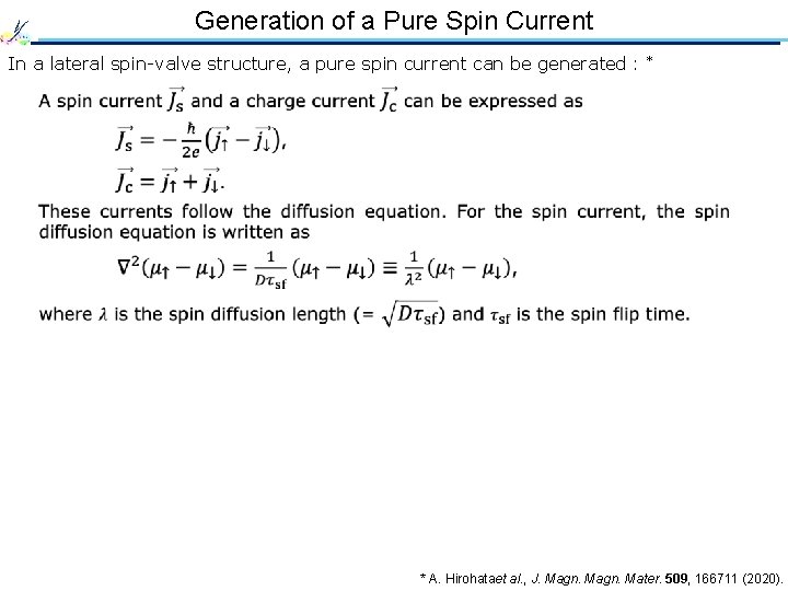
Generation of a Pure Spin Current In a lateral spin-valve structure, a pure spin current can be generated : * * A. Hirohataet al. , J. Magn. Mater. 509, 166711 (2020).

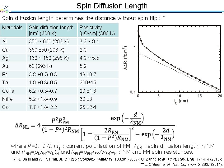
Spin Diffusion Length Spin diffusion length determines the distance without spin flip : Materials Spin diffusion length [nm] (300 K) Resistivity [µΩ·cm] (300 K) Al 350 ~ 600 (293 K) 3. 2 ~ 9. 1 Cu 350 ± 50 (293 K) 2. 9 Ag 132 ~ 152 (298 K) 4. 9 ~ 5. 5 Au 60 (293 K) 5. 2 Pt 3. 8 +0. 7/-0. 3 18 ± 0. 7 Ta 1. 9 +0. 3/-0. 5 200± 15 Co. Fe 6. 2 +0. 3/-0. 7 20 ± 1. 3 Ni. Fe 5. 2 +1. 8/-0. 9 30 ± 3 Co 7. 7 +1. 8/-2. 2 25 ± 2. 4 * where P=I↑−I↓/I↑+I↓ : current polarisation of FM, λNM : spin diffusion length in NM and RNM=ρNλN/w. Nt. N and RFM=ρFMλFM/w. FMw. N : NM and FM spin resistances. • J. Bass and W. P. Pratt, Jr. J. Phys. : Condens. Matter 19, 183201 (2007); G. Zahnd et al. , Phys. Rev. B 98, 174414 (2018); ** L. O’Brien et al. , Nat. Commun. 5, 3927 (2014).