Reducing Crosstalk in Vertically Integrated CMOS Image Sensors







- Slides: 28

Reducing Crosstalk in Vertically. Integrated CMOS Image Sensors Orit Skorka and Dileepan Joseph University of Alberta, Canada

Introduction

Vertically-integrated image sensors � Vertical-integration is a new trend in IC design. � Each die can be fabricated in a process optimized for the devices it contains. � Image sensors contain photodetectors, analog circuits, and digital circuits. � More degrees of freedom in the design of the photodetector; no longer limited to a certain CMOS process. 3

Vertically-integrated image sensors � Vertical stacking allows more circuits to be placed within the same pixel area. � Enables reasonable pixel dimensions while having: � More pixel-level electronics to improve signal -to-noise ratio (SNR) and dynamic range (DR); � High fill-factor. 4

Background

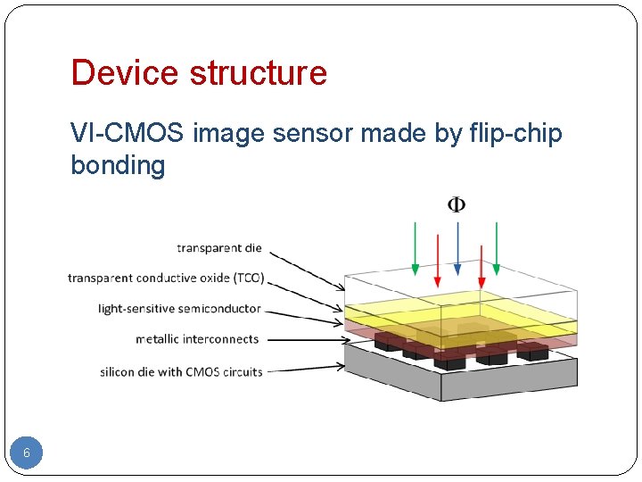
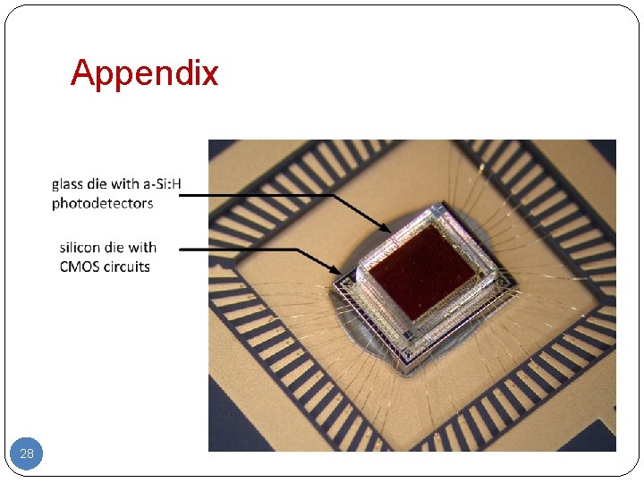
Device structure VI-CMOS image sensor made by flip-chip bonding 6

Reduction of crosstalk � Crosstalk – A situation where signals reach destinations other than their original ones. � Flow of lateral currents in the light- sensitive semiconductor can cause crosstalk in the VI-CMOS image sensor shown. � Lateral currents are caused by drift and diffusion of charge carriers. 7

Reduction of crosstalk � One way to prevent flow of lateral currents is by device patterning. However: � Edges of patterned devices introduce imperfections and defect states; � The additional lithography steps increase the overall manufacturing costs. � In standard CMOS image sensors, the photodetector must have well-defined borders. Therefore, the problem is unique to VI-CMOS image sensors. 8

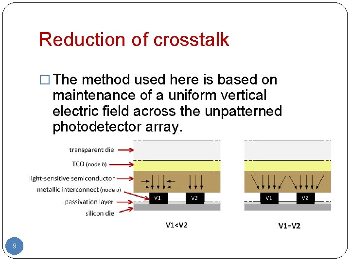
Reduction of crosstalk � The method used here is based on maintenance of a uniform vertical electric field across the unpatterned photodetector array. 9

Primary circuit requirements � Although this idea has been used by Schneider et al. , they do not address important design considerations such as stability and compensation. � In standard CMOS APS image sensors, the read-out is based on the voltage across the photodetector. � Since the photodetector voltage must be kept constant, its current should be used as the input signal. 10 � For an efficient design, one needs to know

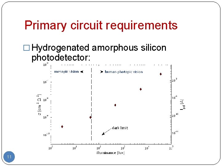
Primary circuit requirements � Hydrogenated amorphous silicon photodetector: 11

Proposed solution � With a proper design of the read-out circuit, a high DR image sensor can be made with a-Si: H photodetectors. � Logarithmic response is preferred because it supports a higher DR than a linear one. � To conclude circuit requirements: � Maintain a constant voltage on the 12 photodetector; � Use Ipd as the input signal; � Have a logarithmic response to

Method

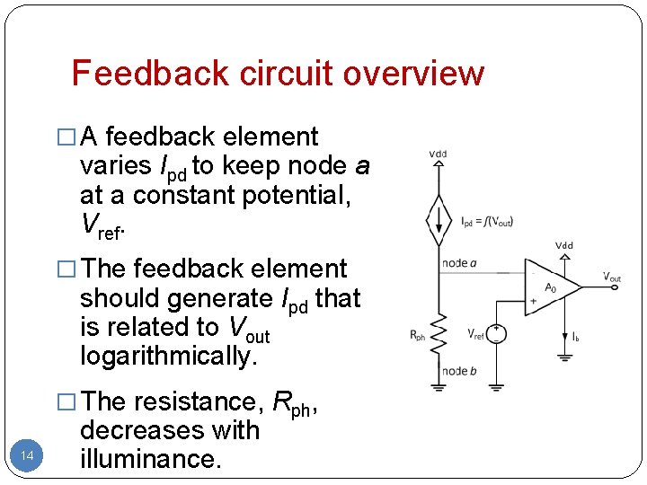
Feedback circuit overview � A feedback element varies Ipd to keep node a at a constant potential, Vref. � The feedback element should generate Ipd that is related to Vout logarithmically. � The resistance, Rph, 14 decreases with illuminance.

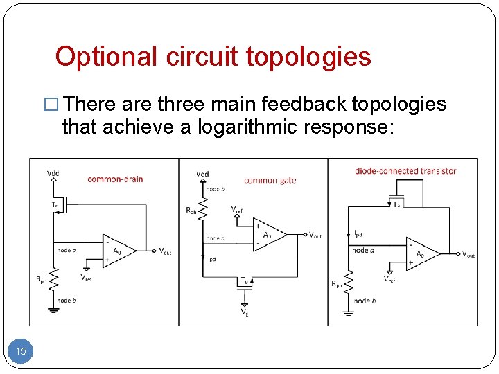
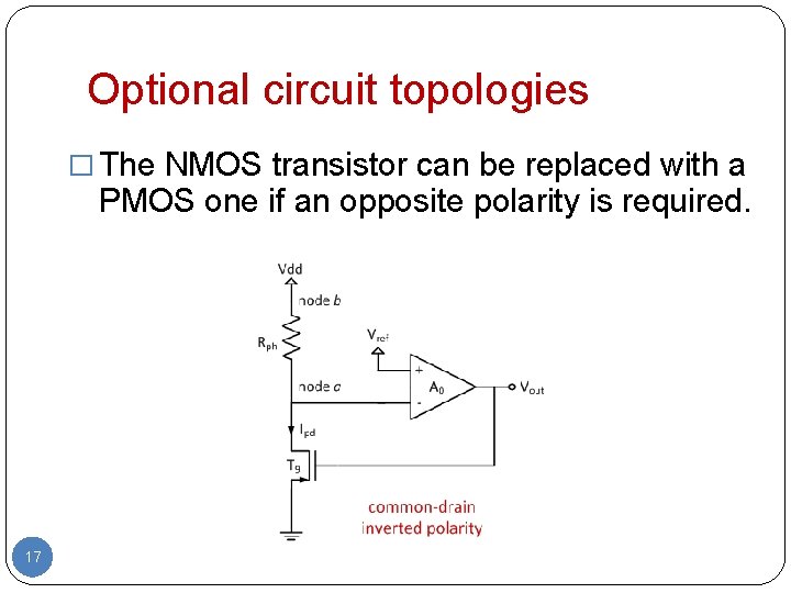
Optional circuit topologies � There are three main feedback topologies that achieve a logarithmic response: 15

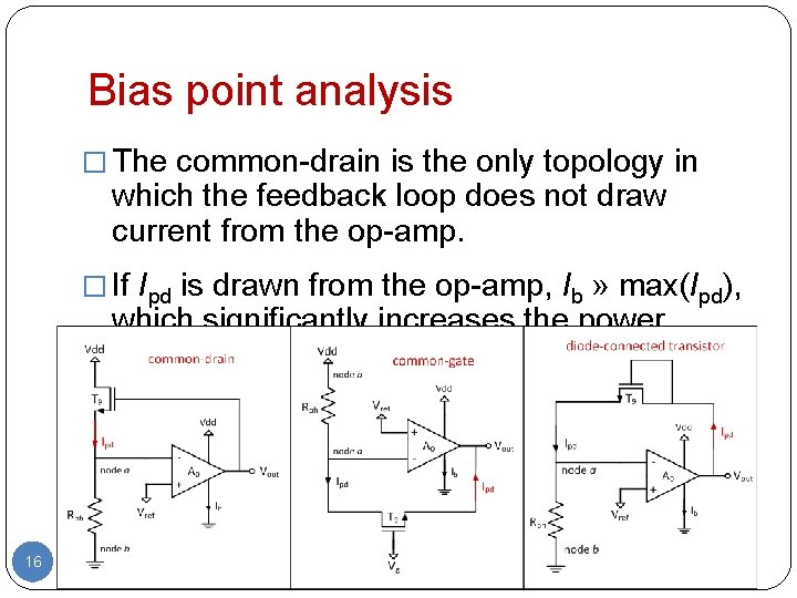
Bias point analysis � The common-drain is the only topology in which the feedback loop does not draw current from the op-amp. � If Ipd is drawn from the op-amp, Ib » max(Ipd), which significantly increases the power consumption. 16

Optional circuit topologies � The NMOS transistor can be replaced with a PMOS one if an opposite polarity is required. 17

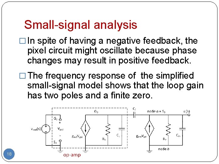
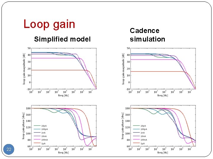
Small-signal analysis � In spite of having a negative feedback, the pixel circuit might oscillate because phase changes may result in positive feedback. � The frequency response of the simplified small-signal model shows that the loop gain has two poles and a finite zero. 18

Results

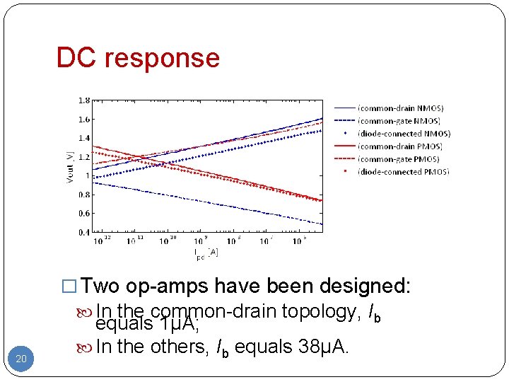
DC response � Two op-amps have been designed: In the common-drain topology, Ib 20 equals 1µA; In the others, Ib equals 38µA.

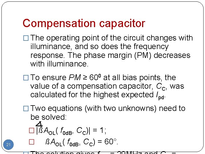
Compensation capacitor � The operating point of the circuit changes with illuminance, and so does the frequency response. The phase margin (PM) decreases with illuminance. � To ensure PM ≥ 600 at all bias points, the value of a compensation capacitor, CC, was calculated for the highest expected Ipd. � Two equations (with two unknowns) need to be solved: � |ßAOL( f 0 d. B, CC)| = 1; 21 � ßAOL( f 0 d. B, CC) = 60°.

Loop gain Simplified model 22 Cadence simulation

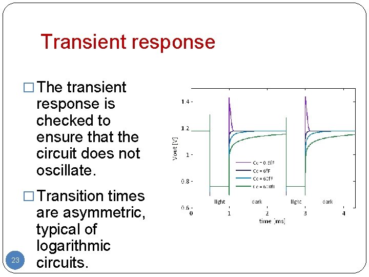
Transient response � The transient response is checked to ensure that the circuit does not oscillate. � Transition times 23 are asymmetric, typical of logarithmic circuits.

Conclusion

Conclusion � This work introduced circuits to reduce crosstalk in VI-CMOS image sensors with an unpatterned photodetector array. � Flow of lateral currents can be reduced by applying a constant electric potential at all pixels of the unpatterned photodetector array. � The read-out circuit is required to: � Maintain a constant potential at the 25 photodetector; � Use the photodetector current as the input signal;

Conclusion � The circuit is implemented using a logarithmic amplifier with feedback control. � The common-drain configuration is found to be the most power efficient. � A simplified small-signal model of the circuit has been developed to test the system for stability and determine the value of the compensation capacitor. � Transient simulations confirm that the 26 circuit does not oscillate in bright light when CC is added.

Acknowledgments The authors gratefully acknowledge the support of: � Alberta Ingenuity; � The Natural Sciences and Engineering Research Council (NSERC) of Canada; � Micralyne Inc; � CMC Microsystems. 27

Appendix 28