Nano technology John Summerscales School of Engineering University



- Slides: 30

Nano technology John Summerscales School of Engineering University of Plymouth

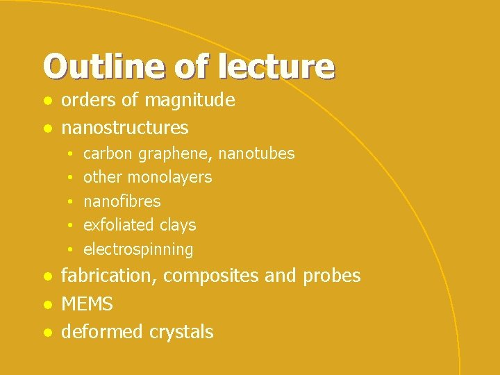
Outline of lecture l l orders of magnitude nanostructures • • • l l l carbon graphene, nanotubes other monolayers nanofibres exfoliated clays electrospinning fabrication, composites and probes MEMS deformed crystals

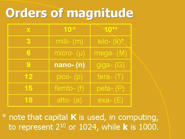
Orders of magnitude x 10 -x 10+x 3 milli- (m) kilo- (k)* 6 micro- (μ) mega- (M) 9 nano- (n) giga- (G) 12 pico- (p) tera- (T) 15 femto- (f) peta- (P) 18 atto- (a) exa- (E) * note that capital K is used, in computing, to represent 210 or 1024, while k is 1000.

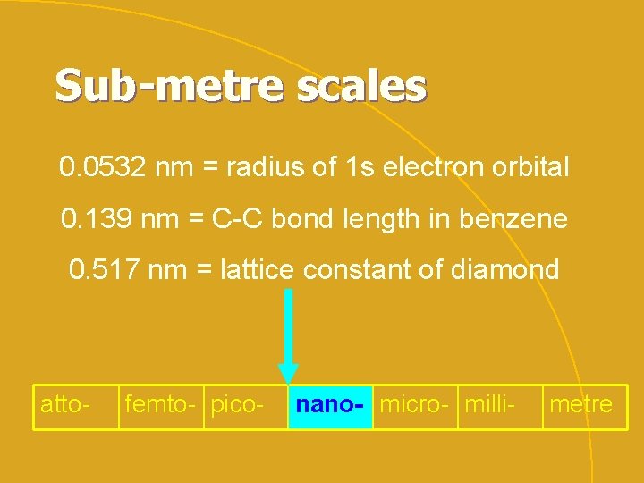
Sub-metre scales 0. 0532 nm = radius of 1 s electron orbital 0. 139 nm = C-C bond length in benzene 0. 517 nm = lattice constant of diamond atto- femto- pico- nano- micro- milli- metre

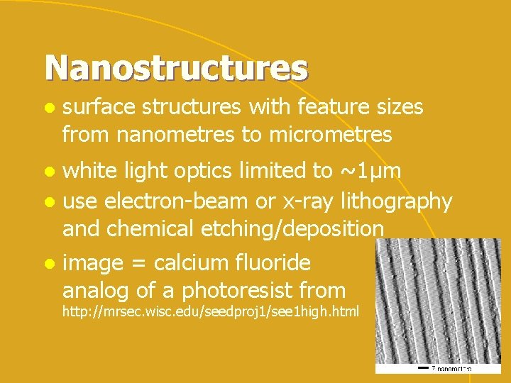
Nanostructures l surface structures with feature sizes from nanometres to micrometres white light optics limited to ~1μm l use electron-beam or x-ray lithography and chemical etching/deposition l l image = calcium fluoride analog of a photoresist from http: //mrsec. wisc. edu/seedproj 1/see 1 high. html

Carbon Elemental carbon may be • amorphous or one of two crystalline forms: • diamond (cubic crystal sp 3 structure) • graphite (contiguous sp 2 sheets) • graphene (single atom thickness layers of graphite) or at nanoscale can combine to form • spheres (buckminsterfullerenes or “bucky balls”) • and/or nanotubes or other allotropes, including • graph(a/o/y/idy)ne and novamene (sp 3/sp 2)

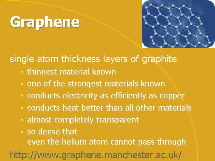
Graphene single atom thickness layers of graphite • • • thinnest material known one of the strongest materials known conducts electricity as efficiently as copper conducts heat better than all other materials almost completely transparent so dense that even the helium atom cannot pass through http: //www. graphene. manchester. ac. uk/

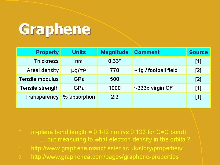
Graphene Property Units Magnitude Thickness nm 0. 33* μg/m 2 770 Tensile modulus GPa 500 Tensile strength GPa 1000 Areal density Transparency % absorption * 1. 2. Comment Source [1] ~1 g / football field [2] ~333 x virgin CF 2. 3 in-plane bond length = 0. 142 nm (vs 0. 133 for C=C bond). . . but measuring to what electron density in the orbital? http: //www. graphene. manchester. ac. uk/story/properties/ http: //www. graphenea. com/pages/graphene-properties [1]

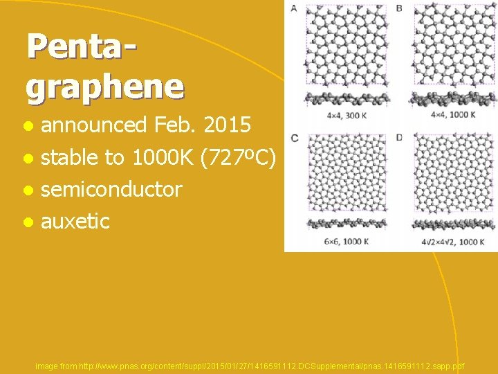
Pentagraphene announced Feb. 2015 l stable to 1000 K (727ºC) l semiconductor l auxetic l image from http: //www. pnas. org/content/suppl/2015/01/27/1416591112. DCSupplemental/pnas. 1416591112. sapp. pdf

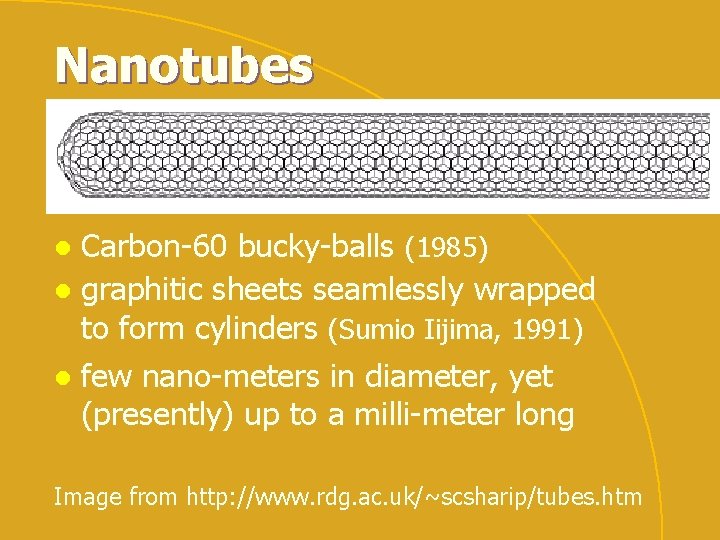
Nanotubes Carbon-60 bucky-balls (1985) l graphitic sheets seamlessly wrapped to form cylinders (Sumio Iijima, 1991) l l few nano-meters in diameter, yet (presently) up to a milli-meter long Image from http: //www. rdg. ac. uk/~scsharip/tubes. htm

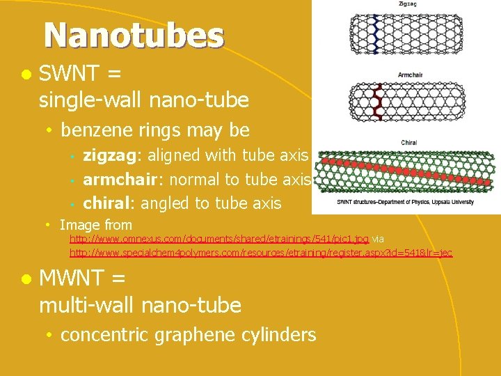
Nanotubes l SWNT = single-wall nano-tube • benzene rings may be • • • zigzag: aligned with tube axis armchair: normal to tube axis chiral: angled to tube axis • Image from http: //www. omnexus. com/documents/shared/etrainings/541/pic 1. jpg via http: //www. specialchem 4 polymers. com/resources/etraining/register. aspx? id=541&lr=jec l MWNT = multi-wall nano-tube • concentric graphene cylinders

Nanotube production arc discharge through high purity graphite electrodes in low pressure helium (He) l laser vapourisation of a graphite target sealed in argon (Ar) at 1200°C. l electrolysis of graphite electrodes immersed in molten lithium chloride under an Ar. l CVD of hydrocarbons in the presence of metals catalysts. l concentrating solar energy onto carbon-metal target in an inert atmosphere. l

Nanotube purification oxidation at 700°C (<5% yield) l filtering colloidal suspensions l ultrasonically assisted microfiltration l microwave heating together with acid treatments to remove residual metals. l

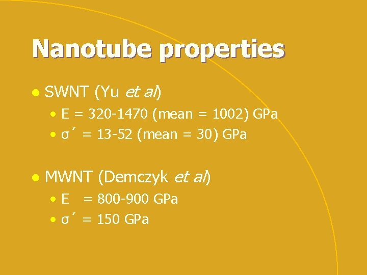
Nanotube properties l SWNT (Yu et al) • E = 320 -1470 (mean = 1002) GPa • σ´ = 13 -52 (mean = 30) GPa l MWNT (Demczyk et al) • E = 800 -900 GPa • σ´ = 150 GPa

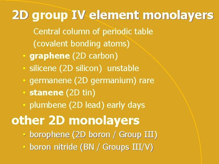
2 D group IV element monolayers • • • Central column of periodic table (covalent bonding atoms) graphene (2 D carbon) silicene (2 D silicon) unstable germanene (2 D germanium) rare stanene (2 D tin) plumbene (2 D lead) early days other 2 D monolayers • borophene (2 D boron / Group III) • boron nitride (BN / Groups III/V)

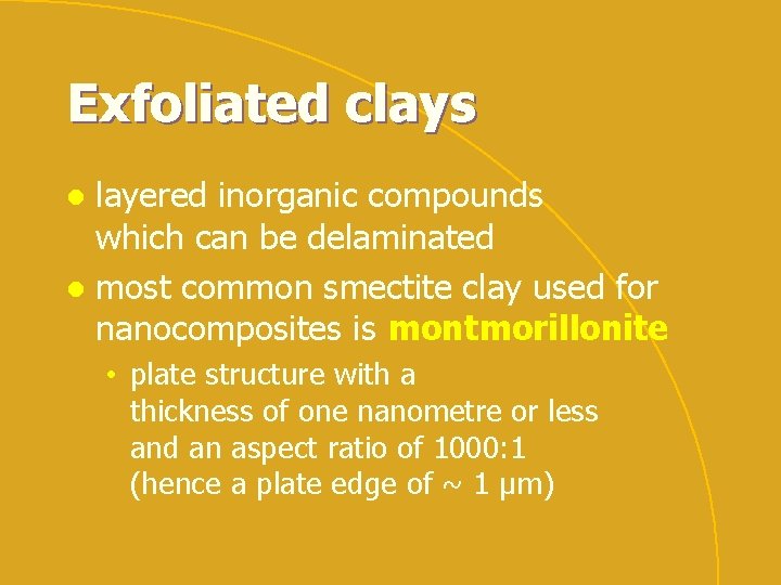
Exfoliated clays layered inorganic compounds which can be delaminated l most common smectite clay used for nanocomposites is montmorillonite l • plate structure with a thickness of one nanometre or less and an aspect ratio of 1000: 1 (hence a plate edge of ~ 1 μm)

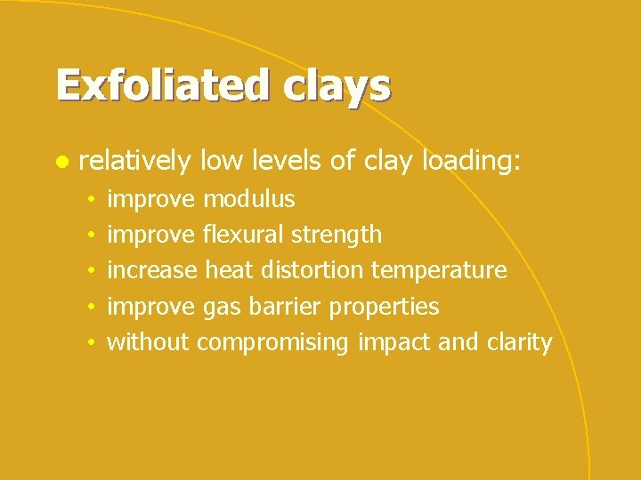
Exfoliated clays l relatively low levels of clay loading: • • • improve modulus improve flexural strength increase heat distortion temperature improve gas barrier properties without compromising impact and clarity

Nano-fabrication l electrospinning chemical vapour deposition electron beam or UV lithography pulsed laser deposition l composites l l l • nano-particle agglomeration (clustering)

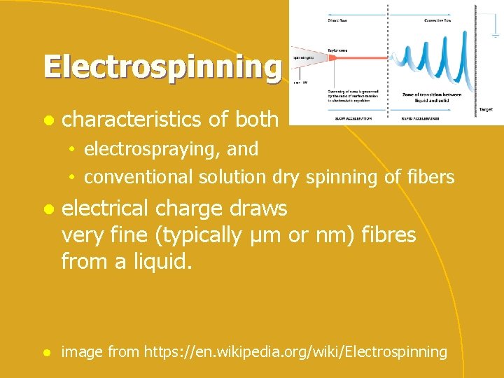
Electrospinning l characteristics of both • electrospraying, and • conventional solution dry spinning of fibers l l electrical charge draws very fine (typically μm or nm) fibres from a liquid. image from https: //en. wikipedia. org/wiki/Electrospinning

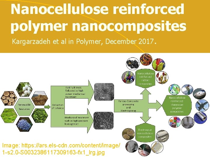
Nanocellulose reinforced polymer nanocomposites Kargarzadeh et al in Polymer, December 2017. Image: https: //ars. els-cdn. com/content/image/ 1 -s 2. 0 -S 0032386117309163 -fx 1_lrg. jpg

Curran®: carrot fibres l Cellu. Comp (Scotland) • nano-fibres extracted from vegetables • carrot nano-fibres claimed to have: • • • modulus of 130 GPa strengths up to 5 GPa failure strains of over 5% • potential for turnips, swede and parsnips • 1 st product: "Just Cast“ composite fly-fishing rod.

Nano-probes l l l atomic force microscope scanning tunnelling microscope superconducting quantum interference device (SQUID)

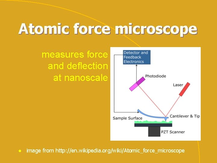
Atomic force microscope measures force and deflection at nanoscale l image from http: //en. wikipedia. org/wiki/Atomic_force_microscope

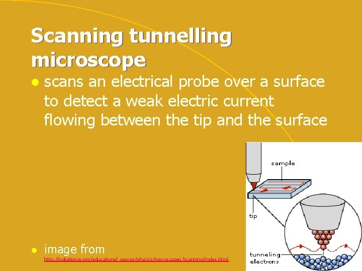
Scanning tunnelling microscope l l scans an electrical probe over a surface to detect a weak electric current flowing between the tip and the surface image from http: //nobelprize. org/educational_games/physics/microscopes/scanning/index. html

Superconducting QUantum Interference Device (SQUID) measures extremely weak magnetic signals l e. g. subtle changes in the electromagnetic energy field of the human body. l

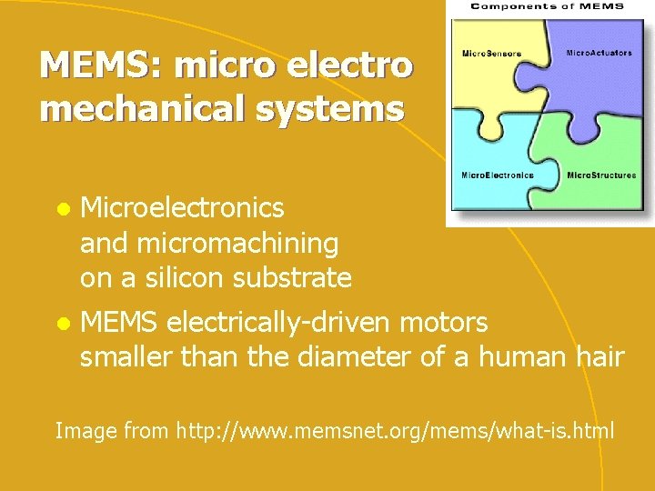
MEMS: micro electro mechanical systems l Microelectronics and micromachining on a silicon substrate l MEMS electrically-driven motors smaller than the diameter of a human hair Image from http: //www. memsnet. org/mems/what-is. html

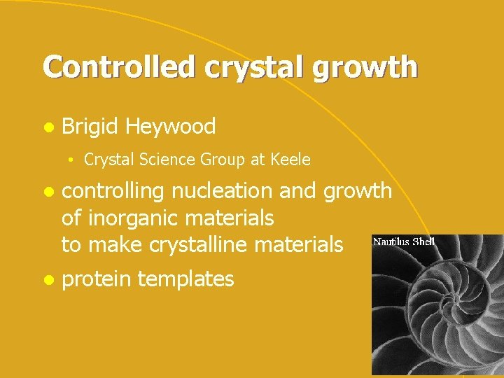
Controlled crystal growth l Brigid Heywood • Crystal Science Group at Keele l controlling nucleation and growth of inorganic materials to make crystalline materials l protein templates

Summary l l orders of magnitude nanostructures • • • l l l carbon graphene, nanotubes other monolayers nanofibres exfoliated clays electrospinning fabrication, composites and probes MEMS deformed crystals

Acknowledgements l Various websites from which images have been extracted

To contact me: J Dr John Summerscales * ACMC/SMSE, Reynolds Room 008 ) 2 < University of Plymouth Devon PL 4 8 AA 01752. 5. 86150 01752. 5. 86101 jsummerscales@plymouth. ac. uk : http: //www. plymouth. ac. uk/staff/jsummerscales