Nano Materials and Nano Technology Concepts of Nanoscience
- Slides: 31

Nano Materials and Nano. Technology

Concepts of Nanoscience & Nanotechnology - direct control of materials and devices on molecular and atomic scale includes fabrication of nano structures, synthesis and process of nano particles, etc.

Nano Levels are occurring in a verity of fields and requires knowledge Physics – behavior of matter below a certain scale and interaction of atoms Chemistry –interaction of different materials with each other at designing part Biology – how biological system works at lowest level Computer Science – exchange the information and collection of large amount of data Electrical Engineering – generate and manage power more efficiently Mechanical Engineering – issues to be seen like load bearing, material fatigue and

Nano Materials Made up of grains Diameter of grains are about 100 nm Contains less than few ten thousand atoms One nano meter = one billionth of a meter

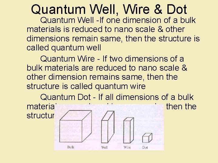
Quantum Well, Wire & Dot Quantum Well -If one dimension of a bulk materials is reduced to nano scale & other dimensions remain same, then the structure is called quantum well Quantum Wire - If two dimensions of a bulk materials are reduced to nano scale & other dimension remains same, then the structure is called quantum wire Quantum Dot - If all dimensions of a bulk materials are reduced to nano scale, then the structure is called quantum dot

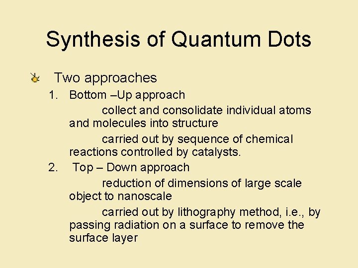
Synthesis of Quantum Dots Two approaches 1. Bottom –Up approach collect and consolidate individual atoms and molecules into structure carried out by sequence of chemical reactions controlled by catalysts. 2. Top – Down approach reduction of dimensions of large scale object to nanoscale carried out by lithography method, i. e. , by passing radiation on a surface to remove the surface layer

Unique Properties of Nanomaterials Very high magneto resistance Low melting point High solid state phase transition pressure High self diffusion coefficient High catalytic activity Lower ferro eclectric transition temperature

Variation of Physical Properties Electron affinities and chemical properties with Size - electronic bonds become narrower size - delocalized electron states become localized - ionization potential and reactivity are higher at smaller - strong catalyst effect Magnetic Properties - exhibit totally new class of magnetic properties - ferro and anti ferro magnets exhibit giant magneto resistance - low coordination number Mechanical behavior - low melting point - high strength because its free from dislocation - super hardness

Technological Advantages Improved Transportation Inexpensive shatter proof diamond is used to make air planes. Unloaded weight is fifty times lighter than aluminum but strong. capacity can be increased Atom Computers Designing gates with less than 1000 atoms, which have to be in right place can be build mass storage device and store hundred billion bytes in a size of sugar cube can deliver a billion of instructions per second Military Applications Smart weapons can be made the size of a bullet rapid , inexpensive, stronger can be made and can be guided by the computer which is more power than super computer Navigation, tracking can be done by this computer Solar Energy inexpensive and efficient can be made Medical Uses heeling the injuries at the molecular and cellular level that are causes of disease

Carbon Nanotubes - thin and long straw shaped, that is tubular forms Carbon - graphene sheets rolled into cylindrical form - diameter is few nanometers & length is several micrometers - made up of hexagonal covalent bonded carbon atoms Two types Single Walled Carbon Nanotubes (SWNT) consists of single graphene cylinder Multi Walled Carbon Nanotubes (MWNT) consists of several graphene cylinders

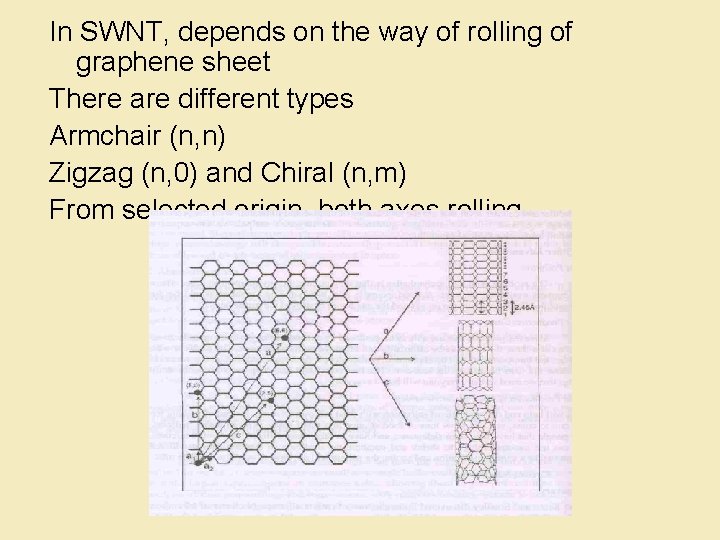
In SWNT, depends on the way of rolling of graphene sheet There are different types Armchair (n, n) Zigzag (n, 0) and Chiral (n, m) From selected origin, both axes rolling

Properties of Carbon Chemical Reactivity Nanotubes - related to an increased curvature - distinction should be made between side walls and end caps - smaller diameter increases reactivity - solubility can be controlled Electrical Conductivity - depends on chiral vector, it will be either semiconductor or metal - conducting properties derived from graphene sheet properties - if n=m, metal - resistance independent of length Optical Activity - disappears when NT length becomes longer Mechanical Strength - very large Young Modulus in axial direction - very flexible because of its great length - suitable for composite material

Unique Properties High electrical conductivity Very high tensile strength High flexible, very elastic High thermal conductivity but low thermal expansion coefficient Highly absorbent

Synthesis of Carbon Three commonly used methods Nanotubes Laser ablation Intense laser pulses fall on the graphite and it gets blasted. Plasma plume is generated from which SWNTs form Arc discharge method When power supply is applied to two graphite rods which are placed few millimeters apart, carbon vaporizes and nanotubes forms Chemical vapor deposition Place gaseous carbon in energy source such as plasma or heated coil. The energy source is used to crack the molecule into a reactive radical species and diffuse down to substrate, which is heated then carbon nanotubes form

Applications of CNTs Energy Storage a) Hydrogen Storage hydrogen liquid or gas can be stored in the inner core through capillary effect and hydrogen atom is absorbed, is called chemisorption b) Lithium intercalation all interstitial sites such as inter shells, inter tube channels and inner cores are accessible for Li intercalation. It is reversible and irreversible. In nanotubes is still unsuitable for batteries but in future it suits by altering the nanotubes c) Electrochemical Super capacitors capacity of energy depends the separation between the electrode and charge in electrolyte. If nanotubes are used as electrolyte and electrodes. Very large energy can be stored by small applied

Molecular electronics with Field Emitting Devices CNT extract an electron from the solid surface potential barrier by high applied electric field. an ideal emitter requires nano meter diameter, low threshold emission field, high electrical conductivity, chemical stability. CNT possess all the properties. Used in electron microscopes, telecom network Transistors by applying voltage to a gate electrode ie. CNT, it can be switch from conducting state to insulating state, that is, it works as a switch Nanoprobes and Sensors as a scanning probe, in STM and AFM. It does get suffered from crashes because of high elasticity. Used as molecular probes because modified by chemically Composites used as reinforcements because of its stiffness, high strength, low weight, high flexible. used in polymer composites, it will increase toughness by absorbing energy during the elastic behavior used as membrane for molecular separation Templates holding gas and fluids

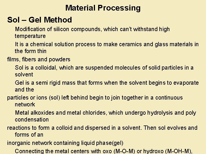
Material Processing Sol – Gel Method Modification of silicon compounds, which can’t withstand high temperature It is a chemical solution process to make ceramics and glass materials in the form thin films, fibers and powders Sol is a colloidal, which are suspended molecules of solid particles in a solvent Gel is a semi rigid mass that forms when the solvent begins to evaporate and the particles or ions (sol) left behind begin to join together in a continuous network Metal alkoxides and metal chlorides, which undergo hydrolysis and poly condensation reactions to form a colloid and dispersed in a solvent. Then sol evolves and forms of an inorganic network containing liquid phase(gel) Connecting the metal centers with oxo (M-O-M) or hydroxo (M-OH-M),

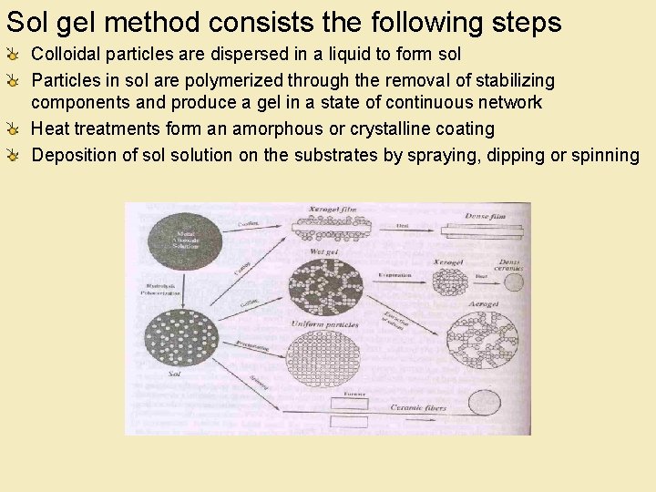
Sol gel method consists the following steps Colloidal particles are dispersed in a liquid to form sol Particles in sol are polymerized through the removal of stabilizing components and produce a gel in a state of continuous network Heat treatments form an amorphous or crystalline coating Deposition of solution on the substrates by spraying, dipping or spinning

Advantage thin coating provides adhesion between the metallic substrate and the top and thick coating provides corrosion protection can shape the materials in gel state and produce the high purity products low temperature sintering, simple, economic and effective method to produce high quality coatings Application used in ceramics production and diverse applications in optics, electronics, energy, sensors, medicine and separation technology used for silicated gel formation

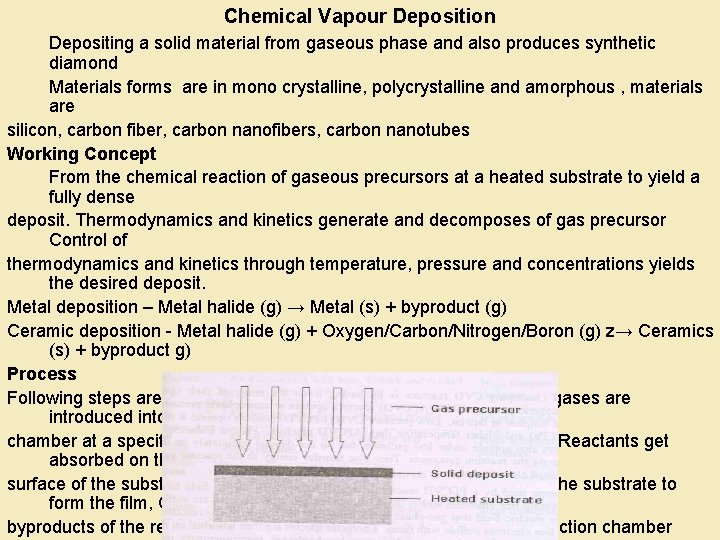
Chemical Vapour Deposition Depositing a solid material from gaseous phase and also produces synthetic diamond Materials forms are in mono crystalline, polycrystalline and amorphous , materials are silicon, carbon fiber, carbon nanofibers, carbon nanotubes Working Concept From the chemical reaction of gaseous precursors at a heated substrate to yield a fully dense deposit. Thermodynamics and kinetics generate and decomposes of gas precursor Control of thermodynamics and kinetics through temperature, pressure and concentrations yields the desired deposit. Metal deposition – Metal halide (g) → Metal (s) + byproduct (g) Ceramic deposition - Metal halide (g) + Oxygen/Carbon/Nitrogen/Boron (g) z→ Ceramics (s) + byproduct g) Process Following steps are involved, Mix of reactant gases and diluent inert gases are introduced into the reaction chamber at a specified flow rate, Gas species move to the substrate, Reactants get absorbed on the surface of the substrate, Reactants undergo chemical reactions with the substrate to form the film, Gaseous byproducts of the reactions are absorbed and evacuated from the reaction chamber

System consists of Sources and feed lines for gases Mass flow controllers for gases Reaction chamber System for heating During the process, the reactant gas react with Substrate, is known as heterogeneous reaction and occurs on the heated surface. Also the reactant gas react with gas phase in reactor’s atmosphere, is known as homogeneous reaction and produce poor and low density film with lots of defects Types of Chemical vapour deposition Process differs in means of chemical reactions and process condition Two types of reactor wall can be used, one is hot wall, in which the both substrate and the reactor wall are heated another is cold wall, in which only the substrate is heated Based on their operating pressure it is classified. Atmospheric pressure CVD (APCVD), in which the reactors operate at atmospheric pressure and it is simplest in

Advantages & Applications Advantages Used for wide range of metals & ceramics, fabricating complex shapes, high purity deposits, homogeneously joining substrate surface, thickness can be controlled, can be coated powders, multiple components, internal passages Applications used to promote or prevent adhesion, photo resist adhesion in semiconductor, reduce stiction, drift Promote biocompatibility between natural and synthetic materials, anti corrosive coating

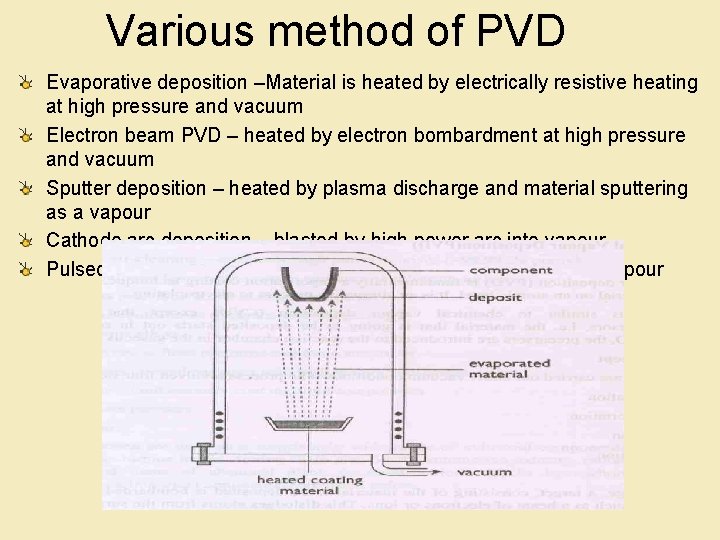
Physical Vapour Deposition It is an alternative process of electroplating, which involves transfer of material on an atomic level. It is similar to CVD except the precursors, that is solid is deposited in PVD Working Concept carried out under vacuum condition, the process involves Evaporation – Material (target) to be deposited is bombarded by a high energy such as beam of electrons or ions, to vaporize the atoms Transport – Movement of vaporized atoms from the material (target) to the substrate Reaction – In case of target material with metal, the atoms of metal will react with appropriate gas during the transport stage and for target material alone then this process would not be part of the process Deposition – process of coating on the substrate. Reaction between target materials and reactive gases may take place at the substrate with the deposition process Target material is placed in a vacuum champer, due to intense heat the target material is evaporated then the coating is formed

Various method of PVD Evaporative deposition –Material is heated by electrically resistive heating at high pressure and vacuum Electron beam PVD – heated by electron bombardment at high pressure and vacuum Sputter deposition – heated by plasma discharge and material sputtering as a vapour Cathode arc deposition – blasted by high power arc into vapour Pulsed Laser deposition – high power laser is used to produce vapour

Importance To improve hardness, reduce friction and oxidation resistance Advantages Improve the properties of the substrate, inorganic material can be used as organic material and environmental friendly Disadvantages High capital cost, requires skilled operators, large amount of heat and the rate of coating is slow Applications In aerospace, automotive, surgical, dies and moulds, cutting tools and fire arms

Microwave synthesis of Microwaves are form. Materials of electromagnetic energy with the wavelength between 1 mm and 1 m. When the bulk material is placed in the microwave field, material either absorbs, reflects or transparent, which depends on its chemical composition, physical size, shape and frequency of the microwaves. Two principle mechanisms for interaction with matter are 1. Dipole interaction and 2. Ionic conduction. These mechanisms require coupling between material and electric field Dipole interaction occurs with polar molecules. Heat will be produced by friction and moving molecules in the field of microwave. Ionic conduction – Ions don’t have dipole moment , they are distributed and can couple with oscillating electric field of microwaves, produce heat. Heat is a

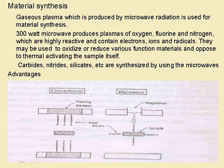
Material synthesis Gaseous plasma which is produced by microwave radiation is used for material synthesis. 300 watt microwave produces plasmas of oxygen, fluorine and nitrogen, which are highly reactive and contain electrons, ions and radicals. They may be used to oxidize or reduce various function materials and oppose to thermal activating the sample itself. Carbides, nitrides, silicates, etc are synthesized by using the microwaves Advantages Greater flexibility, speed, energy savings, product quality, cleaner and more economical. Other heating methods cannot be produced new materials.

Electron Microscopy It is scientific instruments that use a beam of highly energetic Techniques electrons to examine objects on a very fine scale. Electrons wavelength is about. 005 nm, which increase the resolving power. It is used to examine the following information Topography – Surface of an object, which are its texture, hardness, reflectivity, etc. Morphology – Shape and size of the particles making up object and ductility, strength, reactivity, etc. Composition – Elements and compounds that the object is composed and melting point, reactivity, hardness, etc. Crystallographic Information – Arrangement of atoms in the

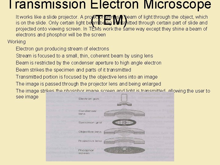
Transmission Electron Microscope (TEM) It works like a slide projector. A projector shines a beam of light through the object, which is on the slide. Only certain light beam being transmitted through certain part of slide and projected onto viewing screen. In TEMs work the same way except they shine a beam of electrons and phosphor will be the screen Working Electron gun producing stream of electrons Stream is focused to a small, thin, coherent beam by using lens Beam is restricted by the condenser aperture to high angle electron Beam strikes the specimen and parts of it transmitted Transmitted portion is focused by the objective lens into an image The image is passed through the projector lens and being enlarged The image strikes the phosphor image screen and light is transmitted, allowing the user to see image

Specimen interactions and Unscattered Electrons utilization Source – Incident electron transmitted without any interaction occurring inside the specimen Utilization – Unscattered electron is inversely proportional to the specimen thickness. Elasticity Scattered electrons Source – Incident electrons that are scattered by atoms in an elastic fashion Utilization – Electrons wavelength =2 X atomic space X angle of scattering and enters normal to surface. Entered electrons scattered by atomic spacing and angle, which are formed a pattern by magnetic lenses. This pattern gives the information about orientation, atomic arrangements and phase present Inelastically Scattered Electrons Source – Incident electron interacts with specimen in a inelastic fashion and losses energy. Then the electrons are transmitted to rest of the specimen Utilization – Electron Energy Loss Spectroscopy – Inelastic loss of energy is characteristic of the elements that were interacted with

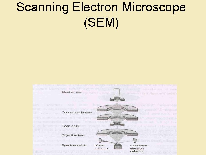
Scanning Electron Microscope (SEM)