Microprocessors 80868088 Hardware Specifications Chapter 8 ACOE 255



- Slides: 16

Microprocessors 8086/8088 Hardware Specifications (Chapter 8) ACOE 255 1

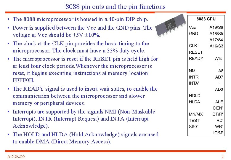
8088 pin outs and the pin functions • The 8088 microprocessor is housed in a 40 -pin DIP chip. • Power is supplied between the Vcc and the GND pins. The voltage at Vcc should be +5 V ± 10%. • The clock at the CLK pin provides the basic timing to the microprocessor. The clock must have a 33% duty cycle. • The microprocessor is reset if the RESET pin is held high for at least four clock periods. Whenever the microprocessor is reset, it begins executing instructions at memory location FFFF 0 H. • The READY signal is used to insert wait states, to enable the communication between the microprocessor and slower memory or peripheral devices. • Interrupts are supported by the signals NMI (Non-Maskable Interrupt), INTR (Interrupt Request) and INTA (Interrupt Acknowledge). • The HOLD and HLDA (Hold Acknowledge) signals are used to enable DMA (Direct Memory Access). ACOE 255 2

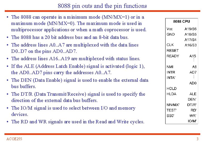
8088 pin outs and the pin functions • The 8088 can operate in a minimum mode (MN/MX=1) or in a maximum mode (MN/MX=0). The maximum mode is used in multiprocessor applications or when a math coprocessor is used. • The 8088 has a 20 bit address bus and an 8 -bit data bus. • The address lines A 0. . A 7 are multiplexed with the data lines D 0. . D 7 on the pins AD 0. . AD 7. • The address lines A 16. . A 19 are multiplexed with status lines. • If the ALE (Address Latch Enable) signal is activated (logic 1), the AD 0. . AD 7 pins carry the addresses A 0. . A 7. • The DEN (Data Enable) signal is used to enable the external data bus buffers. • The DT/R (Data Transmit/Receive) signal is used to specify the direction of the external data bus buffers. • The IO/M signal is used to select between I/O and memory devices. • The RD and WR signals are used in the Read and Write cycles. ACOE 255 3

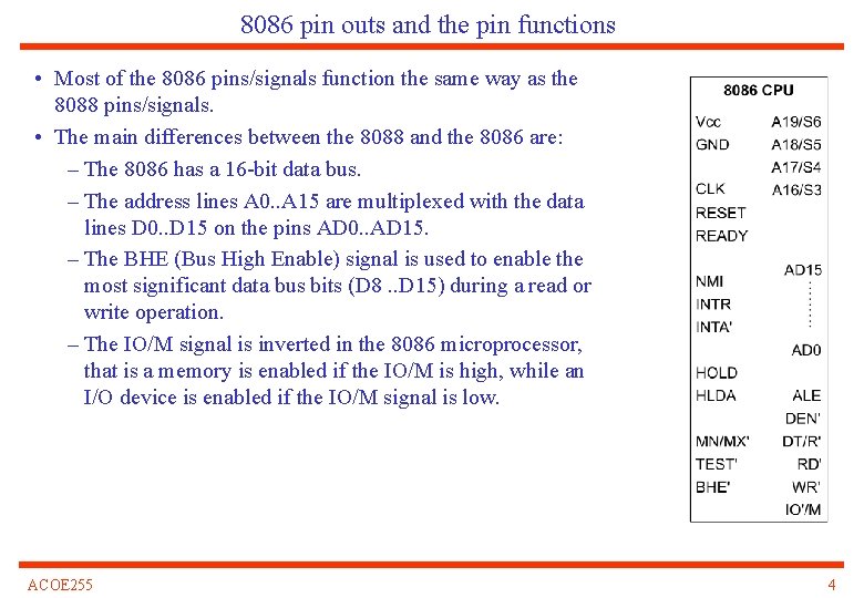
8086 pin outs and the pin functions • Most of the 8086 pins/signals function the same way as the 8088 pins/signals. • The main differences between the 8088 and the 8086 are: – The 8086 has a 16 -bit data bus. – The address lines A 0. . A 15 are multiplexed with the data lines D 0. . D 15 on the pins AD 0. . AD 15. – The BHE (Bus High Enable) signal is used to enable the most significant data bus bits (D 8. . D 15) during a read or write operation. – The IO/M signal is inverted in the 8086 microprocessor, that is a memory is enabled if the IO/M is high, while an I/O device is enabled if the IO/M signal is low. ACOE 255 4

Clock/Reset/Ready Circuit • The 8284 chips serves three purposes: – Generates the main clock (CLK) for the processor (fc/3 with 33% duty cycle) and the clock for the peripheral devices (fc/5). – Provides the Reset pulse according to the state of the RC circuit connected at the RES input. – Provides the Ready signal to insert wait states whenever the processor is accessing slow memory or peripheral I/O ports. ACOE 255 5

Operation of the Reset Circuit • Initially the capacitor is uncharged. When power is switched on, the Reset signal is at logic 1. The capacitor starts charging with time constant (10 K*10 u. F). When the voltage across the capacitor becomes equal to the minimum High voltage of the 8284 (2 V), the Reset signal goes to logic 0. • If the Reset button is pressed, the capacitor is discharged through the switch. When the Button is released, the capacitor starts charging as before. • Resistor R 1 is used to reduce the current through C 1 when the Reset button is pressed, thus avoid damaging C 1. The diode is used to short circuit R 1 during switch off, thus discharge C 1 fast. ACOE 255 6

DC Characteristics and Fan Out • It is essential to examine the DC characteristics of any devices involved in a microprocessor design, before connecting anything on the microprocessors pins. Failure to do so might result in malfunctions or even damages on some components. • Fan-Out of a device is the maximum number of similar devices that can be connected on the output of that device without any problems. • The Fan-Out is limited by the current sink of the device (Fan-Out = IOLmax/IILmax) – For example the IOLmax of the 8088 is 2 m. A and the IILmax of the 74 LS family is 0. 4 m. A. Thus the fan out is 2. 0/0. 4 = 5. • The Fan-Out is also limited by the noise immunity (VILmax- VOLmax). The noise immunity of the 8088 is 0. 8 -0. 45=0. 35 V. This reduces the maximum fan out to 10. ACOE 255 7

Bus Demultiplexing • The processor loads on the address bus (AD 0 to AD 7 and A 8 to A 19) the address to be used, and sets the ALE. Thus the address signals A 0 to A 7 are latched on the 74 LS 373. • On the next clock the processor resets the ALE and the AD 0 to AD 7 lines are used to carry data (D 0 to D 7). The DEN enables the buffers of the 74 LS 245, while the DT/R specifies the direction (read/write) ACOE 255 8

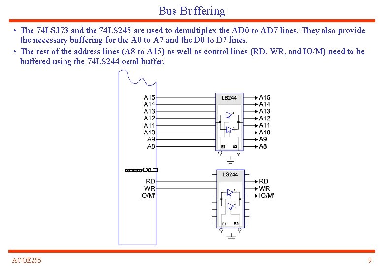
Bus Buffering • The 74 LS 373 and the 74 LS 245 are used to demultiplex the AD 0 to AD 7 lines. They also provide the necessary buffering for the A 0 to A 7 and the D 0 to D 7 lines. • The rest of the address lines (A 8 to A 15) as well as control lines (RD, WR, and IO/M) need to be buffered using the 74 LS 244 octal buffer. ACOE 255 9

A fully buffered/demultiplexed 8088 system ACOE 255 10

A fully buffered/demultiplexed 8086 system • The main difference with the 8086 processor is that it has a 16 -bit data bus multiplexed with the 16 lower address lines. – Thus the 16 -bit data bus (AD 0 to AD 7 and AD 8 to AD 15) must be demultiplexed. ACOE 255 11

BASIC BUS OPERATION • The 8086/88 processors use the memory and I/O in periods called bus cycles • Each bus cycle equals four system-clocking periods (T 1 -T 4) • For a 5 MHz clock, one bus cycle lasts 800 ns ACOE 255 12

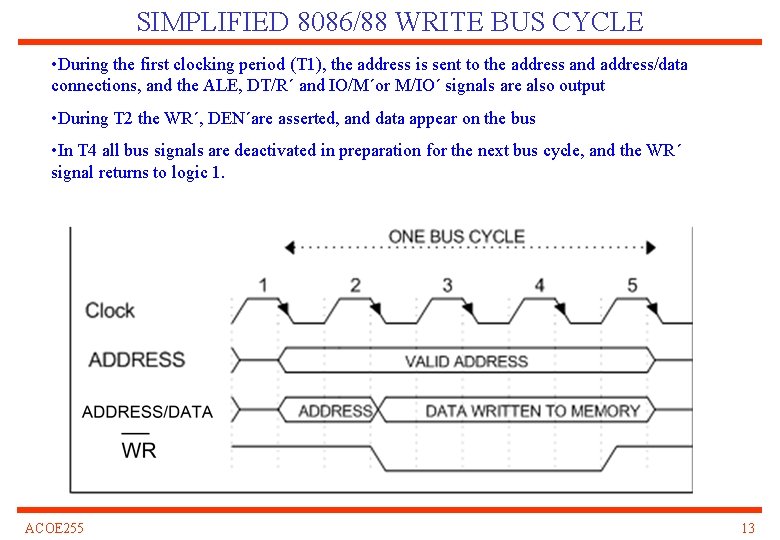
SIMPLIFIED 8086/88 WRITE BUS CYCLE • During the first clocking period (T 1), the address is sent to the address and address/data connections, and the ALE, DT/R΄ and IO/M΄or M/ΙΟ΄ signals are also output • During T 2 the WR΄, DEN΄are asserted, and data appear on the bus • In T 4 all bus signals are deactivated in preparation for the next bus cycle, and the WR΄ signal returns to logic 1. ACOE 255 13

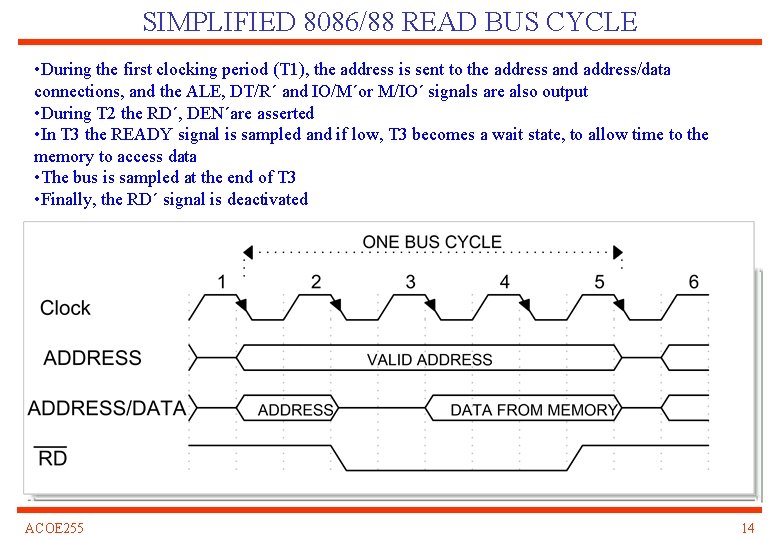
SIMPLIFIED 8086/88 READ BUS CYCLE • During the first clocking period (T 1), the address is sent to the address and address/data connections, and the ALE, DT/R΄ and IO/M΄or M/ΙΟ΄ signals are also output • During T 2 the RD΄, DEN΄are asserted • In T 3 the READY signal is sampled and if low, T 3 becomes a wait state, to allow time to the memory to access data • The bus is sampled at the end of T 3 • Finally, the RD΄ signal is deactivated ACOE 255 14

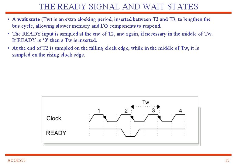
THE READY SIGNAL AND WAIT STATES • A wait state (Tw) is an extra clocking period, inserted between T 2 and T 3, to lengthen the bus cycle, allowing slower memory and I/O components to respond. • The READY input is sampled at the end of T 2, and again, if necessary in the middle of Tw. If READY is ‘ 0’ then a Tw is inserted. • At the end of T 2 is sampled on the falling clock edge, while in the middle of Tw, it is sampled on the rising clock edge. ACOE 255 15

Wait state generator circuit • Wait states are extra clock pulses inserted when the processor is accessing slow memory or I/O devices. • The 8088/8086 allow approximately 3 clock pulses for a memory read or memory write. If the access time of the memory (including the delays inserted by the bus buffers and address decoders) is longer than the access time of the processor (3/f) then wait states are needed. • The circuit shown adds 1 wait state in each memory read or write cycle. The number of wait states can be changed by changing the position of the jumper on the outputs of the 74 LS 164 shift register. ACOE 255 16