ADC specs and standard test 1 GAIN AND


- Slides: 102

ADC specs and standard test 1

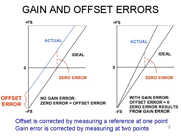
GAIN AND OFFSET ERRORS Offset is corrected by measuring a reference at one point 2 Gain error is corrected by measuring at two points

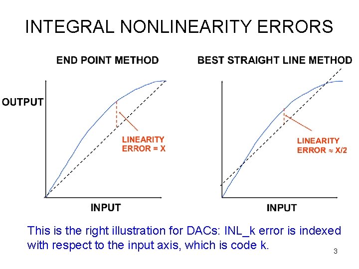
INTEGRAL NONLINEARITY ERRORS This is the right illustration for DACs: INL_k error is indexed with respect to the input axis, which is code k. 3

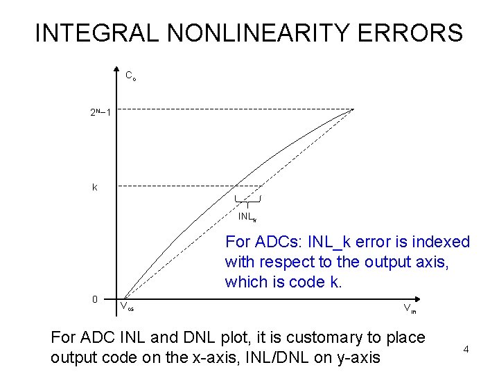
INTEGRAL NONLINEARITY ERRORS Co 2 N− 1 k INLk For ADCs: INL_k error is indexed with respect to the output axis, which is code k. 0 Vos Vin For ADC INL and DNL plot, it is customary to place output code on the x-axis, INL/DNL on y-axis 4

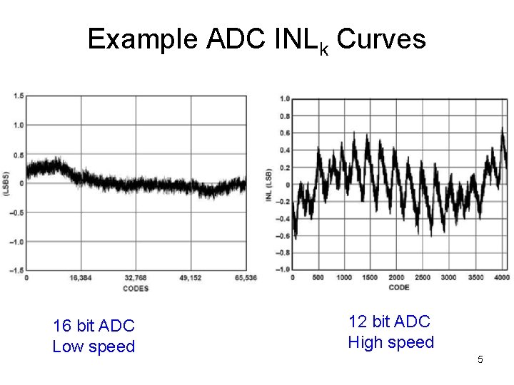
Example ADC INLk Curves 16 bit ADC Low speed 12 bit ADC High speed 5

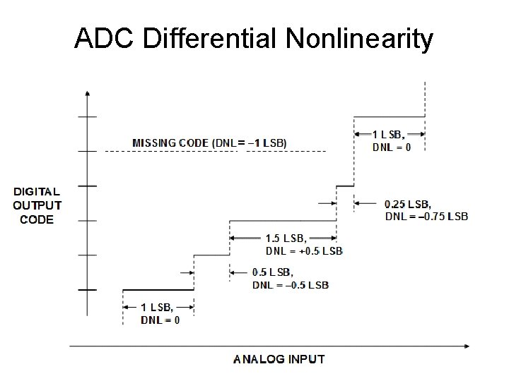
ADC Differential Nonlinearity = 6

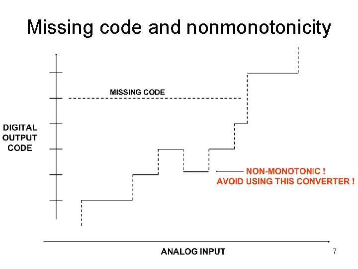
Missing code and nonmonotonicity 7

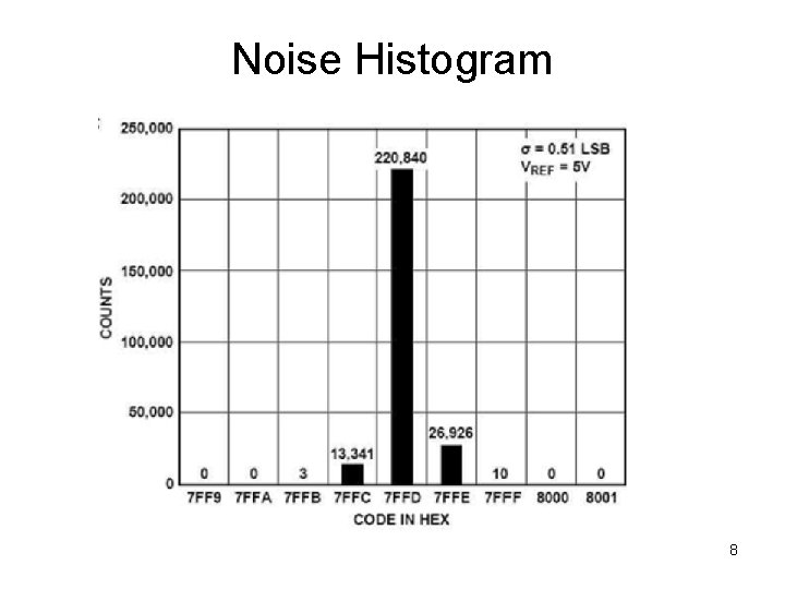
Noise Histogram 8

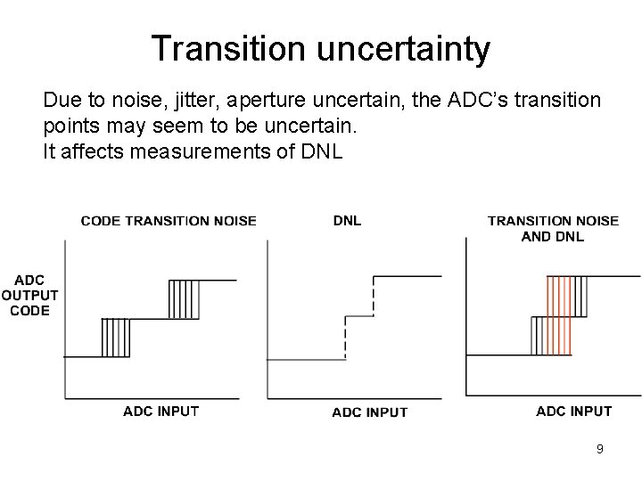
Transition uncertainty Due to noise, jitter, aperture uncertain, the ADC’s transition points may seem to be uncertain. It affects measurements of DNL 9

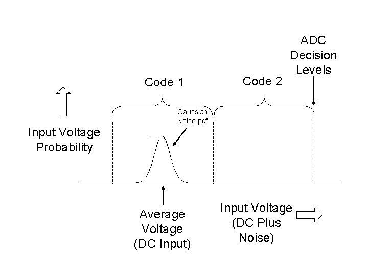
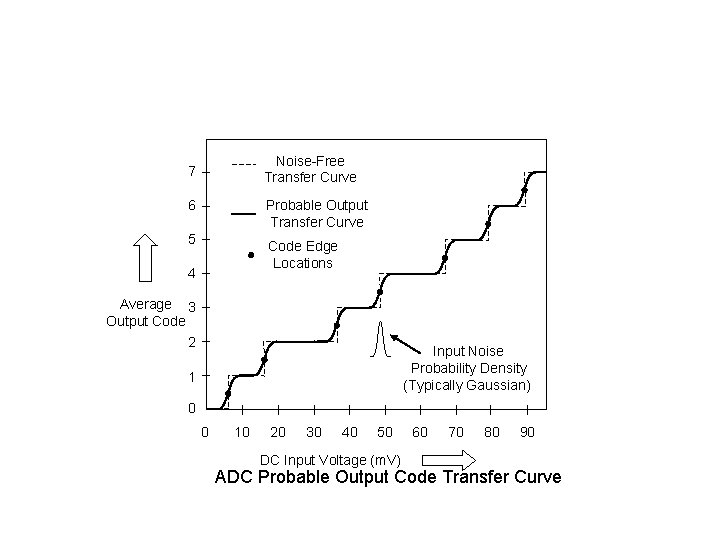
Code 1 Code 2 ADC Decision Levels Gaussian Noise pdf Input Voltage Probability Average Voltage (DC Input) Input Voltage (DC Plus Noise)

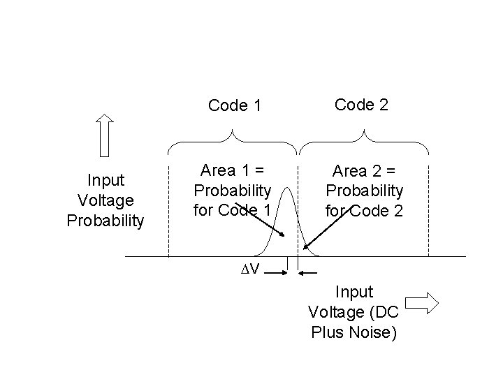
Input Voltage Probability Code 1 Code 2 Area 1 = Probability for Code 1 Area 2 = Probability for Code 2 DV Input Voltage (DC Plus Noise)

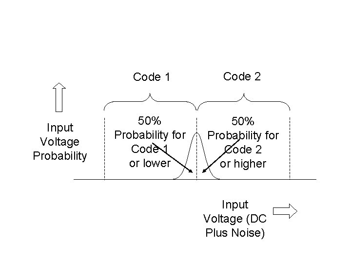
Input Voltage Probability Code 1 Code 2 50% Probability for Code 1 or lower 50% Probability for Code 2 or higher Input Voltage (DC Plus Noise)

Noise-Free Transfer Curve 7 6 Probable Output Transfer Curve 5 Code Edge Locations 4 Average 3 Output Code 2 Input Noise Probability Density (Typically Gaussian) 1 0 0 10 20 30 40 50 DC Input Voltage (m. V) 60 70 80 90 ADC Probable Output Code Transfer Curve

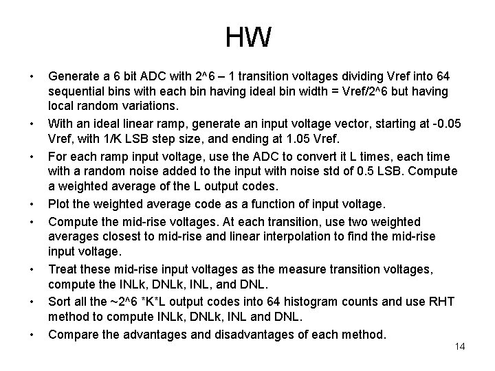
HW • • Generate a 6 bit ADC with 2^6 – 1 transition voltages dividing Vref into 64 sequential bins with each bin having ideal bin width = Vref/2^6 but having local random variations. With an ideal linear ramp, generate an input voltage vector, starting at -0. 05 Vref, with 1/K LSB step size, and ending at 1. 05 Vref. For each ramp input voltage, use the ADC to convert it L times, each time with a random noise added to the input with noise std of 0. 5 LSB. Compute a weighted average of the L output codes. Plot the weighted average code as a function of input voltage. Compute the mid-rise voltages. At each transition, use two weighted averages closest to mid-rise and linear interpolation to find the mid-rise input voltage. Treat these mid-rise input voltages as the measure transition voltages, compute the INLk, DNLk, INL, and DNL. Sort all the ~2^6 *K*L output codes into 64 histogram counts and use RHT method to compute INLk, DNLk, INL and DNL. Compare the advantages and disadvantages of each method. 14

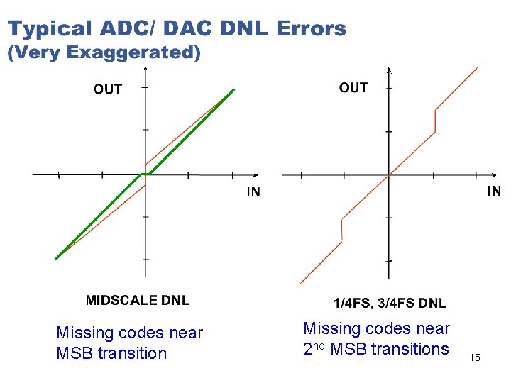
Missing codes near MSB transition Missing codes near 2 nd MSB transitions 15

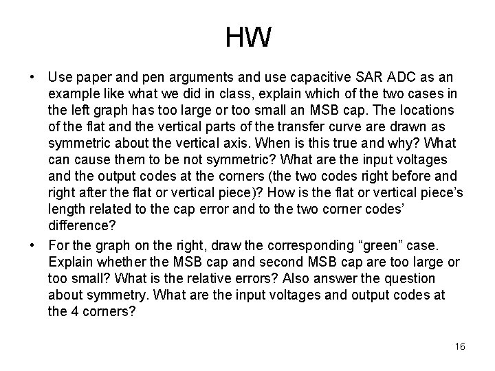
HW • Use paper and pen arguments and use capacitive SAR ADC as an example like what we did in class, explain which of the two cases in the left graph has too large or too small an MSB cap. The locations of the flat and the vertical parts of the transfer curve are drawn as symmetric about the vertical axis. When is this true and why? What can cause them to be not symmetric? What are the input voltages and the output codes at the corners (the two codes right before and right after the flat or vertical piece)? How is the flat or vertical piece’s length related to the cap error and to the two corner codes’ difference? • For the graph on the right, draw the corresponding “green” case. Explain whether the MSB cap and second MSB cap are too large or too small? What is the relative errors? Also answer the question about symmetry. What are the input voltages and output codes at the 4 corners? 16

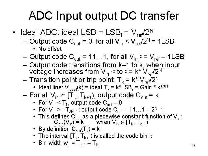
ADC Input output DC transfer • Ideal ADC: ideal LSB = LSBi = Vref/2 N – Output code Cout = 0, for all Vin < Vref/2 N = 1 LSB; • No offset – Output code Cout = 11… 1, for all Vin >= Vref – 1 LSB – Output code transitions from k– 1 to k, when input voltage increases from Vin < to >= k* Vref/2 N – Transition point or trip point: Tk = k* Vref/2 N • Ideal line: Videal(k) = ideal Tk = k*LSBi = Gain * k/2 N – For all Vin [Tk, Tk+1), output code Cout = k • For Vin < T 1, output code Cout = 0 • For Vin >= T 2 N– 1; output code Cout = 11… 1 = 2 N– 1 • This defines Cout as a piecewise constant function of Vin: Cout(Vin) = k when Vin [Tk, Tk+1) • By definition Cout(Tk) = k • The interval [Tk, Tk+1) is called the code bin k • Bin width wk = Tk+1 – Tk 17

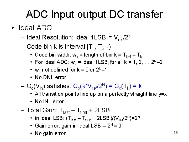
ADC Input output DC transfer • Ideal ADC: – Ideal Resolution: ideal 1 LSBi = Vref/2 N, – Code bin k is interval [Tk, Tk+1) • • Code bin width: wk = length of bin k = Tk+1 – Tk For ideal ADC: wk = ideal 1 LSBi for all k = 1, 2, … 2 N– 2 wk not defined for k = 0 or 2 N– 1 No DNL error – Co(Vin) satisfies: Co(k*Vref/2 N) = Co(Tk) = k • All transition points line up on a perfectly straight line y=x • No INL error – Total Gain: Tlast – Tfirst + 2 LSBi • in ideal LSB: (Tlast – Tfirst + 2 LSBi)/(Vref/2 N)=2 N • Gain error: gain in ideal LSBi – 2 N = 0 • No gain error 18

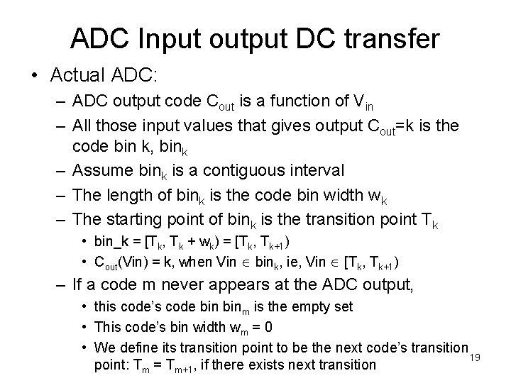
ADC Input output DC transfer • Actual ADC: – ADC output code Cout is a function of Vin – All those input values that gives output Cout=k is the code bin k, bink – Assume bink is a contiguous interval – The length of bink is the code bin width wk – The starting point of bink is the transition point Tk • bin_k = [Tk, Tk + wk) = [Tk, Tk+1) • Cout(Vin) = k, when Vin bink, ie, Vin [Tk, Tk+1) – If a code m never appears at the ADC output, • this code’s code binm is the empty set • This code’s bin width wm = 0 • We define its transition point to be the next code’s transition 19 point: Tm = Tm+1, if there exists next transition

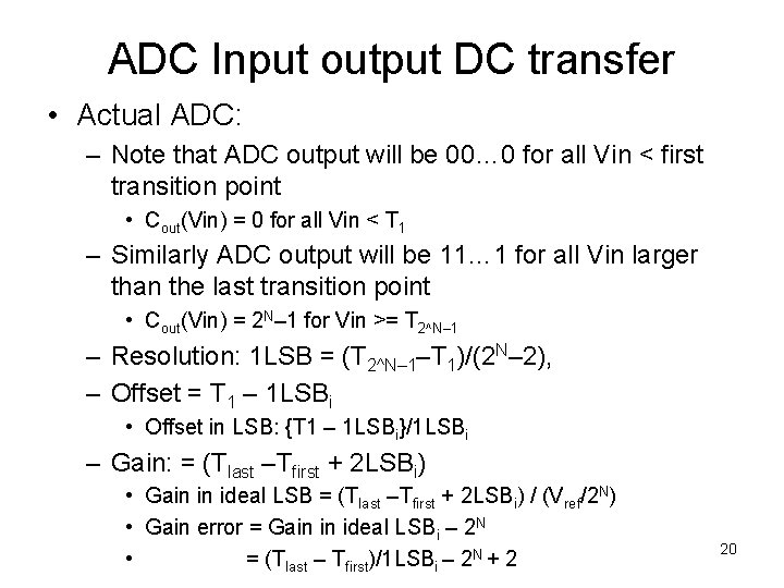
ADC Input output DC transfer • Actual ADC: – Note that ADC output will be 00… 0 for all Vin < first transition point • Cout(Vin) = 0 for all Vin < T 1 – Similarly ADC output will be 11… 1 for all Vin larger than the last transition point • Cout(Vin) = 2 N– 1 for Vin >= T 2^N– 1 – Resolution: 1 LSB = (T 2^N– 1–T 1)/(2 N– 2), – Offset = T 1 – 1 LSBi • Offset in LSB: {T 1 – 1 LSBi}/1 LSBi – Gain: = (Tlast –Tfirst + 2 LSBi) • Gain in ideal LSB = (Tlast –Tfirst + 2 LSBi) / (Vref/2 N) • Gain error = Gain in ideal LSBi – 2 N • = (Tlast – Tfirst)/1 LSBi – 2 N + 2 20

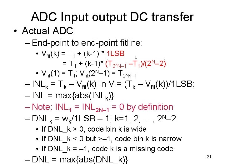
ADC Input output DC transfer • Actual ADC – End-point to end-point fitline: • Vfit(k) = T 1 + (k-1) * 1 LSB = T 1 + (k-1)* (T 2^N– 1 –T 1)/(2 N– 2) • Vfit(1) = T 1; Vfit(2 N– 1) = T 2^N– 1 – INLk = Tk – Vfit(k) in V = (Tk – Vfit(k))/1 LSB; – INL = max{abs(INLk)} – Note: INL 1 = INL 2 N– 1 = 0 by definition – DNLk = wk/1 LSB – 1; k=1, 2, …, 2 N– 2 • If DNL_k > 0, code bin k is wide • If DNL_k < 0 but >– 1, code bin k is narrow • If DNL_k = – 1, code k is a missing code – DNL = max{abs(DNL_k)} 21

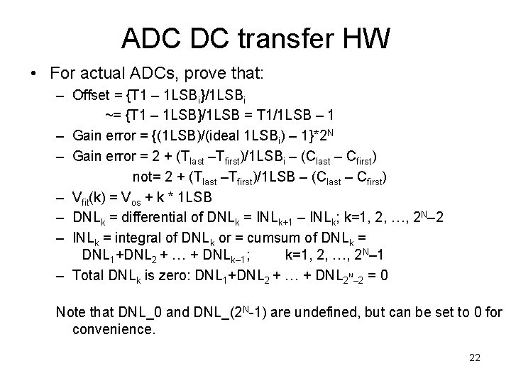
ADC DC transfer HW • For actual ADCs, prove that: – Offset = {T 1 – 1 LSBi}/1 LSBi ~= {T 1 – 1 LSB}/1 LSB = T 1/1 LSB – 1 – Gain error = {(1 LSB)/(ideal 1 LSBi) – 1}*2 N – Gain error = 2 + (Tlast –Tfirst)/1 LSBi – (Clast – Cfirst) not= 2 + (Tlast –Tfirst)/1 LSB – (Clast – Cfirst) – Vfit(k) = Vos + k * 1 LSB – DNLk = differential of DNLk = INLk+1 – INLk; k=1, 2, …, 2 N– 2 – INLk = integral of DNLk or = cumsum of DNLk = DNL 1+DNL 2 + … + DNLk– 1; k=1, 2, …, 2 N– 1 – Total DNLk is zero: DNL 1+DNL 2 + … + DNL 2 N– 2 = 0 Note that DNL_0 and DNL_(2 N-1) are undefined, but can be set to 0 for convenience. 22

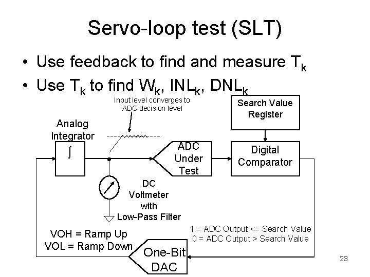
Servo-loop test (SLT) • Use feedback to find and measure Tk • Use Tk to find Wk, INLk, DNLk Input level converges to ADC decision level Analog Integrator ADC Under Test Search Value Register Digital Comparator DC Voltmeter with Low-Pass Filter VOH = Ramp Up VOL = Ramp Down 1 = ADC Output <= Search Value 0 = ADC Output > Search Value One-Bit DAC 23

SLT • SLT takes a long time to finish • Stationarity of the test environment becomes a significant issue • Even partial code test may require a time long enough to cause stationarity concerns • Solution is to repeatedly re-measure offset and gain error throughout SLT, and adjust Tk according to the latest measurement of offset and gain error 24

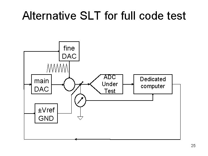
Alternative SLT for full code test fine DAC main DAC ADC Under Test Dedicated computer ±Vref GND 25

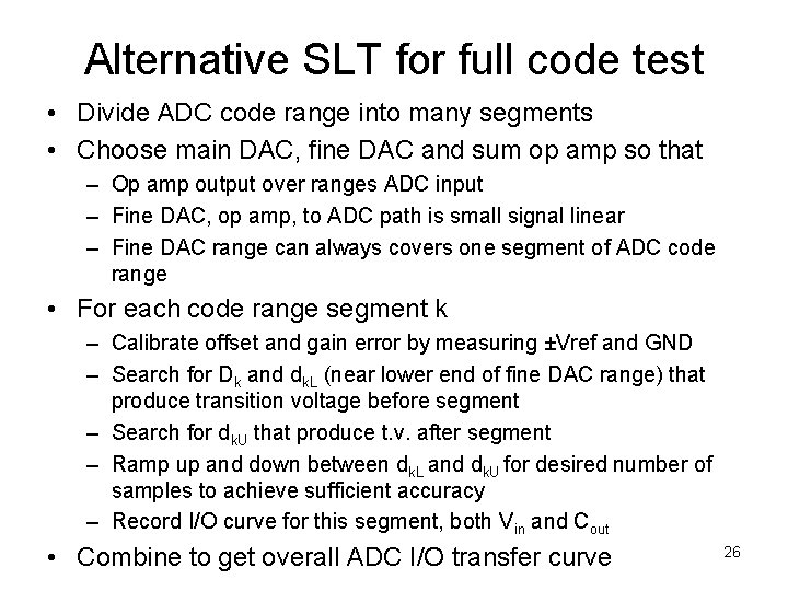
Alternative SLT for full code test • Divide ADC code range into many segments • Choose main DAC, fine DAC and sum op amp so that – Op amp output over ranges ADC input – Fine DAC, op amp, to ADC path is small signal linear – Fine DAC range can always covers one segment of ADC code range • For each code range segment k – Calibrate offset and gain error by measuring ±Vref and GND – Search for Dk and dk. L (near lower end of fine DAC range) that produce transition voltage before segment – Search for dk. U that produce t. v. after segment – Ramp up and down between dk. L and dk. U for desired number of samples to achieve sufficient accuracy – Record I/O curve for this segment, both Vin and Cout • Combine to get overall ADC I/O transfer curve 26

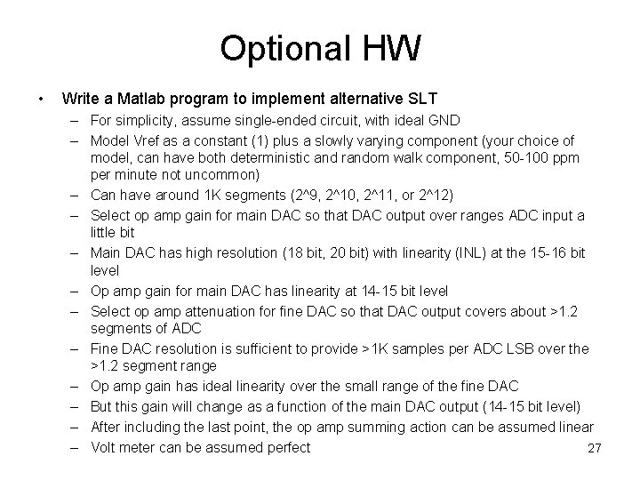
Optional HW • Write a Matlab program to implement alternative SLT – For simplicity, assume single-ended circuit, with ideal GND – Model Vref as a constant (1) plus a slowly varying component (your choice of model, can have both deterministic and random walk component, 50 -100 ppm per minute not uncommon) – Can have around 1 K segments (2^9, 2^10, 2^11, or 2^12) – Select op amp gain for main DAC so that DAC output over ranges ADC input a little bit – Main DAC has high resolution (18 bit, 20 bit) with linearity (INL) at the 15 -16 bit level – Op amp gain for main DAC has linearity at 14 -15 bit level – Select op amp attenuation for fine DAC so that DAC output covers about >1. 2 segments of ADC – Fine DAC resolution is sufficient to provide >1 K samples per ADC LSB over the >1. 2 segment range – Op amp gain has ideal linearity over the small range of the fine DAC – But this gain will change as a function of the main DAC output (14 -15 bit level) – After including the last point, the op amp summing action can be assumed linear 27 – Volt meter can be assumed perfect

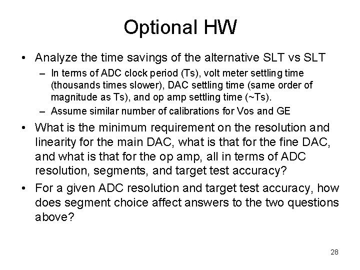
Optional HW • Analyze the time savings of the alternative SLT vs SLT – In terms of ADC clock period (Ts), volt meter settling time (thousands times slower), DAC settling time (same order of magnitude as Ts), and op amp settling time (~Ts). – Assume similar number of calibrations for Vos and GE • What is the minimum requirement on the resolution and linearity for the main DAC, what is that for the fine DAC, and what is that for the op amp, all in terms of ADC resolution, segments, and target test accuracy? • For a given ADC resolution and target test accuracy, how does segment choice affect answers to the two questions above? 28

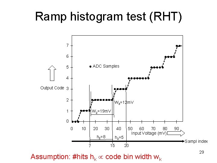
Ramp histogram test (RHT) 7 6 ADC Samples 5 4 Output Code 3 2 W 3=12 m. V 1 W 2=19 m. V 0 0 10 20 30 40 h 2=8 7 h 2=5 15 50 60 70 80 Input Voltage (m. V) 20 Assumption: #hits hk code bin width wk 90 Sampl index 29

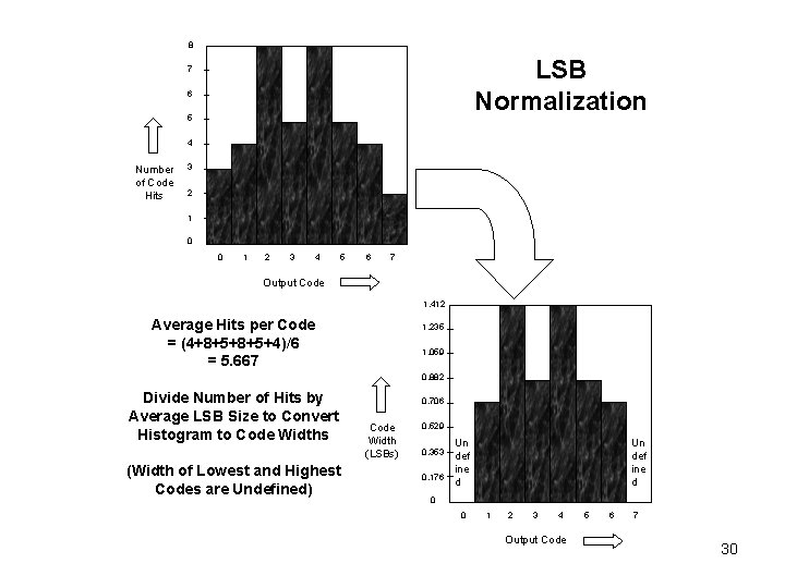
8 LSB Normalization 7 6 5 4 Number of Code Hits 3 2 1 0 0 1 2 3 4 5 6 7 Output Code 1. 412 Average Hits per Code = (4+8+5+4)/6 = 5. 667 1. 235 1. 059 0. 882 Divide Number of Hits by Average LSB Size to Convert Histogram to Code Widths (Width of Lowest and Highest Codes are Undefined) 12 0. 706 Code Width (LSBs) 0. 529 0. 353 0. 176 Un def ine d 0 0 1 2 3 4 Output Code 5 6 7 30

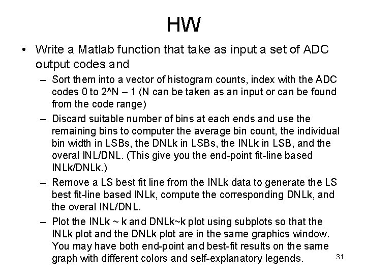
HW • Write a Matlab function that take as input a set of ADC output codes and – Sort them into a vector of histogram counts, index with the ADC codes 0 to 2^N – 1 (N can be taken as an input or can be found from the code range) – Discard suitable number of bins at each ends and use the remaining bins to computer the average bin count, the individual bin width in LSBs, the DNLk in LSBs, the INLk in LSB, and the overal INL/DNL. (This give you the end-point fit-line based INLk/DNLk. ) – Remove a LS best fit line from the INLk data to generate the LS best fit-line based INLk, compute the corresponding DNLk, and the overal INL/DNL. – Plot the INLk ~ k and DNLk~k plot using subplots so that the INLk plot and the DNLk plot are in the same graphics window. You may have both end-point and best-fit results on the same 31 graph with different colors and self-explanatory legends.

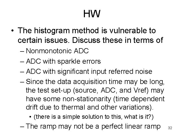
HW • The histogram method is vulnerable to certain issues. Discuss these in terms of – Nonmonotonic ADC – ADC with sparkle errors – ADC with significant input referred noise – Since the data acquisition time may be long, the test set-up (source, ADC, and Vref) may have some non-stationarity (time dependent drift due to thermal and other variations). • (there is a simple solution to this, what is it? ) – The ramp may not be a perfect linear ramp 32

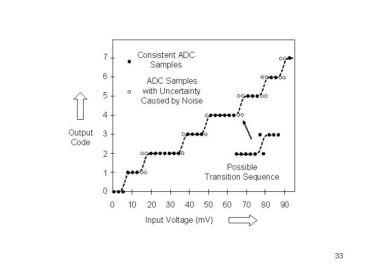
Consistent ADC Samples 7 6 ADC Samples with Uncertainty Caused by Noise 5 4 Output Code 3 2 Possible Transition Sequence 1 0 0 10 20 30 40 50 60 70 80 90 Input Voltage (m. V) 33

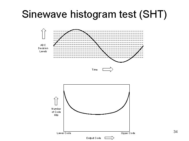
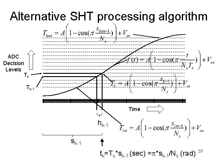
Sinewave histogram test (SHT) ADC Decision Levels Time Number of Code Hits Lower Code Upper Code Output Code 34

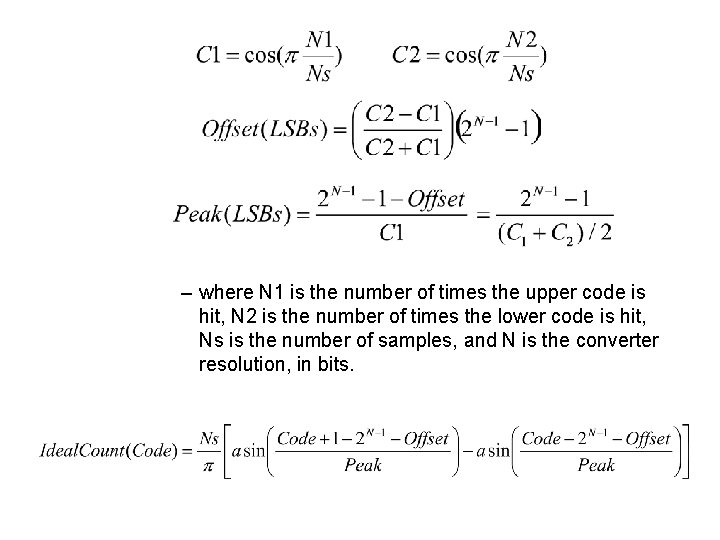
– where N 1 is the number of times the upper code is hit, N 2 is the number of times the lower code is hit, Ns is the number of samples, and N is the converter resolution, in bits.

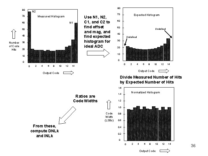
80 80 N 2 Measured Histogram 70 N 1 60 50 40 Number of Code Hits 30 20 Use N 1, N 2, C 1, and C 2 to find offset and mag, and find expected histogram for ideal ADC 70 Expected Histogram 60 50 Undefined 40 Undefined 30 20 10 10 0 0 2 0 4 6 8 10 12 0 14 2 4 6 8 10 12 14 Output Code Divide Measured Number of Hits by Expected Number of Hits 1. 6 Ratios are Code Widths 1. 2 1. 0 12 Code Width (LSBs) From these, compute DNLk and INLk Normalized Histogram 1. 4 0. 8 0. 6 0. 4 0. 2 0 12 0 2 4 6 8 10 Output Code 12 14 36

Alternative SHT processing algorithm ADC Decision Levels Tk Tk-1 Time hk-1 sk-1 tk=Ts*sk-1 (sec) =p*sk-1/Ns (rad) 37

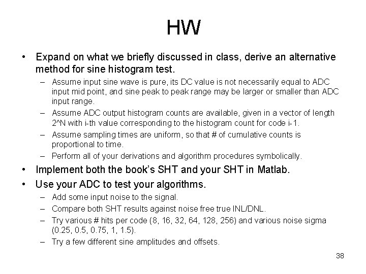
HW • Expand on what we briefly discussed in class, derive an alternative method for sine histogram test. – Assume input sine wave is pure, its DC value is not necessarily equal to ADC input mid point, and sine peak to peak range may be larger or smaller than ADC input range. – Assume ADC output histogram counts are available, given in a vector of length 2^N with i-th value corresponding to the histogram count for code i-1. – Assume sampling times are uniform, so that # of cumulative counts is proportional to time. – Perform all of your derivations and algorithm procedures symbolically. • Implement both the book’s SHT and your SHT in Matlab. • Use your ADC to test your algorithms. – Add some input noise to the signal. – Compare both SHT results against noise free true INL/DNL. – Try various # hits per code (8, 16, 32, 64, 128, 256) and various noise sigma (0. 25, 0. 75, 1, 1. 5). – Try a few different sine amplitudes and offsets. 38

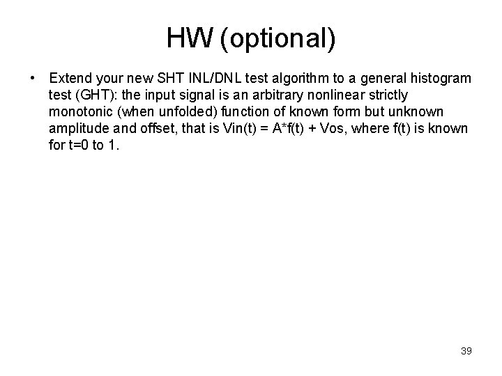
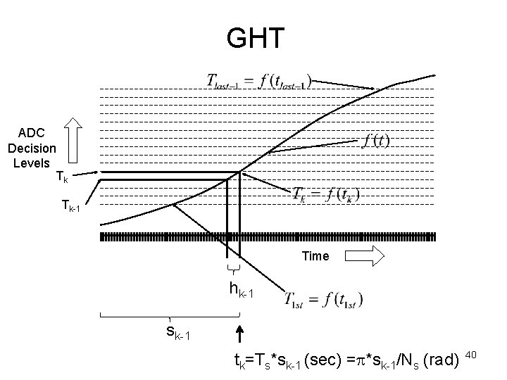
HW (optional) • Extend your new SHT INL/DNL test algorithm to a general histogram test (GHT): the input signal is an arbitrary nonlinear strictly monotonic (when unfolded) function of known form but unknown amplitude and offset, that is Vin(t) = A*f(t) + Vos, where f(t) is known for t=0 to 1. 39

GHT ADC Decision Levels Tk Tk-1 Time hk-1 sk-1 tk=Ts*sk-1 (sec) =p*sk-1/Ns (rad) 40

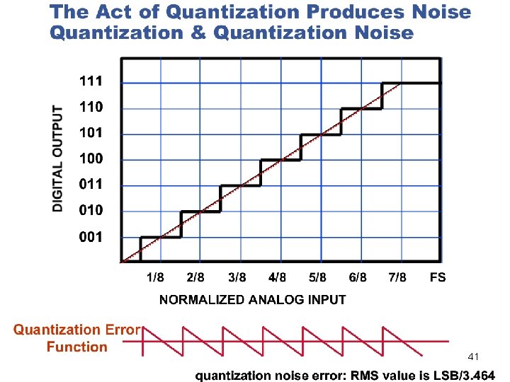
41

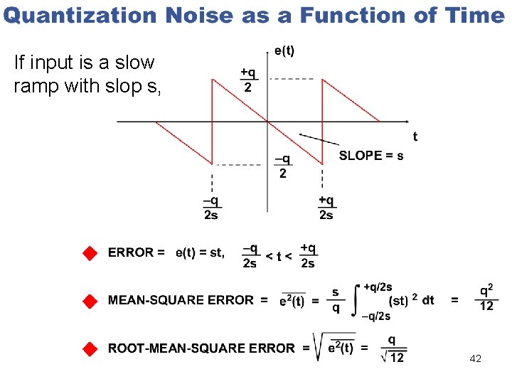
If input is a slow ramp with slop s, 42

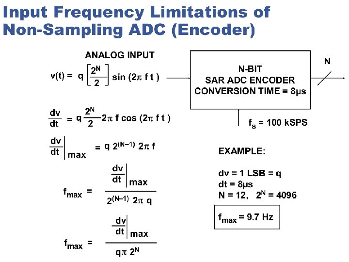
43

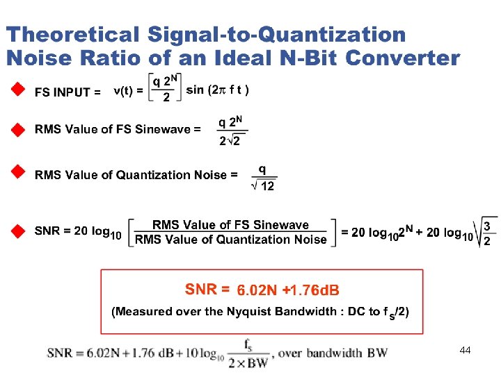
44

HW Assume that the ADC is non-ideal. In particular, DNL_k != 0. • Redefined the quantization error as a function of Vin, and define the correct expression of the mean square error. • Approximately estimate the ms error. • Re-compute the noise-free signal to quantization ratio. 45

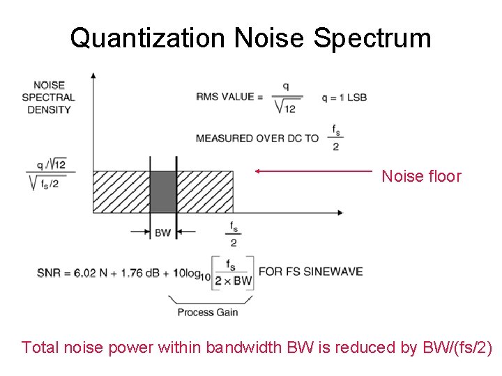
Quantization Noise Spectrum Noise floor Total noise power within bandwidth BW is reduced by BW/(fs/2) 46

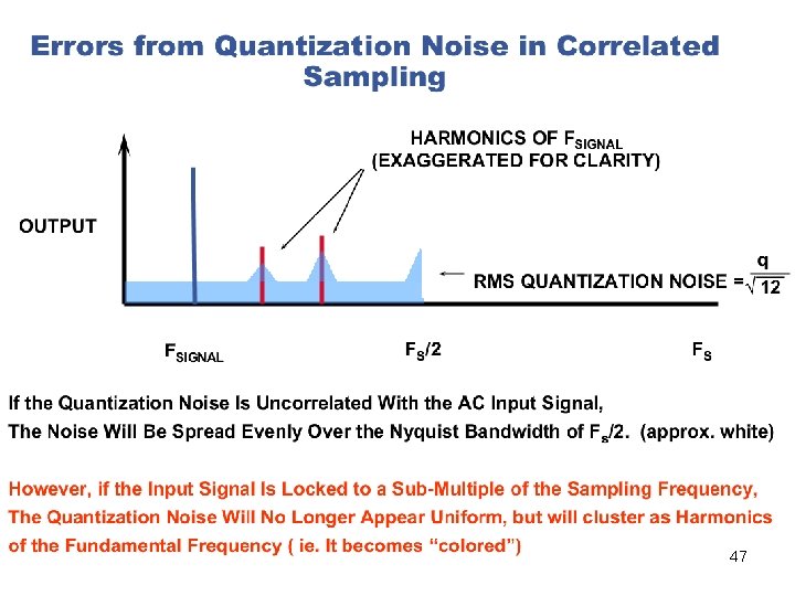
47

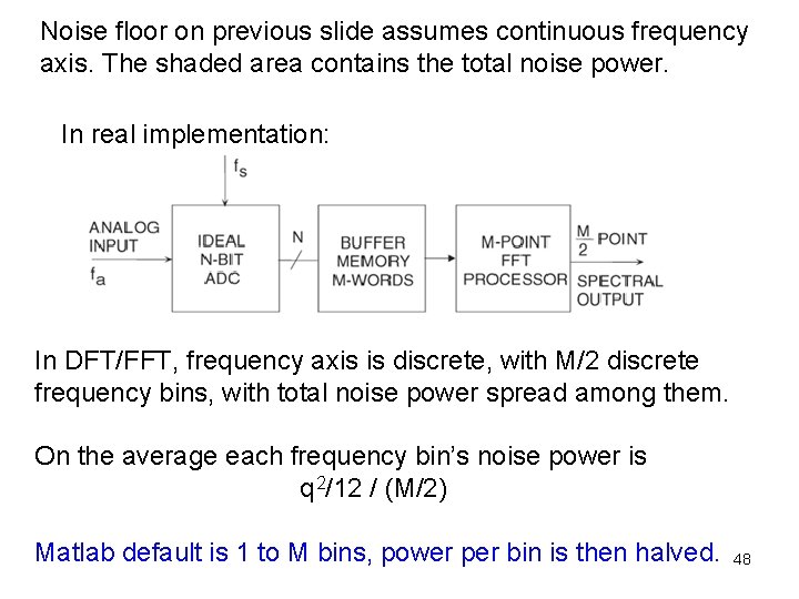
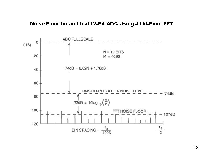
Noise floor on previous slide assumes continuous frequency axis. The shaded area contains the total noise power. In real implementation: In DFT/FFT, frequency axis is discrete, with M/2 discrete frequency bins, with total noise power spread among them. On the average each frequency bin’s noise power is q 2/12 / (M/2) Matlab default is 1 to M bins, power per bin is then halved. 48

Noise Floor for an Ideal 12 -Bit ADC Using 4096 -Point FFT 49

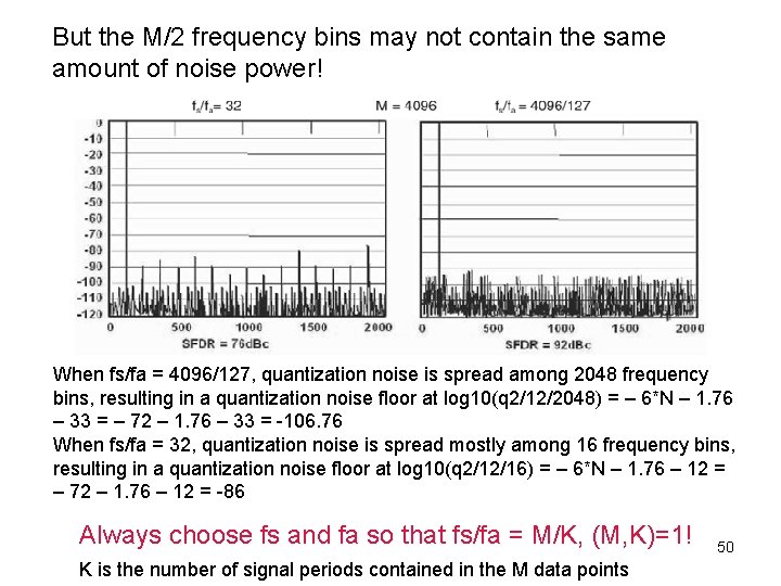
But the M/2 frequency bins may not contain the same amount of noise power! When fs/fa = 4096/127, quantization noise is spread among 2048 frequency bins, resulting in a quantization noise floor at log 10(q 2/12/2048) = – 6*N – 1. 76 – 33 = – 72 – 1. 76 – 33 = -106. 76 When fs/fa = 32, quantization noise is spread mostly among 16 frequency bins, resulting in a quantization noise floor at log 10(q 2/12/16) = – 6*N – 1. 76 – 12 = – 72 – 1. 76 – 12 = -86 Always choose fs and fa so that fs/fa = M/K, (M, K)=1! K is the number of signal periods contained in the M data points 50

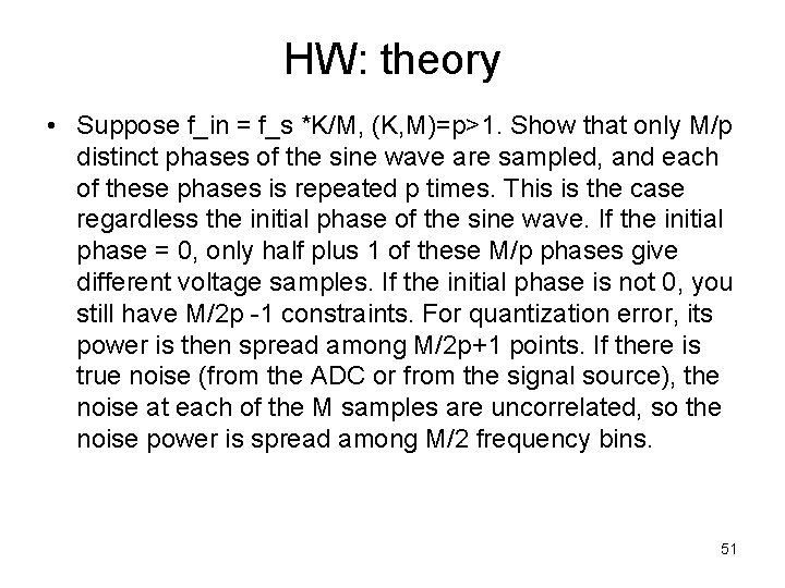
HW: theory • Suppose f_in = f_s *K/M, (K, M)=p>1. Show that only M/p distinct phases of the sine wave are sampled, and each of these phases is repeated p times. This is the case regardless the initial phase of the sine wave. If the initial phase = 0, only half plus 1 of these M/p phases give different voltage samples. If the initial phase is not 0, you still have M/2 p -1 constraints. For quantization error, its power is then spread among M/2 p+1 points. If there is true noise (from the ADC or from the signal source), the noise at each of the M samples are uncorrelated, so the noise power is spread among M/2 frequency bins. 51

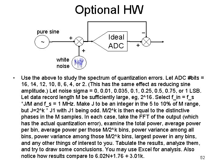
Optional HW pure sine ~ + + Ideal ADC – + white noise • Use the above to study the spectrum of quantization errors. Let ADC #bits = 16, 14, 12, 10, 8, 6, 4, or 2. (This has the same effect as reducing sine amplitude. ) Let noise sigma = 0, 0. 01, 0. 035, 0. 1, 0. 25, 0. 75, or 1 LSB. Let data record length M be sufficiently large, eg, 2^16. Select f_in = f_s *J/M and f_s = 1 MHz. Make J to be an integer in the 5 to 10% of M range, but J=2^k * J 1 with J 1 being odd. M/2^k is then equal to the distinctive phases in the M samples. In each case, take the FFT of the output (which has the actual quantization error), examine the total power, average power per bin, average power per those M/2^k bins, power variance among all bins, power variance among those M/2^k bins, largest power in any bins, and any other things of interest to you. Tabulate the results, analyze them, and try to draw some conclusions. You may use Excel for analysis. Also notice how results compare to 6. 02 N+1. 76 + 3. 01 k. 52

Coherent sampling • To ensure correct data collection and FFT, the signal frequency, clock frequency, the number of data points M used in FFT, and the number of signal periods K contained in the M points have to satisfy some stringent conditions: – – f_sampling : f_signal has to be rational f_s / f_sig = M / K = integer / integer M and K should be co-prime For efficient FFT, M is typically selected as an integer power of 2 – K is typically selected as an odd integer – IEEE says K should be at least 5 – This gives a signal frequency choice of f_sig = f_s *K/M 53

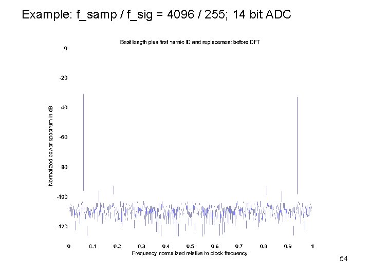
Example: f_samp / f_sig = 4096 / 255; 14 bit ADC 54

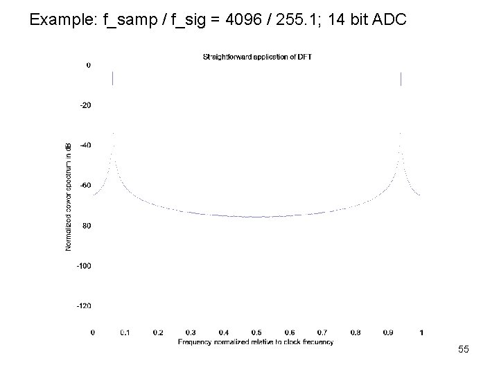
Example: f_samp / f_sig = 4096 / 255. 1; 14 bit ADC 55

Example: f_samp / f_sig = 4096 / 255. 01; 14 bit ADC 56

Example: f_samp / f_sig = 4096 / 255. 001; 14 bit ADC 57

HW • Use a 16 bit ideal ADC, Vref = +-1, M=2^16, J=Jint+d, fs=1, fin =J/M*fs, f=rand*2 p, Vos=0, and A = Vref. • For each Jint, find d such that Pleak Pnoise. You can simply take Pleak = Ptot – Psig – Pnoise. • For a given Jint and d, how does f affect Pleak? • Repeat the above for Jint near M/4, M/8, M/16, M/32, M/64, and M/128, but make sure round(J) is odd. (Use f=(rand-0. 5)*2 p) • Based on the above, can you draw a conclusion on the accuracy of frequency control to ensure negligible leakage? 58

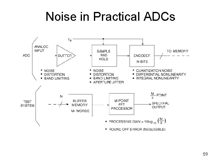
Noise in Practical ADCs 59

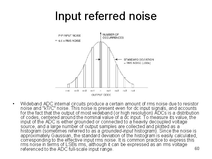
Input referred noise • Wideband ADC internal circuits produce a certain amount of rms noise due to resistor noise and "k. T/C" noise. This noise is present even for dc input signals, and accounts for the fact that the output of most wideband (or high resolution) ADCs is a distribution of codes, centered around the nominal value of a dc input. To measure its value, the input of the ADC is either grounded or connected to a heavily decoupled voltage source, and a large number of output samples are collected and plotted as a histogram (sometimes referred to as a grounded-input histogram). Since the noise is approximately Gaussian, the standard deviation of the histogram is easily calculated, corresponding to the effective input rms noise. It is common practice to express this rms noise in terms of LSBs rms, although it can be expressed as an rms voltage 60 referenced to the ADC full-scale input range.

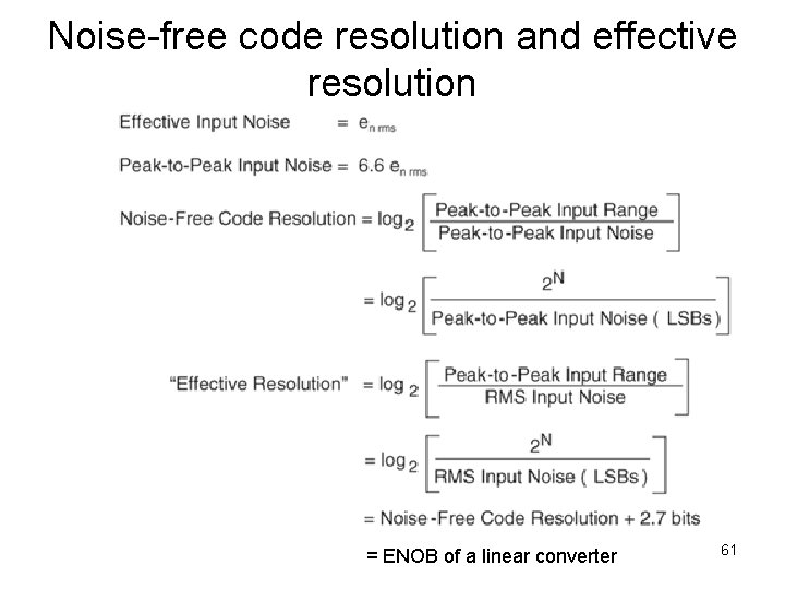
Noise-free code resolution and effective resolution = ENOB of a linear converter 61

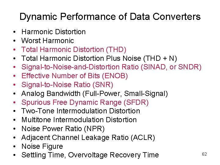
Dynamic Performance of Data Converters • • • • Harmonic Distortion Worst Harmonic Total Harmonic Distortion (THD) Total Harmonic Distortion Plus Noise (THD + N) Signal-to-Noise-and-Distortion Ratio (SINAD, or SNDR) Effective Number of Bits (ENOB) Signal-to-Noise Ratio (SNR) Analog Bandwidth (Full-Power, Small-Signal) Spurious Free Dynamic Range (SFDR) Two-Tone Intermodulation Distortion Multitone Intermodulation Distortion Noise Power Ratio (NPR) Adjacent Channel Leakage Ratio (ACLR) Noise Figure 62 Settling Time, Overvoltage Recovery Time

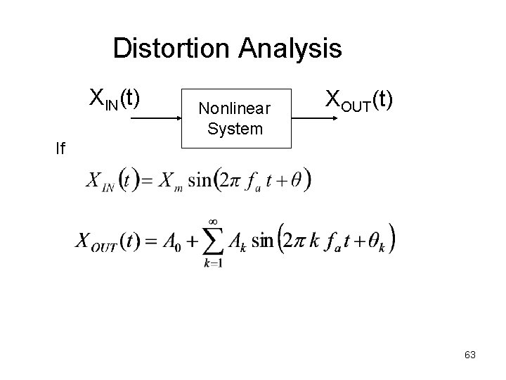
Distortion Analysis XIN(t) Nonlinear System XOUT(t) If 63

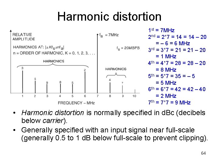
Harmonic distortion 1 st = 7 MHz 2 nd = 2*7 = 14 – 20 = – 6 = 6 MHz 3 rd = 3*7 = 21 – 20 = 1 MHz 4 th = 4*7 = 28 – 20 = 8 MHz 5 th = 5*7 = 35 = – 5 = 5 MHz 6 th = 6*7 = 42 – 40 = 2 MHz 7 th = 7*7 = 9 MHz • Harmonic distortion is normally specified in d. Bc (decibels below carrier). • Generally specified with an input signal near full-scale (generally 0. 5 to 1 d. B below full-scale to prevent clipping). 64

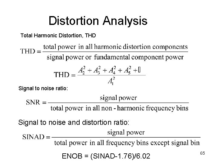
Distortion Analysis Total Harmonic Distortion, THD Signal to noise ratio: Signal to noise and distortion ratio: ENOB = (SINAD-1. 76)/6. 02 65

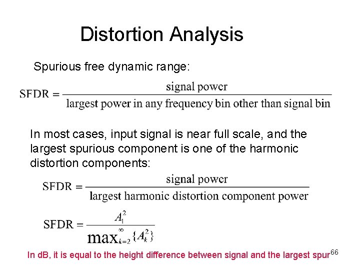
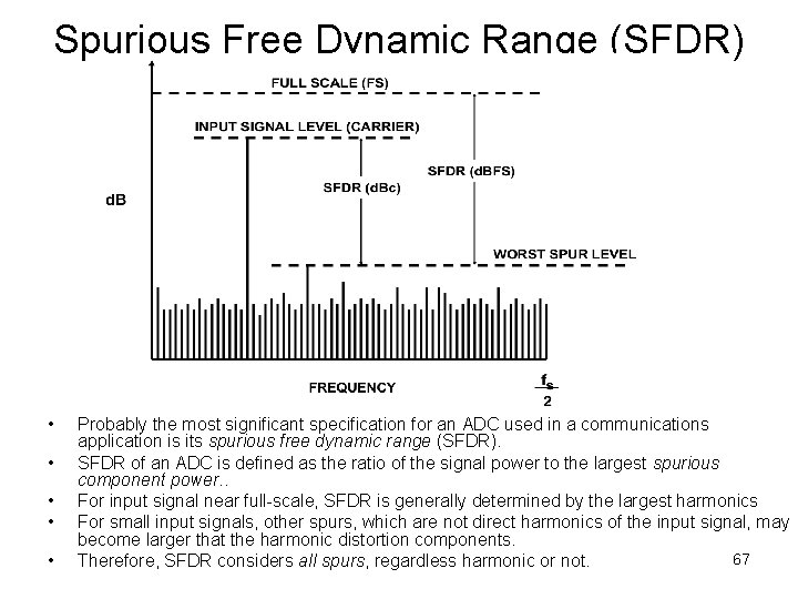
Distortion Analysis Spurious free dynamic range: In most cases, input signal is near full scale, and the largest spurious component is one of the harmonic distortion components: In d. B, it is equal to the height difference between signal and the largest spur 66

Spurious Free Dynamic Range (SFDR) • • • Probably the most significant specification for an ADC used in a communications application is its spurious free dynamic range (SFDR). SFDR of an ADC is defined as the ratio of the signal power to the largest spurious component power. . For input signal near full-scale, SFDR is generally determined by the largest harmonics For small input signals, other spurs, which are not direct harmonics of the input signal, may become larger that the harmonic distortion components. 67 Therefore, SFDR considers all spurs, regardless harmonic or not.

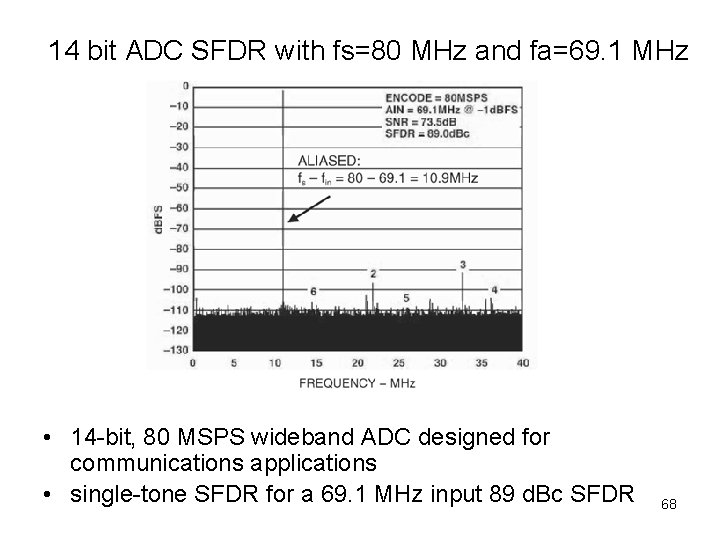
14 bit ADC SFDR with fs=80 MHz and fa=69. 1 MHz • 14 -bit, 80 MSPS wideband ADC designed for communications applications • single-tone SFDR for a 69. 1 MHz input 89 d. Bc SFDR 68

HW • • Write a Matlab function for single tone coherent spectral testing. The input is a vector of ADC output, containing M=2^m samples. It should compute and plot the whole spectrum, normalized with respect to (±Vref)^2. This is so as to easily show if the input sine wave is at attenuated power levels by displaying the signal power. When computing the signal power, you should include a few bins on each side of the fundamental. It should also compute and list the 2 nd to 10 th harmonic frequencies and harmonic distortion powers. In computing the harmonic distortion powers, you can include one or two extra bins on each side of the harmonic bin so as to capture the possible small amount of power leakage due to imperfect coherency. It should compute and display the SFDR and indicating if it is spurious, or if it is harmonic (and which one). In computing the THD, it should include up to the 20 th harmonic distortion powers. In computing the total noise power, the bins used for distortion powers should be excluded, and the remaining total noise power should be scaled up to correspond to M noise bins. 69 Also display SNR, SINAD, ENOB.

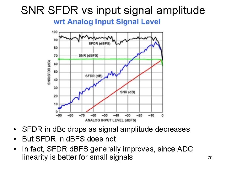
SNR SFDR vs input signal amplitude • SFDR in d. Bc drops as signal amplitude decreases • But SFDR in d. BFS does not • In fact, SFDR d. BFS generally improves, since ADC linearity is better for small signals 70

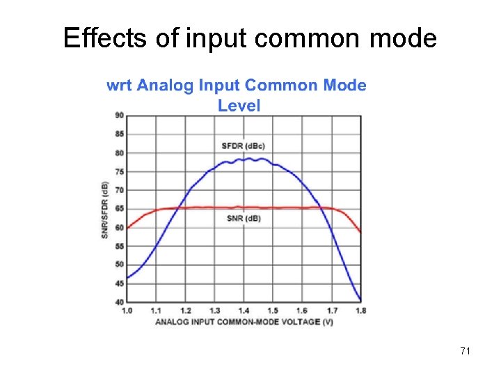
Effects of input common mode 71

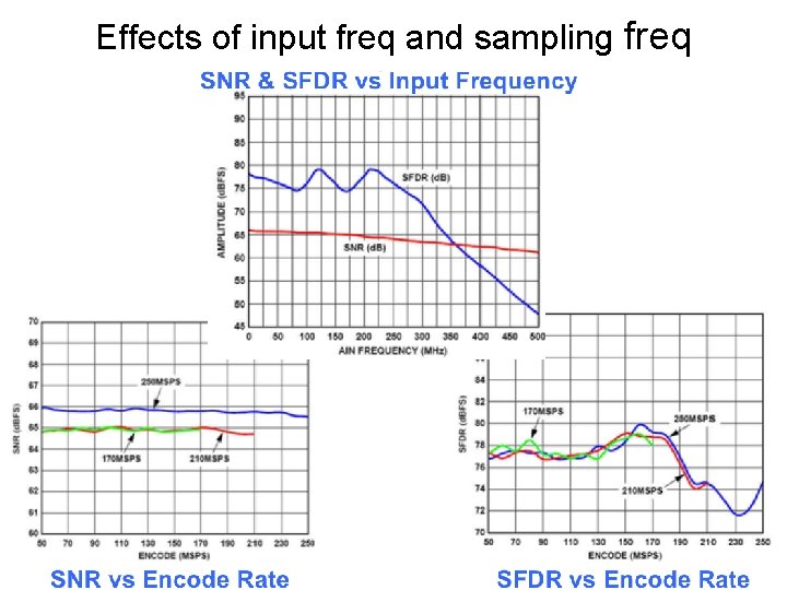
Effects of input freq and sampling freq 72

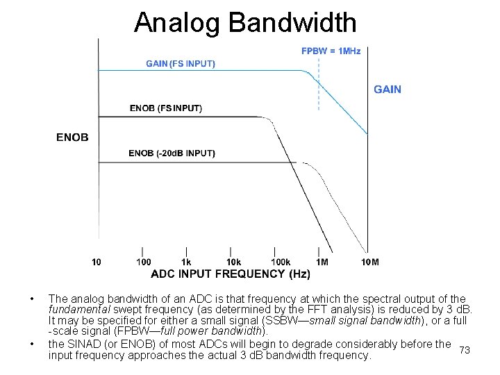
Analog Bandwidth • • The analog bandwidth of an ADC is that frequency at which the spectral output of the fundamental swept frequency (as determined by the FFT analysis) is reduced by 3 d. B. It may be specified for either a small signal (SSBW—small signal bandwidth), or a full -scale signal (FPBW—full power bandwidth). the SINAD (or ENOB) of most ADCs will begin to degrade considerably before the 73 input frequency approaches the actual 3 d. B bandwidth frequency.

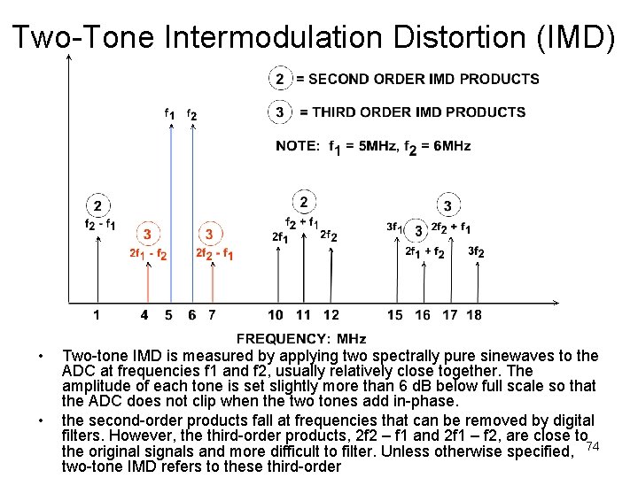
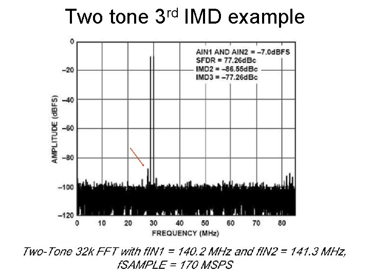
Two-Tone Intermodulation Distortion (IMD) • • Two-tone IMD is measured by applying two spectrally pure sinewaves to the ADC at frequencies f 1 and f 2, usually relatively close together. The amplitude of each tone is set slightly more than 6 d. B below full scale so that the ADC does not clip when the two tones add in-phase. the second-order products fall at frequencies that can be removed by digital filters. However, the third-order products, 2 f 2 – f 1 and 2 f 1 – f 2, are close to the original signals and more difficult to filter. Unless otherwise specified, 74 two-tone IMD refers to these third-order

Two tone 3 rd IMD example 75

HW • Write a Matlab function that takes as input a vector of ADC outputs sampled coherently in a two tone test, compute and plot its spectrum, and compute and display the k-th harmonic and intermodulation spectral components for k=0 to 10. (k=0 is DC) For the spectrum plot, normalize with respect to the total signal power. Set the lower limit of the vertical axis to 10 d. B below the total noise floor (rounded to the nearest d. B). Your program should also check if any of the two rails of the ADC was hit and give an warning if it was. Finally, the peak positive amplitude and peak negative amplitude should be computed and compared to the rms value. 76

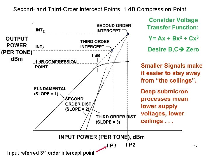
Second- and Third-Order Intercept Points, 1 d. B Compression Point IIP 3 Input referred 3 rd order intercept point IIP 2 77

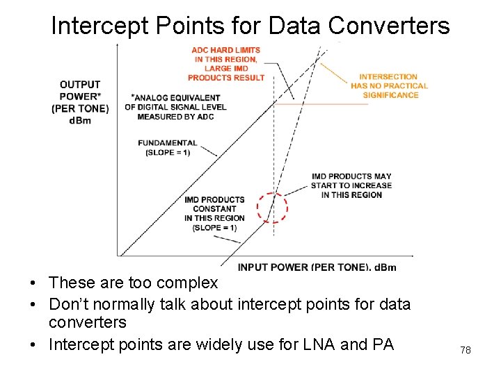
Intercept Points for Data Converters • These are too complex • Don’t normally talk about intercept points for data converters • Intercept points are widely use for LNA and PA 78

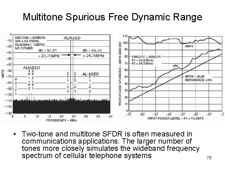
Multitone Spurious Free Dynamic Range • Two-tone and multitone SFDR is often measured in communications applications. The larger number of tones more closely simulates the wideband frequency spectrum of cellular telephone systems 79

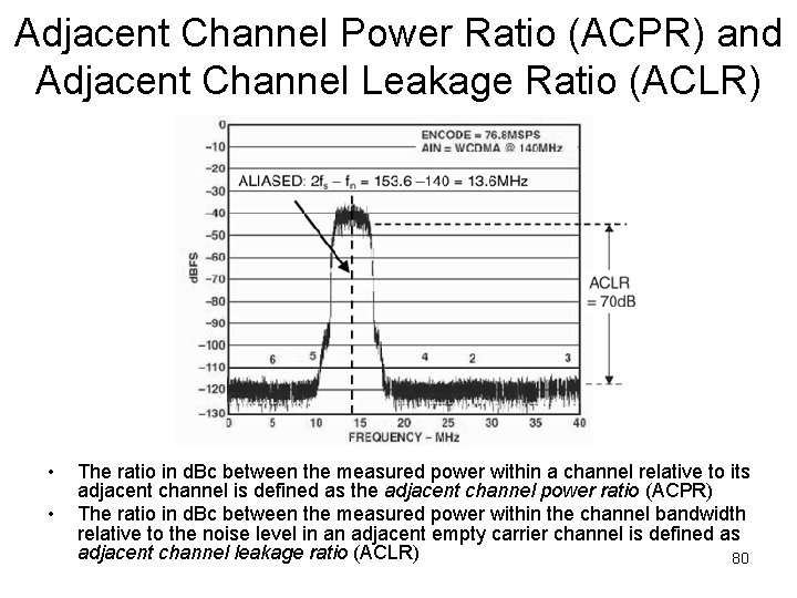
Adjacent Channel Power Ratio (ACPR) and Adjacent Channel Leakage Ratio (ACLR) • • The ratio in d. Bc between the measured power within a channel relative to its adjacent channel is defined as the adjacent channel power ratio (ACPR) The ratio in d. Bc between the measured power within the channel bandwidth relative to the noise level in an adjacent empty carrier channel is defined as adjacent channel leakage ratio (ACLR) 80

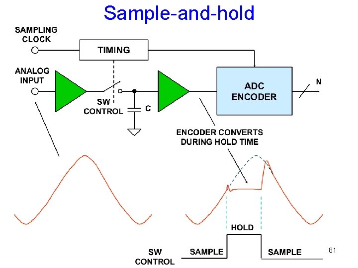
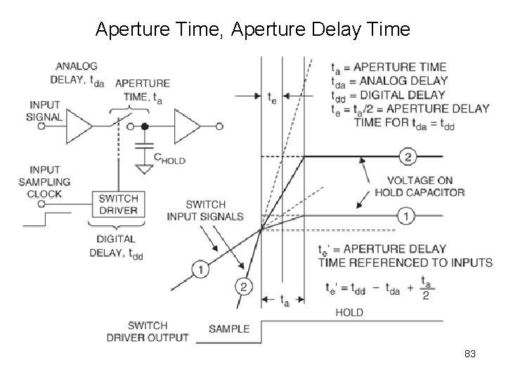
Sample-and-hold 81

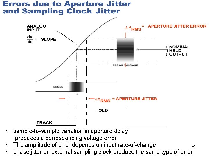
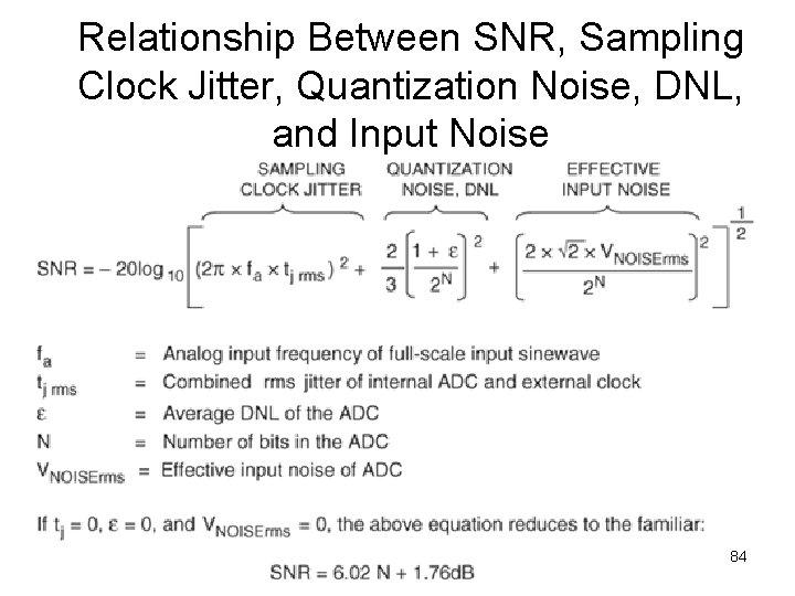
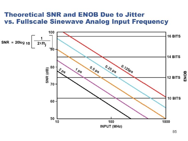
• sample-to-sample variation in aperture delay produces a corresponding voltage error • The amplitude of error depends on input rate-of-change 82 • phase jitter on external sampling clock produce the same type of error

Aperture Time, Aperture Delay Time 83

Relationship Between SNR, Sampling Clock Jitter, Quantization Noise, DNL, and Input Noise 84

85

HW • Use an ideal high resolution ADC (rounding at 10^-9 is about 30 bits), with sampling frequency of 2 GHz (No body has such an ADC, and no body will). Use an ideal sine wave input with full scale, no offset, and no noise. The sampling clock has independent clock jitter at each sampling instant. • Generate a graph that is similar to the previous slide. Make the horizontal axis from 100 KHz to 1 GHz, and the vertical axis 50 to 120 d. B and 8 bits to 20 bits. Use the same 5 jitter amounts. 86

HW • Spend some time with Matlab’s Help facility. • Find out a list of all the available built-in window functions, make a plot of the time domain and spectral domain shape of each window in its default form, find the d. B difference between the peak of the main lobe and the peak of the secondary lobes, find the critical things one needs to pay attention to in order to use each window correctly, and find the limitations on the SNR and THD measurement accuracies of each window. 87

HW • Write a Matlab program to demonstrate the use of the Blackman. Harris window in high resolution ADC spectral testing. • Use your SAR ADC with 16, 18, or 20 bit resolution. • Use a data record length of 2^14, 2^15, or 2^16. • Use a pure input sine wave, with correct DC and -0. 5 d. BFS. • Use a randomly generated frequency so that the number of signal period in the data record is in the range of 1/20 to 1/3 of the number of samples. • For each test case, test the ADC with perfectly coherent sampling, test again with non-coherent sampling plus windowing, and compare the test results in SNR, THD, and SFDR. 88

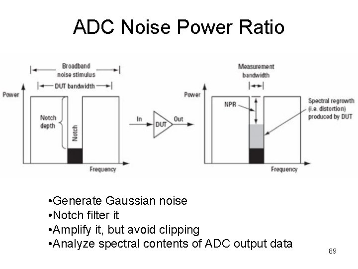
ADC Noise Power Ratio • Generate Gaussian noise • Notch filter it • Amplify it, but avoid clipping • Analyze spectral contents of ADC output data 89

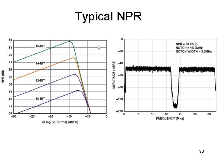
Typical NPR 90

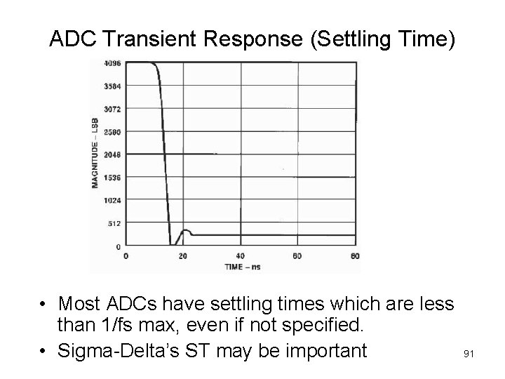
ADC Transient Response (Settling Time) • Most ADCs have settling times which are less than 1/fs max, even if not specified. • Sigma-Delta’s ST may be important 91

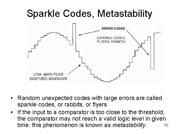
Sparkle Codes, Metastability • Random unexpected codes with large errors are called sparkle codes, or rabbits, or flyers • If the input to a comparator is too close to the threshold, the comparator may not reach a valid logic level in given 92 time: this phenomenon is known as metastability.

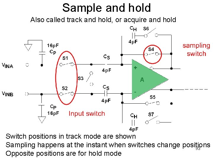
Sample and hold Also called track and hold, or acquire and hold Switch positions in track mode are shown Sampling happens at the instant when switches change positions 93 Opposite positions are for hold mode

Errors • During tracking – There is a voltage drop across op amp + and ─ terminal – There is voltage drop across S 1 and S 2 as long as Vin is not constant, i. e. , there is current – Both of the above cause Vcap ≠ Vin – Ron of S 1 and S 2 is also signal level dependent, making the above error non linear – This nonlinear error is also slope dependent, making it a dynamic error 94

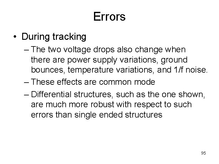
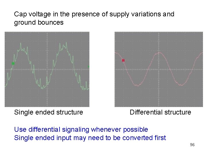
Errors • During tracking – The two voltage drops also change when there are power supply variations, ground bounces, temperature variations, and 1/f noise. – These effects are common mode – Differential structures, such as the one shown, are much more robust with respect to such errors than single ended structures 95

Cap voltage in the presence of supply variations and ground bounces Single ended structure Differential structure Use differential signaling whenever possible Single ended input may need to be converted first 96

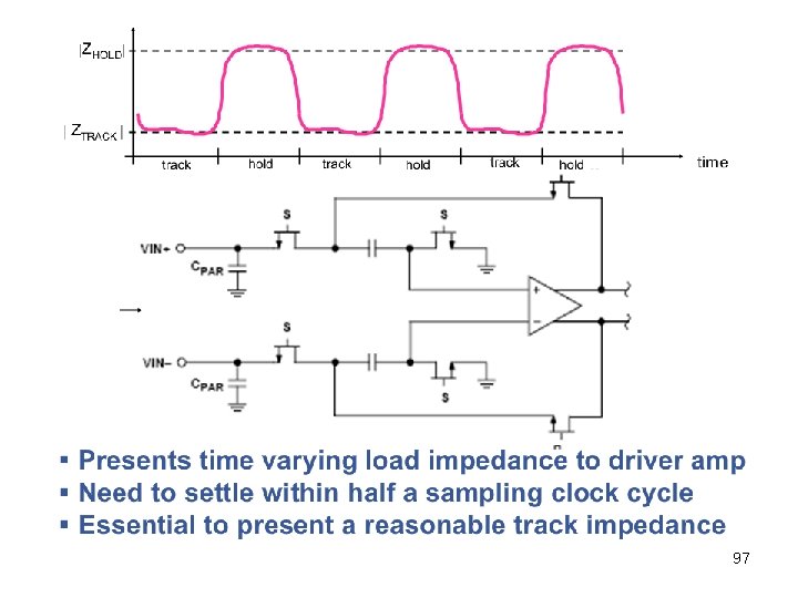
97

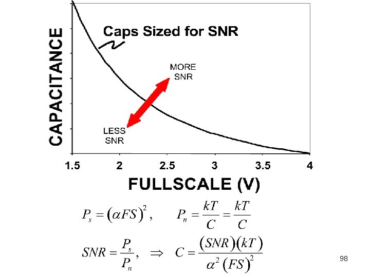
98

99

100

101

102