Lattice Semiconductor The Leader in ISP PLDs TM

- Slides: 15

Lattice Semiconductor The Leader in ISP PLDs TM Presents A Guide to JTAG Programming and Test © LATTICE SEMICONDUCTOR CORPORATION 2000 Uudet mikropiirit JTAG February 2001 1 Lattice Confidential

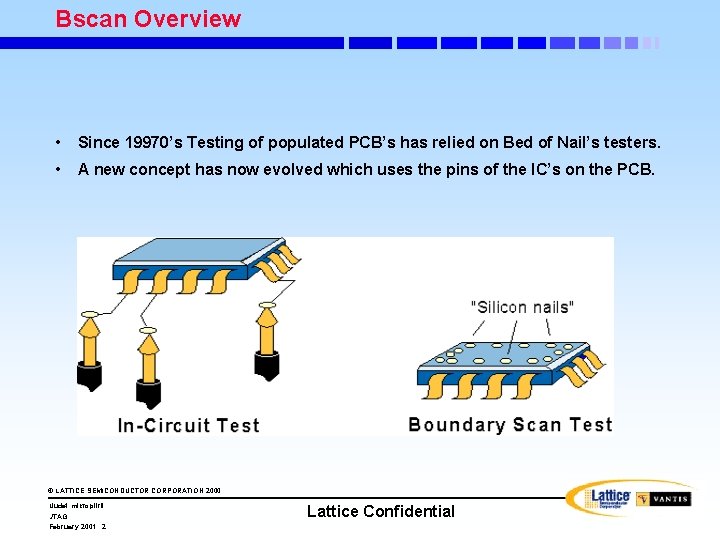
Bscan Overview • Since 19970’s Testing of populated PCB’s has relied on Bed of Nail’s testers. • A new concept has now evolved which uses the pins of the IC’s on the PCB. © LATTICE SEMICONDUCTOR CORPORATION 2000 Uudet mikropiirit JTAG February 2001 2 Lattice Confidential

Bscan Overview • Bed-of-nails testing involves accessing individual devices on the board through test lands laid into the copper interconnect, or other convenient contact points. • Testing of PCB’s using a Bed-of-nails can take the following form : • Power-off tests and Power-on tests. • Power-off tests check the integrity of the physical contact between nail and the on-board access point. Followed by open and shorts tests based on impedance measurements. • Power-on tests apply stimulus to a specific device on a board, which is accompanied by a measurement of the response from the device. • Devices which are not being tested are put into a safe state (All outputs Tri-Stated or isolated) in order to avoid signal contention. © LATTICE SEMICONDUCTOR CORPORATION 2000 Uudet mikropiirit JTAG February 2001 3 Lattice Confidential

Bscan Overview • Bed-of-nails testing has several major draw backs: • Physical space requirements on the PCB for the nail contacts. • Limit on the number of feasible connection points on the PCB. • Inability to test new surface mount packages ie: BGA as contact points for the all the required bed-of-nails points became impossible. • Each new PCB requires a new test fixture, which can involve a significant cost. • The ATE’s that perform the testing require significant capital expenditure. © LATTICE SEMICONDUCTOR CORPORATION 2000 Uudet mikropiirit JTAG February 2001 4 Lattice Confidential

Bscan Overview • In the mid-1980 s a group of concerned European test engineers sought a solution to the issues of PCB testing using the bed-ofnails technique. • The participants formed an organisation called Joint European Test Action Group (JETAG). • This organisations goal was to find a solution to PCB testing due to the draw backs from the existing bed-of-nails method. • The concept of a serial shift register around the boundary of the each individual device became the preferred solution. • This is where term “Boundary Scan” originated from. • After a period of time American companies joined the JETAG organisation, at this point in time the ‘E’ was dropped and it became the Joint Test Action Group (JTAG). • JTAG is the organisation responsible for creating the international standard. © LATTICE SEMICONDUCTOR CORPORATION 2000 Uudet mikropiirit JTAG February 2001 5 Lattice Confidential

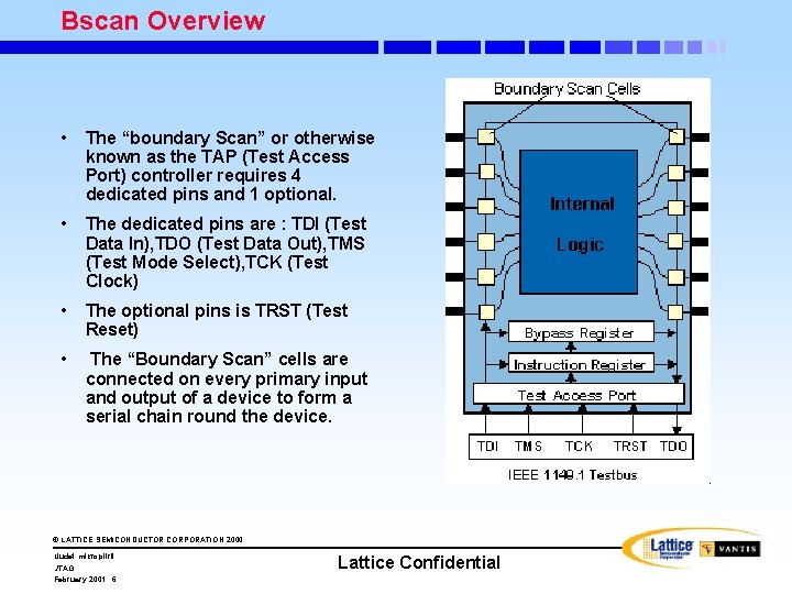
Bscan Overview • The “boundary Scan” or otherwise known as the TAP (Test Access Port) controller requires 4 dedicated pins and 1 optional. • The dedicated pins are : TDI (Test Data In), TDO (Test Data Out), TMS (Test Mode Select), TCK (Test Clock) • The optional pins is TRST (Test Reset) • The “Boundary Scan” cells are connected on every primary input and output of a device to form a serial chain round the device. © LATTICE SEMICONDUCTOR CORPORATION 2000 Uudet mikropiirit JTAG February 2001 6 Lattice Confidential

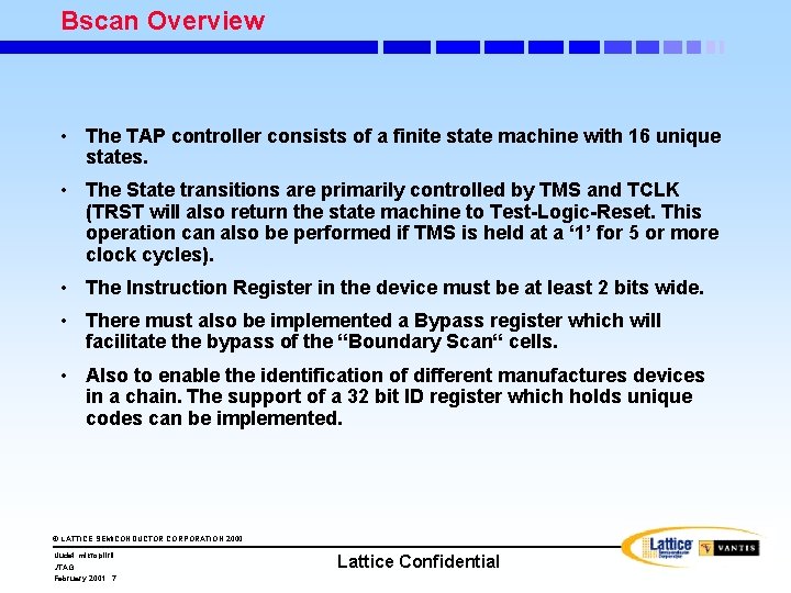
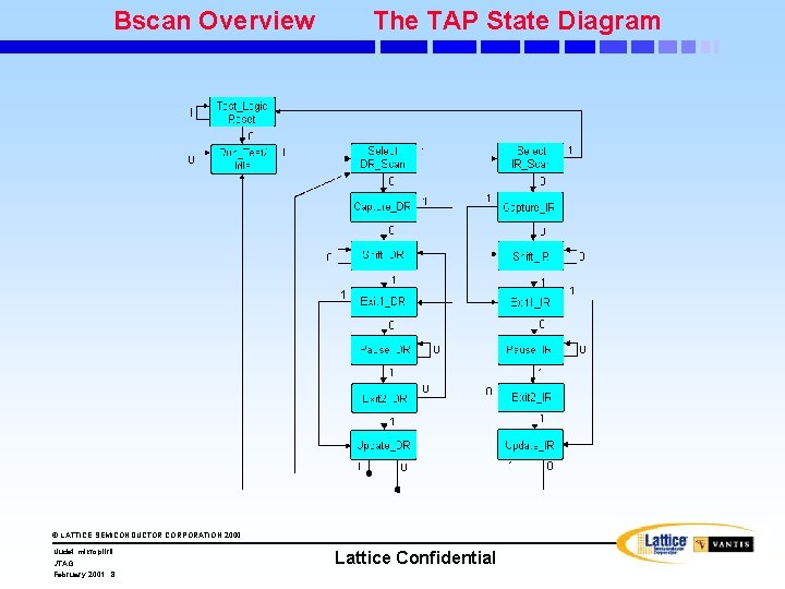
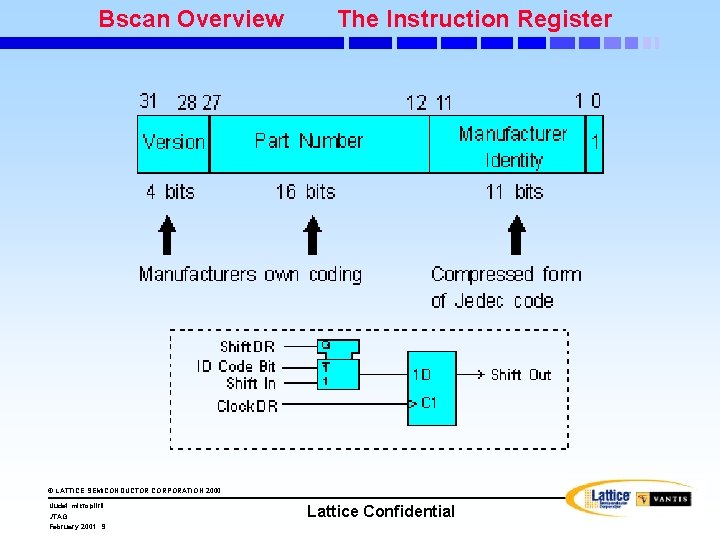
Bscan Overview • The TAP controller consists of a finite state machine with 16 unique states. • The State transitions are primarily controlled by TMS and TCLK (TRST will also return the state machine to Test-Logic-Reset. This operation can also be performed if TMS is held at a ‘ 1’ for 5 or more clock cycles). • The Instruction Register in the device must be at least 2 bits wide. • There must also be implemented a Bypass register which will facilitate the bypass of the “Boundary Scan“ cells. • Also to enable the identification of different manufactures devices in a chain. The support of a 32 bit ID register which holds unique codes can be implemented. © LATTICE SEMICONDUCTOR CORPORATION 2000 Uudet mikropiirit JTAG February 2001 7 Lattice Confidential

Bscan Overview The TAP State Diagram © LATTICE SEMICONDUCTOR CORPORATION 2000 Uudet mikropiirit JTAG February 2001 8 Lattice Confidential

Bscan Overview The Instruction Register © LATTICE SEMICONDUCTOR CORPORATION 2000 Uudet mikropiirit JTAG February 2001 9 Lattice Confidential

Bscan Overview • Only one of the possible internal registers can be connected from the TDI to TDO path. • The connection between TDI and TDO is controlled by the decoding of the instruction in the IR Register. • The JTAG specification provides for mandatory instructions ie: Extest, Bypass, Sample/Preload which must be supported by all silicon vendors. • The JTAG specification also provides for optional instructions ie : IDCODE. © LATTICE SEMICONDUCTOR CORPORATION 2000 Uudet mikropiirit JTAG February 2001 10 Lattice Confidential

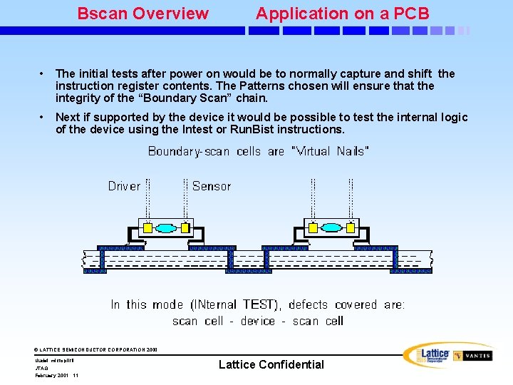
Bscan Overview Application on a PCB • The initial tests after power on would be to normally capture and shift the instruction register contents. The Patterns chosen will ensure that the integrity of the “Boundary Scan” chain. • Next if supported by the device it would be possible to test the internal logic of the device using the Intest or Run. Bist instructions. © LATTICE SEMICONDUCTOR CORPORATION 2000 Uudet mikropiirit JTAG February 2001 11 Lattice Confidential

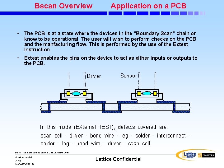
Bscan Overview Application on a PCB • The PCB is at a state where the devices in the “Boundary Scan” chain or know to be operational. The user will wish to perform checks on the PCB and the manfacturing flow. This is performed by the use of the Extest Instruction. • Extest enables the pins on the device to act as either inputs or outputs to the PCB. © LATTICE SEMICONDUCTOR CORPORATION 2000 Uudet mikropiirit JTAG February 2001 12 Lattice Confidential

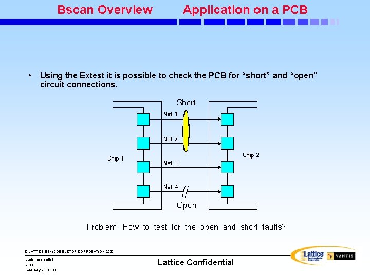
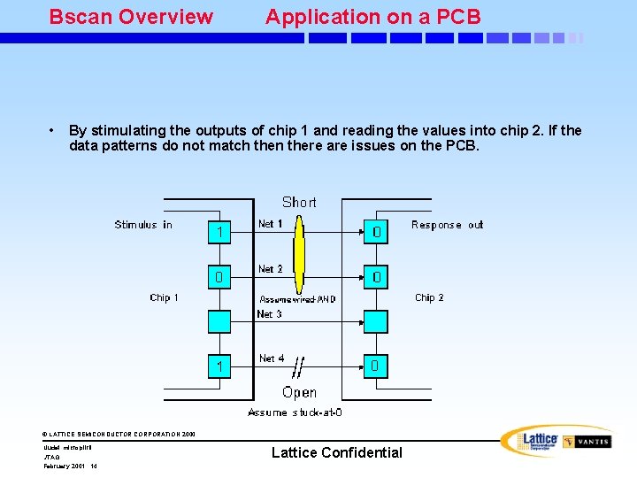
Bscan Overview • Application on a PCB Using the Extest it is possible to check the PCB for “short” and “open” circuit connections. © LATTICE SEMICONDUCTOR CORPORATION 2000 Uudet mikropiirit JTAG February 2001 13 Lattice Confidential

Bscan Overview • Application on a PCB By stimulating the outputs of chip 1 and reading the values into chip 2. If the data patterns do not match then there are issues on the PCB. © LATTICE SEMICONDUCTOR CORPORATION 2000 Uudet mikropiirit JTAG February 2001 14 Lattice Confidential

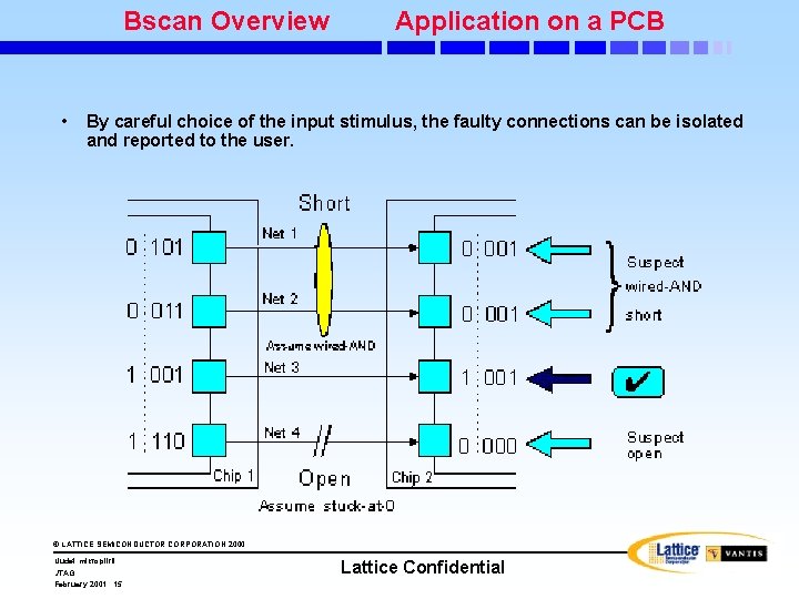
Bscan Overview • Application on a PCB By careful choice of the input stimulus, the faulty connections can be isolated and reported to the user. © LATTICE SEMICONDUCTOR CORPORATION 2000 Uudet mikropiirit JTAG February 2001 15 Lattice Confidential