Issues on Segmented LowGain Avalanche Detectors LGAD Hartmut
![Run 6827 LGAD Strips Pitch p=80 mm Strip w [mm] Metal [mm] P-implant [mm] Run 6827 LGAD Strips Pitch p=80 mm Strip w [mm] Metal [mm] P-implant [mm]](https://slidetodoc.com/presentation_image_h2/481a67ea01d45bf4bd0a6963e40d1972/image-4.jpg)
![Issues for 6827 Strip LGAD W 13 300 µm FZ Break-Down Voltage [V] 200 Issues for 6827 Strip LGAD W 13 300 µm FZ Break-Down Voltage [V] 200](https://slidetodoc.com/presentation_image_h2/481a67ea01d45bf4bd0a6963e40d1972/image-7.jpg)
![Doping Density Profile Device Voltage Lag [V] Nmax [cm-3] NBulk [cm-3] Gain (400 V) Doping Density Profile Device Voltage Lag [V] Nmax [cm-3] NBulk [cm-3] Gain (400 V)](https://slidetodoc.com/presentation_image_h2/481a67ea01d45bf4bd0a6963e40d1972/image-13.jpg)


- Slides: 31

Issues on Segmented Low-Gain Avalanche Detectors (LGAD) Hartmut F. W. Sadrozinski with Vitaliy Fadeyev, Patrick Freeman, Zachary Galloway, Zhijun Liang, Jeffrey Ngo, Colin Parker, Abe Seiden, Andriy Zatserklyaniy SCIPP, Univ. of California Santa Cruz Marta Baselga, Pablo Fernández-Martínez, Virginia Greco, Salvador Hidalgo, Giulio Pellegrini, David Quirion IMB-CNM-CSIC Nicolo Cartiglia, Francesca Cenna INFN Torino, Italy

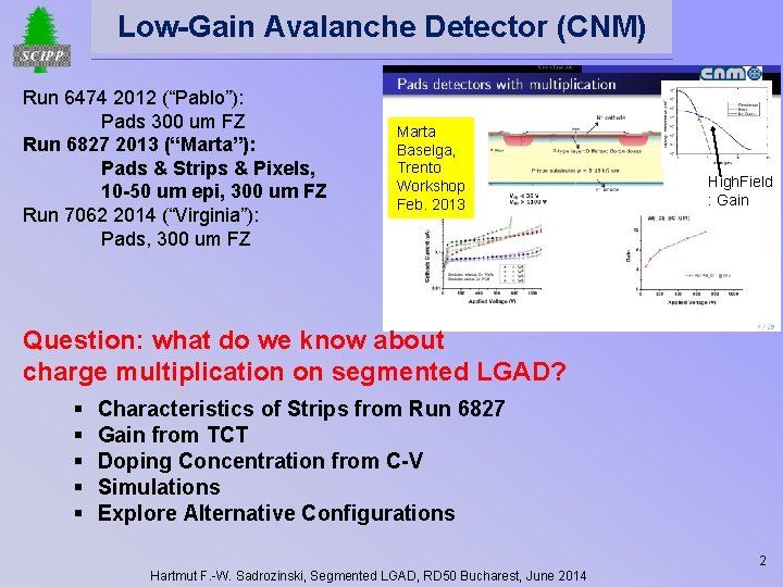
Low-Gain Avalanche Detector (CNM) Run 6474 2012 (“Pablo”): Pads 300 um FZ Run 6827 2013 (“Marta”): Pads & Strips & Pixels, 10 -50 um epi, 300 um FZ Run 7062 2014 (“Virginia”): Pads, 300 um FZ Marta Baselga, Trento Workshop Feb. 2013 High. Field : Gain Question: what do we know about charge multiplication on segmented LGAD? § § § Characteristics of Strips from Run 6827 Gain from TCT Doping Concentration from C-V Simulations Explore Alternative Configurations 2 Hartmut F. -W. Sadrozinski, Segmented LGAD, RD 50 Bucharest, June 2014

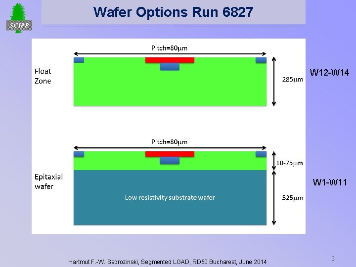
Wafer Options Run 6827 W 12 -W 14 W 1 -W 11 Hartmut F. -W. Sadrozinski, Segmented LGAD, RD 50 Bucharest, June 2014 3
![Run 6827 LGAD Strips Pitch p80 mm Strip w mm Metal mm Pimplant mm Run 6827 LGAD Strips Pitch p=80 mm Strip w [mm] Metal [mm] P-implant [mm]](https://slidetodoc.com/presentation_image_h2/481a67ea01d45bf4bd0a6963e40d1972/image-4.jpg)
Run 6827 LGAD Strips Pitch p=80 mm Strip w [mm] Metal [mm] P-implant [mm] w/p P-implant /pitch AC 1 24 20 6 0. 3 7. 5% AC 2 24 24 6 0. 3 7. 5% AC 3 24 28 6 0. 3 7. 5% AC 4 48 44 30 0. 6 37. 5% AC 5 48 48 30 0. 6 37. 5% AC 6 48 52 30 0. 6 37. 5% AC 7 62 58 44 0. 775 55% AC 8 62 62 44 0. 775 55% AC 9 62 66 44 0. 775 55% AC 10/AC 1 1/DC 32 40 14 0. 4 17. 5% In addition pixels, and pads with and without gain Hartmut F. -W. Sadrozinski, Segmented LGAD, RD 50 Bucharest, June 2014 4

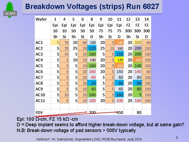
Breakdown Voltages (strips) Run 6827 Epi: 100 Ω-cm, FZ 15 kΩ -cm D = Deep implant seems to afford higher break-down voltage, but at same gain? N. B: Break-down voltage of pad sensors > 500 V typically Hartmut F. -W. Sadrozinski, Segmented LGAD, RD 50 Bucharest, June 2014 5

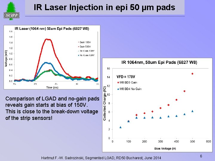
IR Laser Injection in epi 50 µm pads Comparison of LGAD and no-gain pads reveals gain starts at bias of 150 V. This is close to the break-down voltage of the strip sensors! Hartmut F. -W. Sadrozinski, Segmented LGAD, RD 50 Bucharest, June 2014 6
![Issues for 6827 Strip LGAD W 13 300 µm FZ BreakDown Voltage V 200 Issues for 6827 Strip LGAD W 13 300 µm FZ Break-Down Voltage [V] 200](https://slidetodoc.com/presentation_image_h2/481a67ea01d45bf4bd0a6963e40d1972/image-7.jpg)
Issues for 6827 Strip LGAD W 13 300 µm FZ Break-Down Voltage [V] 200 140 Issue of field at strip edge? 80 Uniformity of Response (p-layer covers between 7. 5% and 55% of pitch: what fraction of e- are traversing it and are multiplied? ) Simulations Charge collection Hartmut F. -W. Sadrozinski, Segmented LGAD, RD 50 Bucharest, June 2014 7

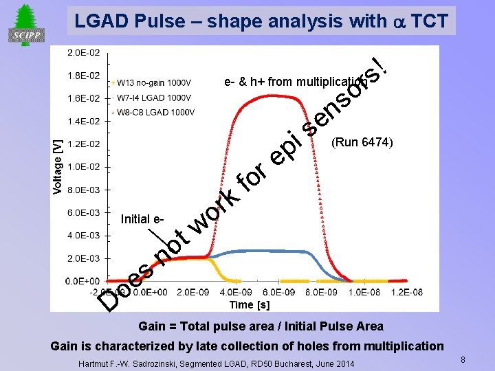
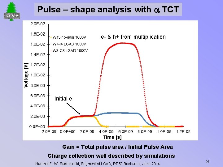
LGAD Pulse – shape analysis with TCT Initial e- s e o D n t o ! s e- & h+ from multiplicationr o s n e s (Run 6474) i p e r o f k r o w Gain = Total pulse area / Initial Pulse Area Gain is characterized by late collection of holes from multiplication Hartmut F. -W. Sadrozinski, Segmented LGAD, RD 50 Bucharest, June 2014 8

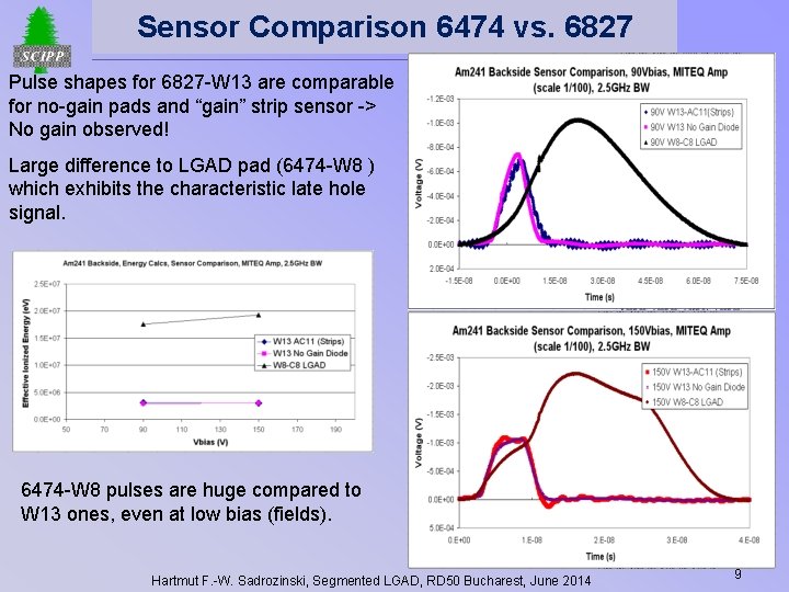
Sensor Comparison 6474 vs. 6827 Pulse shapes for 6827 -W 13 are comparable for no-gain pads and “gain” strip sensor -> No gain observed! Large difference to LGAD pad (6474 -W 8 ) which exhibits the characteristic late hole signal. 6474 -W 8 pulses are huge compared to W 13 ones, even at low bias (fields). Hartmut F. -W. Sadrozinski, Segmented LGAD, RD 50 Bucharest, June 2014 9

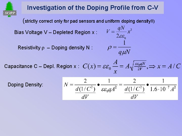
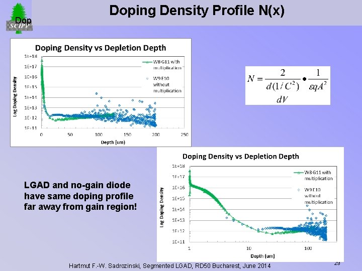
Investigation of the Doping Profile from C-V (strictly correct only for pad sensors and uniform doping density!!) Bias Voltage V – Depleted Region x : Resistivity r – Doping density N : Capacitance C – Depl. Region x : Doping Density:

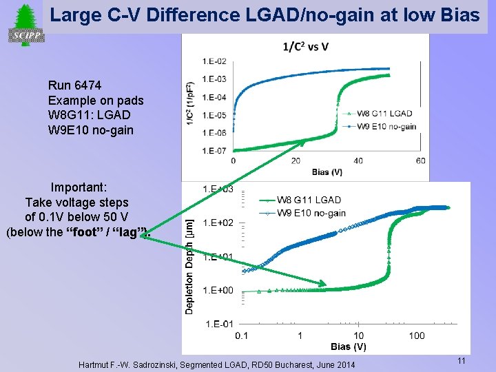
Large C-V Difference LGAD/no-gain at low Bias Run 6474 Example on pads W 8 G 11: LGAD W 9 E 10 no-gain Important: Take voltage steps of 0. 1 V below 50 V (below the “foot” / “lag”). Hartmut F. -W. Sadrozinski, Segmented LGAD, RD 50 Bucharest, June 2014 11

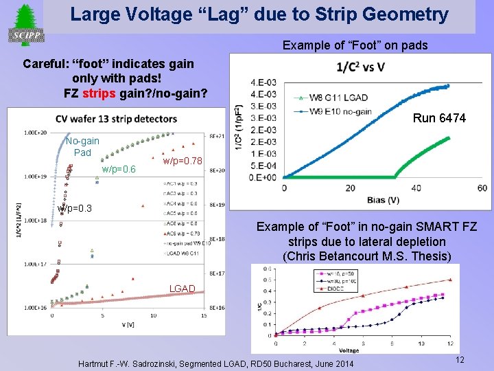
Large Voltage “Lag” due to Strip Geometry Example of “Foot” on pads Careful: “foot” indicates gain only with pads! FZ strips gain? /no-gain? Run 6474 No-gain Pad w/p=0. 6 w/p=0. 78 w/p=0. 3 Example of “Foot” in no-gain SMART FZ strips due to lateral depletion (Chris Betancourt M. S. Thesis) LGAD Hartmut F. -W. Sadrozinski, Segmented LGAD, RD 50 Bucharest, June 2014 12
![Doping Density Profile Device Voltage Lag V Nmax cm3 NBulk cm3 Gain 400 V Doping Density Profile Device Voltage Lag [V] Nmax [cm-3] NBulk [cm-3] Gain (400 V)](https://slidetodoc.com/presentation_image_h2/481a67ea01d45bf4bd0a6963e40d1972/image-13.jpg)
Doping Density Profile Device Voltage Lag [V] Nmax [cm-3] NBulk [cm-3] Gain (400 V) W 8 C 8 FZ (6474) 35 2. 0 e 16 1. 6 e 12 8 W 7 I 4 FZ (6474 29 1. 6 e 16 1. 6 e 12 2. 5 50 um epi (gain) 14 0. 6 e 16 7 e 13 ~ 1. 7 50 um epi (no-gain) <1 7 e 13 1 Hartmut F. -W. Sadrozinski, Segmented LGAD, RD 50 Bucharest, June 2014 13

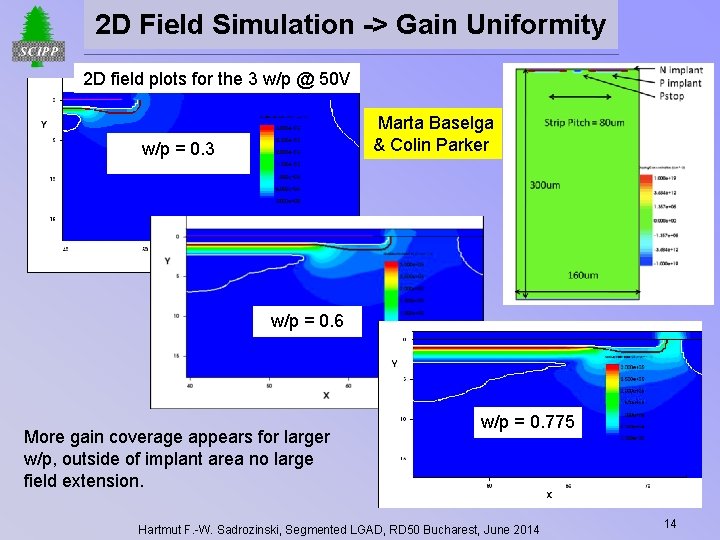
2 D Field Simulation -> Gain Uniformity 2 D field plots for the 3 w/p @ 50 V Marta Baselga & Colin Parker w/p = 0. 3 w/p = 0. 6 More gain coverage appears for larger w/p, outside of implant area no large field extension. w/p = 0. 775 Hartmut F. -W. Sadrozinski, Segmented LGAD, RD 50 Bucharest, June 2014 14

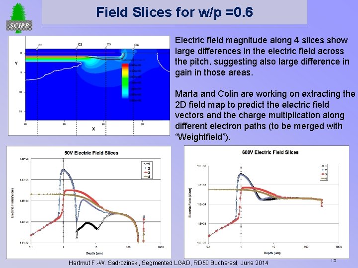
Field Slices for w/p =0. 6 Electric field magnitude along 4 slices show large differences in the electric field across the pitch, suggesting also large difference in gain in those areas. Marta and Colin are working on extracting the 2 D field map to predict the electric field vectors and the charge multiplication along different electron paths (to be merged with “Weightfield”). Hartmut F. -W. Sadrozinski, Segmented LGAD, RD 50 Bucharest, June 2014 15

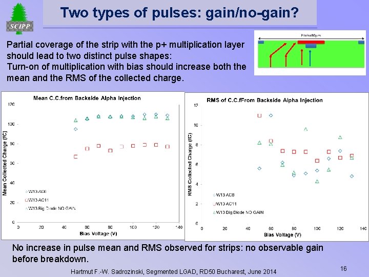
Two types of pulses: gain/no-gain? Partial coverage of the strip with the p+ multiplication layer should lead to two distinct pulse shapes: Turn-on of multiplication with bias should increase both the mean and the RMS of the collected charge. No increase in pulse mean and RMS observed for strips: no observable gain before breakdown. Hartmut F. -W. Sadrozinski, Segmented LGAD, RD 50 Bucharest, June 2014 16

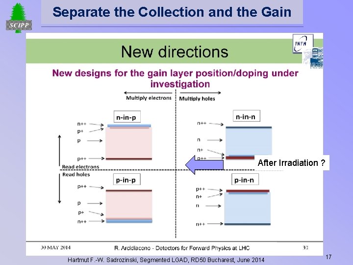
Separate the Collection and the Gain After Irradiation ? Hartmut F. -W. Sadrozinski, Segmented LGAD, RD 50 Bucharest, June 2014 17

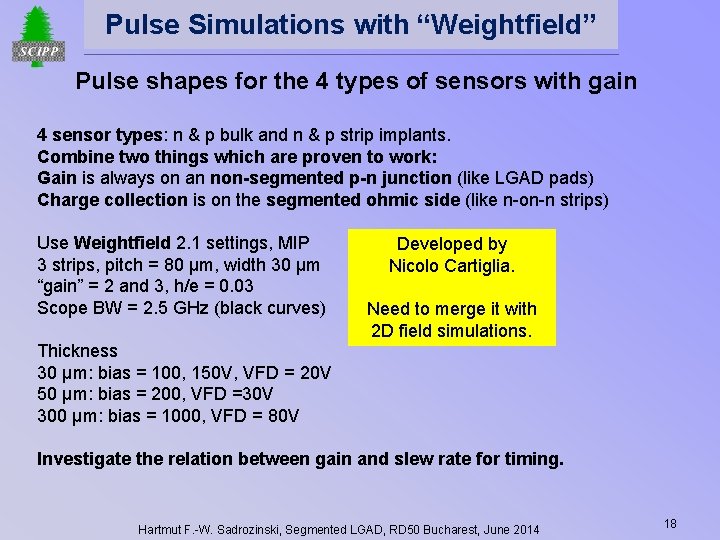
Pulse Simulations with “Weightfield” Pulse shapes for the 4 types of sensors with gain 4 sensor types: n & p bulk and n & p strip implants. Combine two things which are proven to work: Gain is always on an non-segmented p-n junction (like LGAD pads) Charge collection is on the segmented ohmic side (like n-on-n strips) Use Weightfield 2. 1 settings, MIP 3 strips, pitch = 80 µm, width 30 µm “gain” = 2 and 3, h/e = 0. 03 Scope BW = 2. 5 GHz (black curves) Developed by Nicolo Cartiglia. Need to merge it with 2 D field simulations. Thickness 30 µm: bias = 100, 150 V, VFD = 20 V 50 µm: bias = 200, VFD =30 V 300 µm: bias = 1000, VFD = 80 V Investigate the relation between gain and slew rate for timing. Hartmut F. -W. Sadrozinski, Segmented LGAD, RD 50 Bucharest, June 2014 18

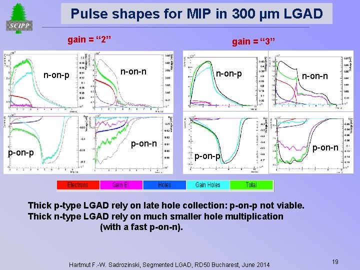
Pulse shapes for MIP in 300 µm LGAD gain = “ 2” n-on-p p-on-p gain = “ 3” n-on-n n-on-p n-on-n p-on-p p-on-n Thick p-type LGAD rely on late hole collection: p-on-p not viable. Thick n-type LGAD rely on much smaller hole multiplication (with a fast p-on-n). Hartmut F. -W. Sadrozinski, Segmented LGAD, RD 50 Bucharest, June 2014 19

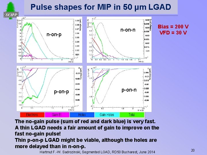
Pulse shapes for MIP in 50 µm LGAD n-on-p p-on-p n-on-n Bias = 200 V VFD = 30 V p-on-n The no-gain pulse (sum of red and dark blue) is very fast. A thin LGAD needs a fair amount of gain to improve on the fast no-gain pulse! Thin p-on-p LGAD might be viable, although the holes are more delayed than in n-on-p. Hartmut F. -W. Sadrozinski, Segmented LGAD, RD 50 Bucharest, June 2014 20

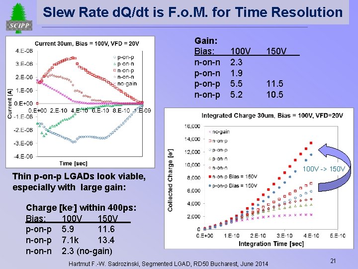
Slew Rate d. Q/dt is F. o. M. for Time Resolution Gain: Bias: n-on-n p-on-p n-on-p 100 V 2. 3 1. 9 5. 5 5. 2 150 V 11. 5 10. 5 Thin p-on-p LGADs look viable, especially with large gain: 100 V -> 150 V Charge [ke-] within 400 ps: Bias: 100 V 150 V p-on-p 5. 9 11. 6 n-on-p 7. 1 k 13. 4 n-on-n 2. 3 (no-gain) Hartmut F. -W. Sadrozinski, Segmented LGAD, RD 50 Bucharest, June 2014 21

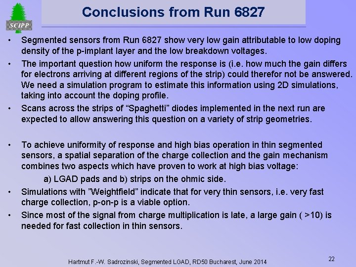
Conclusions from Run 6827 Conclusions • • • Segmented sensors from Run 6827 show very low gain attributable to low doping density of the p-implant layer and the low breakdown voltages. The important question how uniform the response is (i. e. how much the gain differs for electrons arriving at different regions of the strip) could therefor not be answered. We need a simulation program to estimate this information using 2 D simulations, taking into account the doping profile. Scans across the strips of “Spaghetti” diodes implemented in the next run are expected to allow answering this question on a variety of strip geometries. To achieve uniformity of response and high bias operation in thin segmented sensors, a spatial separation of the charge collection and the gain mechanism combines two aspects which have proven to work at high bias voltage: a) LGAD pads and b) strips on the ohmic side. Simulations with ”Weightfield” indicate that for very thin sensors, i. e. very fast charge collection, p-on-p is a viable option. Since most of the signal from charge multiplication is late, a large gain ( >10) is needed for fast collection in thin sensors. Hartmut F. -W. Sadrozinski, Segmented LGAD, RD 50 Bucharest, June 2014 22

Acknowledgements Conclusions Part of this work has been performed in the framework of the CERN RD-50 collaboration and (partially) financed by the Spanish Ministry of Education and Science through the Particle Physics National Program (FPA 2010 -22060 -C 0202 and FPA 2010 -22163_C 02 -02). Marta Baselga acknowledges a stipend from the Spanish Ministry of Science and Innovation (FPA 2010 -22060 -C 02 -02). This research was carried out with the contribution of the Ministero degli Affari Esteri, “Direzione Generale per la Promozione del Sistema Paese” of Italy. The work at SCIPP was partially supported by the United States Department of Energy, grant DE-FG 02 -04 ER 41286. Hartmut F. -W. Sadrozinski, Segmented LGAD, RD 50 Bucharest, June 2014 23

Back-up Hartmut F. -W. Sadrozinski, Segmented LGAD, RD 50 Bucharest, June 2014 24

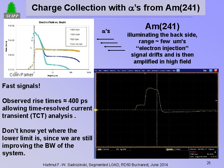
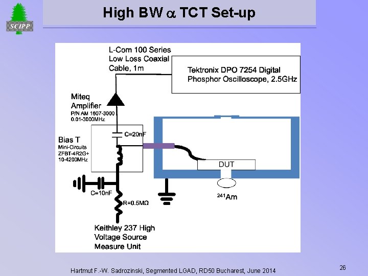
Charge Collection with ’s from Am(241) ’s Am(241) illuminating the back side, range ~ few um’s “electron injection” signal drifts and is then amplified in high field Colin Parker Fast signals! Observed rise times ≈ 400 ps allowing time-resolved current transient (TCT) analysis. Don’t know yet where the lower limit is, since we are still improving the BW of the system. Hartmut F. -W. Sadrozinski, Segmented LGAD, RD 50 Bucharest, June 2014 25

High BW TCT Set-up Hartmut F. -W. Sadrozinski, Segmented LGAD, RD 50 Bucharest, June 2014 26

Pulse – shape analysis with TCT e- & h+ from multiplication Initial e- Gain = Total pulse area / Initial Pulse Area Charge collection well described by simulations Hartmut F. -W. Sadrozinski, Segmented LGAD, RD 50 Bucharest, June 2014 27

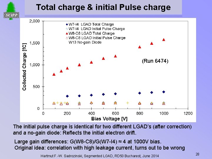
Total charge & initial Pulse charge (Run 6474) The initial pulse charge is identical for two different LGAD’s (after correction) and a no-gain diode: Reflects the initial electron drift. Large gain differences: G(W 8 -C 8)/G(W 7 -I 4) ≈ 4 at 1000 V bias. Original idea: correlation with high leakage current, turns out to be wrong Hartmut F. -W. Sadrozinski, Segmented LGAD, RD 50 Bucharest, June 2014 28

Doping density N(x) Doping Density Profile N(x) LGAD and no-gain diode have same doping profile far away from gain region! Hartmut F. -W. Sadrozinski, Segmented LGAD, RD 50 Bucharest, June 2014 29

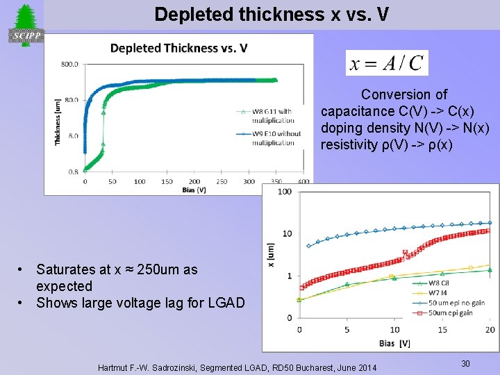
Depleted thickness x vs. V Conversion of capacitance C(V) -> C(x) doping density N(V) -> N(x) resistivity ρ(V) -> ρ(x) • Saturates at x ≈ 250 um as expected • Shows large voltage lag for LGAD Hartmut F. -W. Sadrozinski, Segmented LGAD, RD 50 Bucharest, June 2014 30

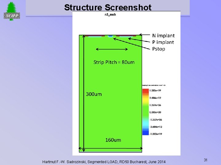
Structure Screenshot Hartmut F. -W. Sadrozinski, Segmented LGAD, RD 50 Bucharest, June 2014 31