Experience with 50 um thick epi LGAD Hartmut
![Doping Density Profile (C-V) Device 6474 W 8 C 8 FZ Voltage Lag [V] Doping Density Profile (C-V) Device 6474 W 8 C 8 FZ Voltage Lag [V]](https://slidetodoc.com/presentation_image/11e55eb17e50a3b6d935759b13e968b6/image-11.jpg)
- Slides: 17

Experience with 50 um thick epi LGAD Hartmut F. W. Sadrozinski with Caitlin Celic, Scott Ely, Vitaliy Fadeyev, Patrick Freeman, Zachary Galloway, Zhijun Liang, Colin Parker, Abe Seiden, Andriy Zatserklyaniy SCIPP, Univ. of California Santa Cruz, USA Marta Baselga, Pablo Fernández-Martínez, David Flores , Virginia Greco, Salvador Hidalgo, Giulio Pellegrini, David Quirion, IMB-CNM, Barcelona, Spain Nicolo Cartiglia, Francesca Cenna INFN Torino, Italy Why LGAD, why thin? CCE (IR Laser, top ) Gain thin-thick Doping Profile Hartmut F. -W. Sadrozinski, thin LGAD, 25 th RD 50, Nov 2014

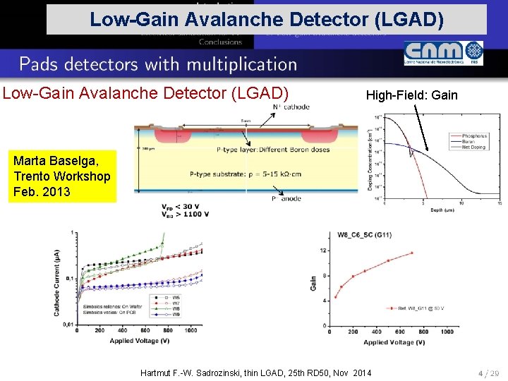
Low-Gain Avalanche Detector (LGAD) High-Field: Gain Marta Baselga, Trento Workshop Feb. 2013 Hartmut F. -W. Sadrozinski, thin LGAD, 25 th RD 50, Nov 2014

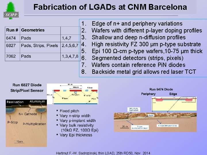
Fabrication of LGADs at CNM Barcelona 1. 2. 3. 4. 5. 6. 7. 8. Edge of n+ and periphery variations Wafers with different p-layer doping profiles Shallow and deep n-diffusion profiles High resistivity FZ 300 μm p-type substrate Epi 100 Ω-cm p-type wafers, 10 -75 µm thick Segmented detectors (strips, pixels) Wafers contain reference Pi. N diodes Backside metal grid allows red laser TCT Hartmut F. -W. Sadrozinski, thin LGAD, 25 th RD 50, Nov 2014

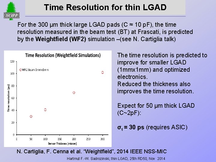
Time Resolution for thin LGAD For the 300 µm thick large LGAD pads (C ≈ 10 p. F), the time resolution measured in the beam test (BT) at Frascati, is predicted by the Weightfield (WF 2) simulation –(see N. Cartiglia talk) The time resolution is predicted to improve for smaller LGAD (1 mmx 1 mm) and optimized electronics. Reduced the thickness also improves the time resolution. Expect for 50 µm thick LGAD (C~2 p. F): σt = 30 ps (requires ASIC) N. Cartiglia, F. Cenna et al. “Weightfield”, 2014 IEEE NSS-MIC Hartmut F. -W. Sadrozinski, thin LGAD, 25 th RD 50, Nov 2014

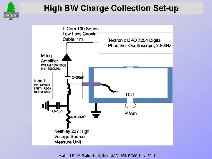
High BW Charge Collection Set-up Hartmut F. -W. Sadrozinski, thin LGAD, 25 th RD 50, Nov 2014

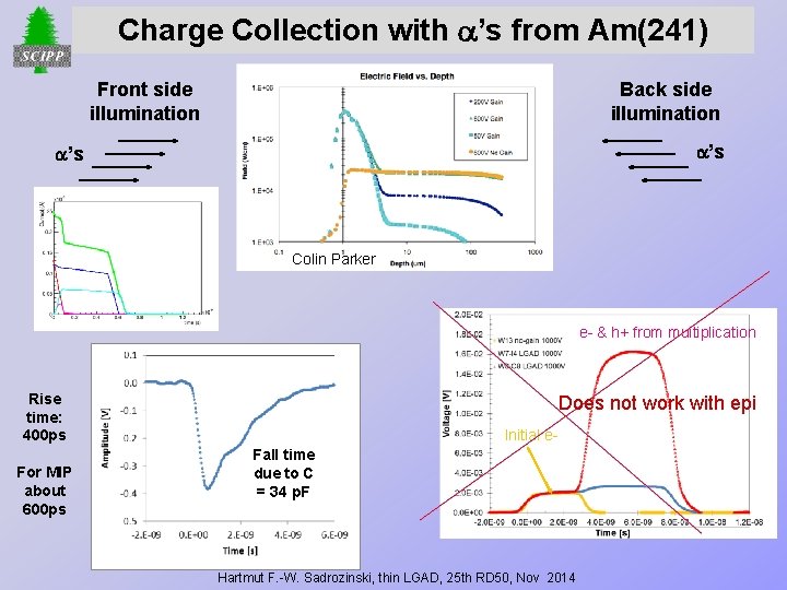
Charge Collection with ’s from Am(241) Front side illumination Back side illumination ’s Colin Parker e- & h+ from multiplication Rise time: 400 ps For MIP about 600 ps Does not work with epi Initial e. Fall time due to C = 34 p. F Hartmut F. -W. Sadrozinski, thin LGAD, 25 th RD 50, Nov 2014

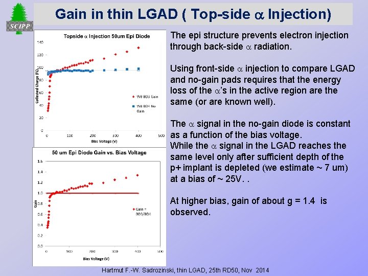
Gain in thin LGAD ( Top-side Injection) The epi structure prevents electron injection through back-side radiation. Using front-side injection to compare LGAD and no-gain pads requires that the energy loss of the ’s in the active region are the same (or are known well). The signal in the no-gain diode is constant as a function of the bias voltage. While the signal in the LGAD reaches the same level only after sufficient depth of the p+ implant is depleted (we estimate ~ 7 um) at a bias of ~ 25 V. . At higher bias, gain of about g = 1. 4 is observed. Hartmut F. -W. Sadrozinski, thin LGAD, 25 th RD 50, Nov 2014

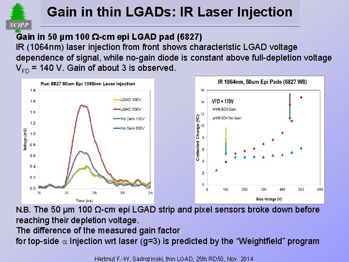
Gain in thin LGADs: IR Laser Injection Gain in 50 µm 100 Ω-cm epi LGAD pad (6827) IR (1064 nm) laser injection from front shows characteristic LGAD voltage dependence of signal, while no-gain diode is constant above full-depletion voltage VFD = 140 V. Gain of about 3 is observed. N. B. The 50 µm 100 Ω-cm epi LGAD strip and pixel sensors broke down before reaching their depletion voltage. The difference of the measured gain factor for top-side Injection wrt laser (g=3) is predicted by the “Weightfield” program Hartmut F. -W. Sadrozinski, thin LGAD, 25 th RD 50, Nov 2014

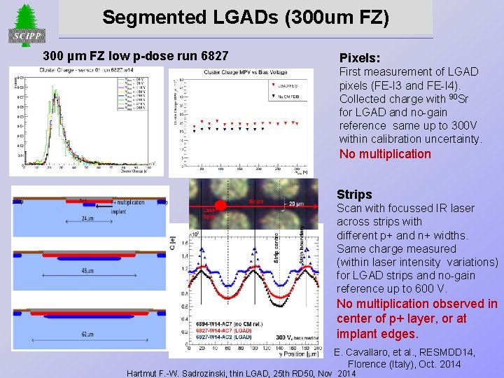
Segmented LGADs (300 um FZ) 300 µm FZ low p-dose run 6827 Pixels: First measurement of LGAD pixels (FE-I 3 and FE-I 4). Collected charge with 90 Sr for LGAD and no-gain reference same up to 300 V within calibration uncertainty. No multiplication Strips Scan with focussed IR laser across strips with different p+ and n+ widths. Same charge measured (within laser intensity variations) for LGAD strips and no-gain reference up to 600 V. No multiplication observed in center of p+ layer, or at implant edges. E. Cavallaro, et al. , RESMDD 14, Florence (Italy), Oct. 2014 Hartmut F. -W. Sadrozinski, thin LGAD, 25 th RD 50, Nov 2014

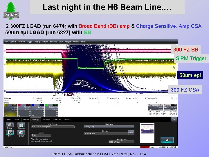
Last night in the H 6 Beam Line…. 2 300 FZ LGAD (run 6474) with Broad Band (BB) amp & Charge Sensitive. Amp CSA 50 um epi LGAD (run 6827) with BB 300 FZ BB Si. PM Trigger 50 um epi 300 FZ CSA Hartmut F. -W. Sadrozinski, thin LGAD, 25 th RD 50, Nov 2014
![Doping Density Profile CV Device 6474 W 8 C 8 FZ Voltage Lag V Doping Density Profile (C-V) Device 6474 W 8 C 8 FZ Voltage Lag [V]](https://slidetodoc.com/presentation_image/11e55eb17e50a3b6d935759b13e968b6/image-11.jpg)
Doping Density Profile (C-V) Device 6474 W 8 C 8 FZ Voltage Lag [V] Nmax [cm-3] 35 1. 2 e 16 NBulk [cm-3] 1 e 12 Gain (400 V) 8 6474 W 7 I 4 FZ 29 1. 0 e 16 1. e 12 2. 5 6827 W 13 300 um FZ 14 0. 8 e 16 1. e 12 1 6827 W 8 50 um epi (gain) 14 0. 8 e 16 1. 1 e 14 1. 4 -2 6827 W 8 50 um epi (no-gain) <1 7 e 13 1. 1 e 14 1 Hartmut F. -W. Sadrozinski, thin LGAD, 25 th RD 50, Nov 2014

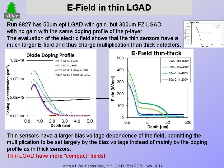
E-Field in thin LGAD Run 6827 has 50 um epi LGAD with gain, but 300 um FZ LGAD with no gain with the same doping profile of the p-layer. The evaluation of the electric field shows that the thin sensors have a much larger E-field and thus charge multiplication than thick detectors. E-Field thin-thick Thin sensors have a larger bias voltage dependence of the field, permitting the multiplication to be set largely by the bias voltage instead of mainly by the doping profile as in thick sensors. Thin LGAD have more “compact” fields! Hartmut F. -W. Sadrozinski, thin LGAD, 25 th RD 50, Nov 2014

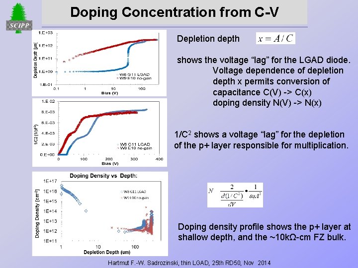
Doping Concentration from C-V Depletion depth shows the voltage “lag” for the LGAD diode. Voltage dependence of depletion depth x permits conversion of capacitance C(V) -> C(x) doping density N(V) -> N(x) 1/C 2 shows a voltage “lag” for the depletion of the p+ layer responsible for multiplication. Doping density profile shows the p+ layer at shallow depth, and the ~10 kΩ-cm FZ bulk. Hartmut F. -W. Sadrozinski, thin LGAD, 25 th RD 50, Nov 2014

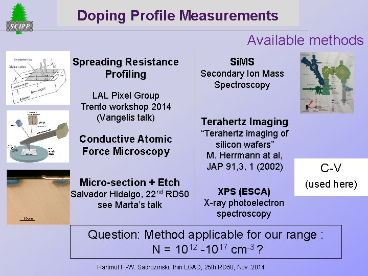
Doping Profile Measurements Available methods Spreading Resistance Profiling LAL Pixel Group Trento workshop 2014 (Vangelis talk) Conductive Atomic Force Microscopy Micro-section + Etch Salvador Hidalgo, 22 nd RD 50 see Marta’s talk Si. MS Secondary Ion Mass Spectroscopy Terahertz Imaging “Terahertz imaging of silicon wafers” M. Herrmann at al, JAP 91, 3, 1 (2002) XPS (ESCA) X-ray photoelectron spectroscopy C-V (used here) Question: Method applicable for our range : N = 1012 -1017 cm-3 ? Hartmut F. -W. Sadrozinski, thin LGAD, 25 th RD 50, Nov 2014

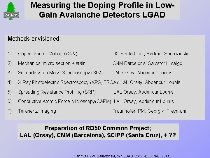
Measuring the Doping Profile in Low. Gain Avalanche Detectors LGAD Methods envisioned: 1) Capacitance – Voltage (C-V): UC Santa Cruz, Hartmut Sadrozinski 2) Mechanical micro-section + stain: CNM Barcelona, Salvator Hidalgo 3) Secondary Ion Mass Spectroscopy (SIM): : LAL Orsay, Abdenour Lounis 4) X-Ray Photoelectric Spectroscopy (XPS, ESCA): LAL Orsay, Abdenour Lounis 5) Spreading Resistance Profiling (SRP): 6) Conductive Atomic Force Microscopy(CAFM): LAL Orsay, Abdenour Lounis 7) Terahertz Imaging: LAL Orsay, Abdenour Lounis Fraunhofer IPM, Georg v. Freymann Preparation of RD 50 Common Project; LAL (Orsay), CNM (Barcelona), SCIPP (Santa Cruz), + ? ? Hartmut F. -W. Sadrozinski, thin LGAD, 25 th RD 50, Nov 2014

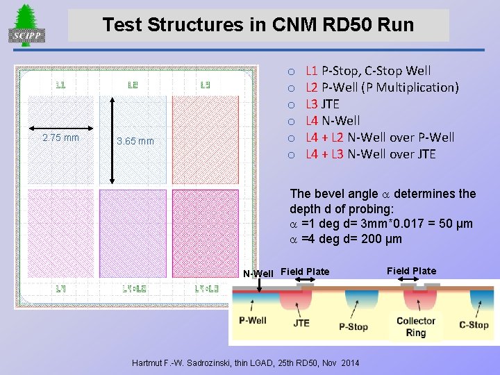
Test Structures in CNM RD 50 Run 2. 75 mm 3. 65 mm o o o L 1 P-Stop, C-Stop Well L 2 P-Well (P Multiplication) L 3 JTE L 4 N-Well L 4 + L 2 N-Well over P-Well L 4 + L 3 N-Well over JTE The bevel angle determines the depth d of probing: =1 deg d= 3 mm*0. 017 = 50 µm =4 deg d= 200 µm N-Well Field Plate Hartmut F. -W. Sadrozinski, thin LGAD, 25 th RD 50, Nov 2014 Field Plate

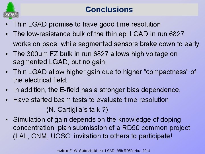
Conclusions • Thin LGAD promise to have good time resolution • The low-resistance bulk of the thin epi LGAD in run 6827 works on pads, while segmented sensors brake down to early. • The 300 um FZ bulk in run 6827 allows high voltage on segmented LGAD, but no gain. • Thin LGAD allow higher gain due to higher “compactness” of the electrical field. • In addition, the E-field has a stronger bias dependence. • Have started beam tests to evaluate time resolution (N. Cartiglia’s talk ? ) • Simulation of gain depends on the knowledge of doping concentration: plan submission of a RD 50 common project (LAL, CNM, UCSC: invitation to others to participate! Hartmut F. -W. Sadrozinski, thin LGAD, 25 th RD 50, Nov 2014