Integrated Photonics Figures and Images for Instructors Module

- Slides: 28

Integrated Photonics Figures and Images for Instructors Module 3 III-V Semiconductor Devices Optics and Photonics Series

© 2018 University of Central Florida This text was developed by the National Center for Optics and Photonics Education (OP-TEC), University of Central Florida, under NSF ATE grant 1303732. Any opinions, findings, and conclusions or recommendations expressed in this material are those of the author(s) and do not necessarily reflect the views of the National Science Foundation. Published and distributed by OP-TEC University of Central Florida http: //www. op-tec. org Permission to copy and distribute This work is licensed under the Creative Commons Attribution-Non. Commercial-No. Derivatives 4. 0 International License. http: //creativecommons. org/licenses/by-nc-nd/4. 0. Individuals and organizations may copy and distribute this material for non-commercial purposes. Appropriate credit to the University of Central Florida & the National Science Foundation shall be displayed, by retaining the statements on this page. 2

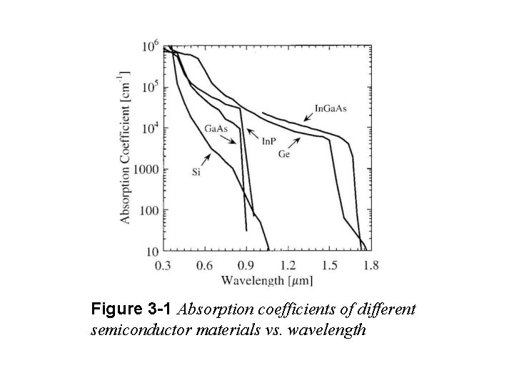
Figure 3 -1 Absorption coefficients of different semiconductor materials vs. wavelength

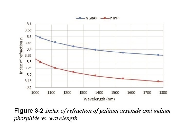
Figure 3 -2 Index of refraction of gallium arsenide and indium phosphide vs. wavelength

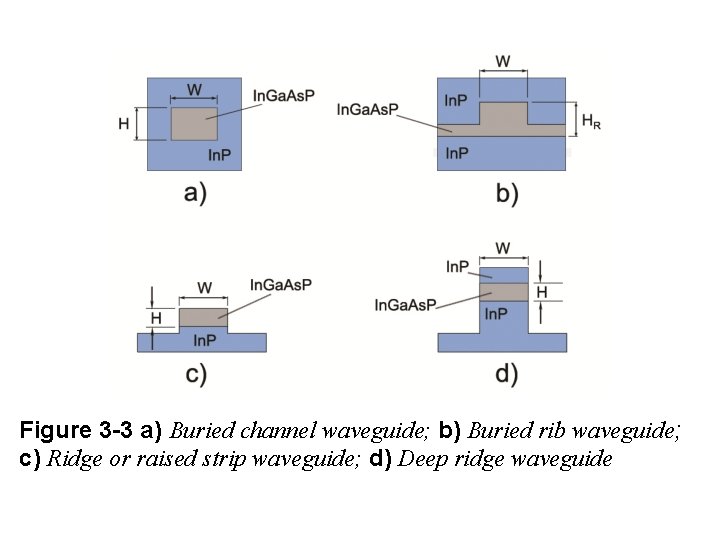
Figure 3 -3 a) Buried channel waveguide; b) Buried rib waveguide; c) Ridge or raised strip waveguide; d) Deep ridge waveguide

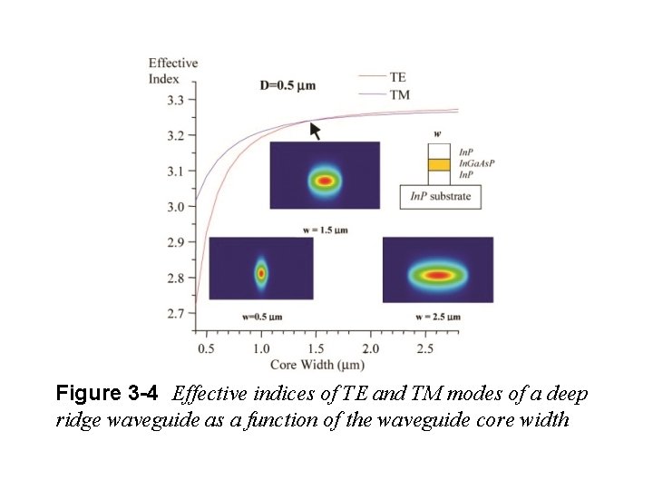
Figure 3 -4 Effective indices of TE and TM modes of a deep ridge waveguide as a function of the waveguide core width

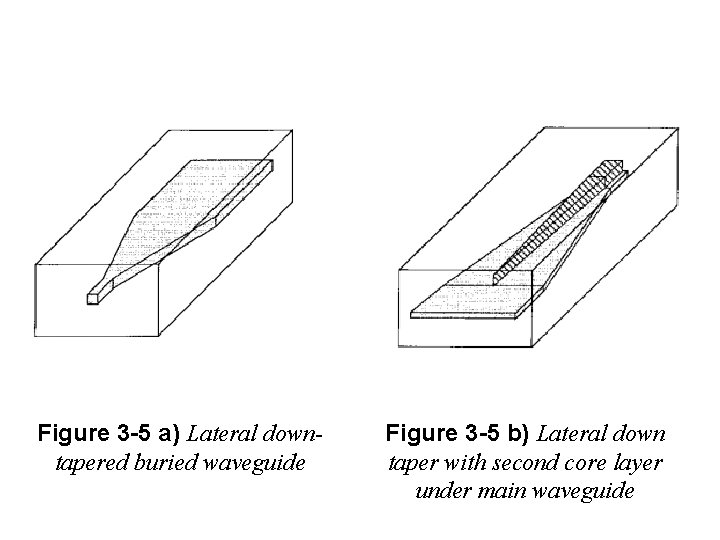
Figure 3 -5 a) Lateral downtapered buried waveguide Figure 3 -5 b) Lateral down taper with second core layer under main waveguide

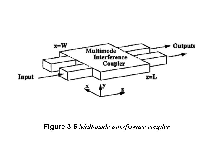
Figure 3 -6 Multimode interference coupler

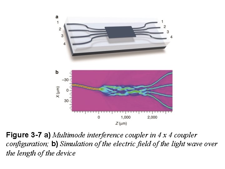
Figure 3 -7 a) Multimode interference coupler in 4 x 4 coupler configuration; b) Simulation of the electric field of the light wave over the length of the device

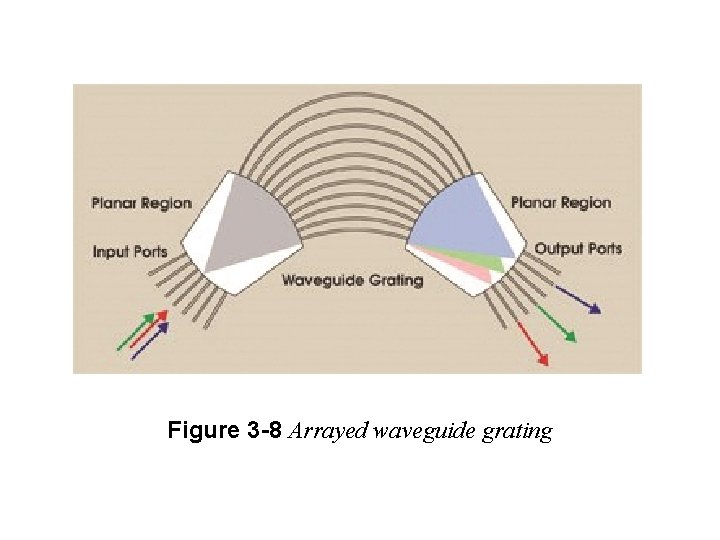
Figure 3 -8 Arrayed waveguide grating

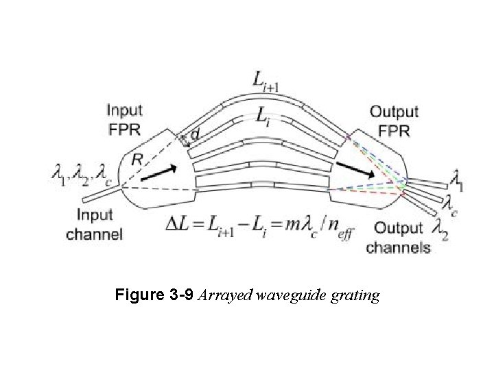
Figure 3 -9 Arrayed waveguide grating

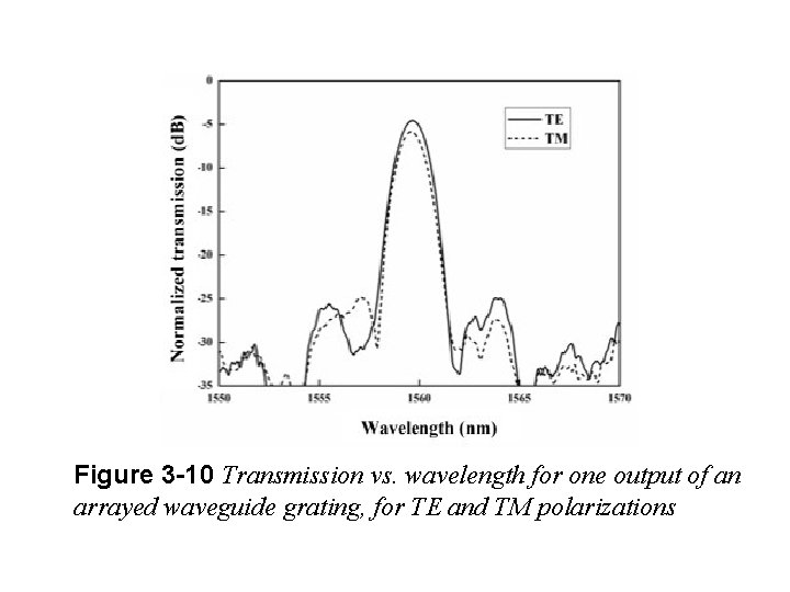
Figure 3 -10 Transmission vs. wavelength for one output of an arrayed waveguide grating, for TE and TM polarizations

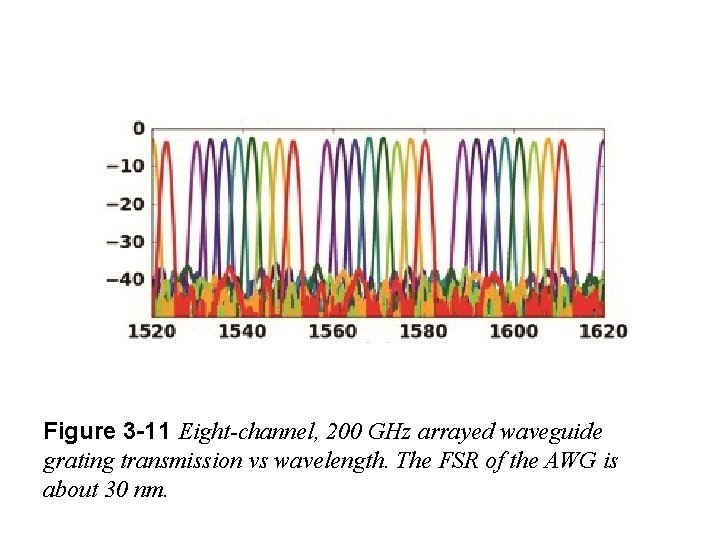
Figure 3 -11 Eight-channel, 200 GHz arrayed waveguide grating transmission vs wavelength. The FSR of the AWG is about 30 nm.

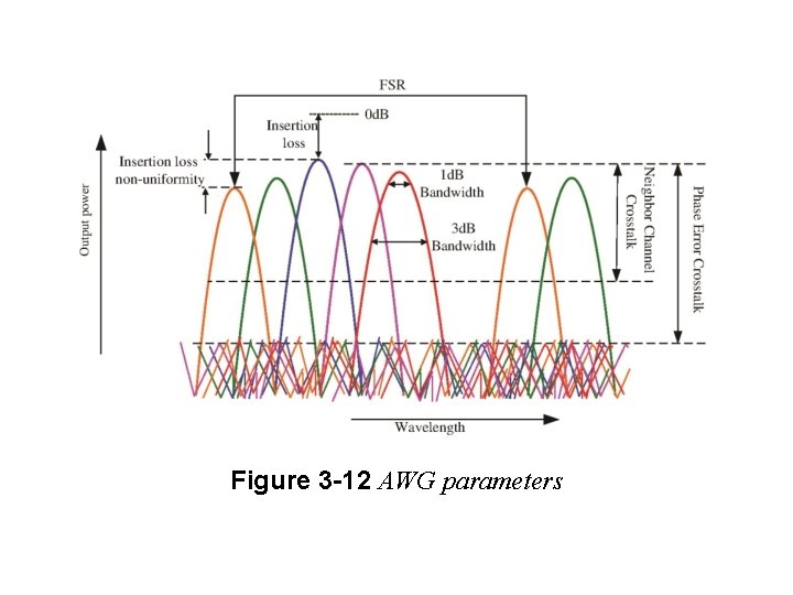
Figure 3 -12 AWG parameters

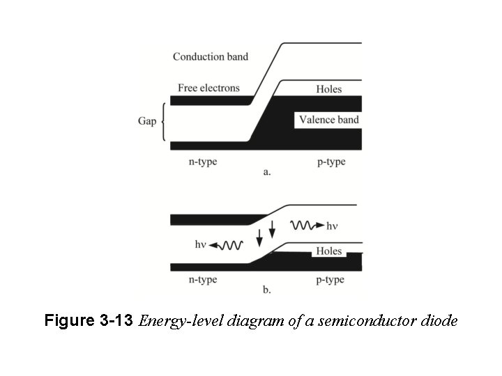
Figure 3 -13 Energy-level diagram of a semiconductor diode

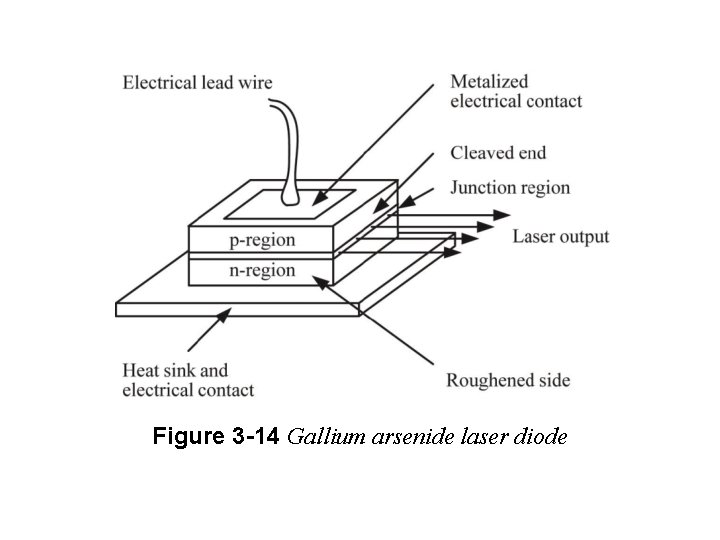
Figure 3 -14 Gallium arsenide laser diode

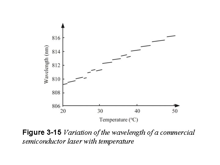
Figure 3 -15 Variation of the wavelength of a commercial semiconductor laser with temperature

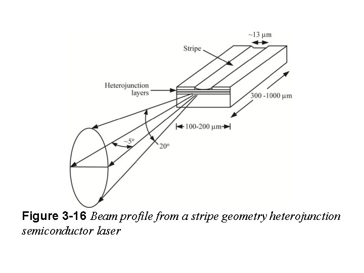
Figure 3 -16 Beam profile from a stripe geometry heterojunction semiconductor laser

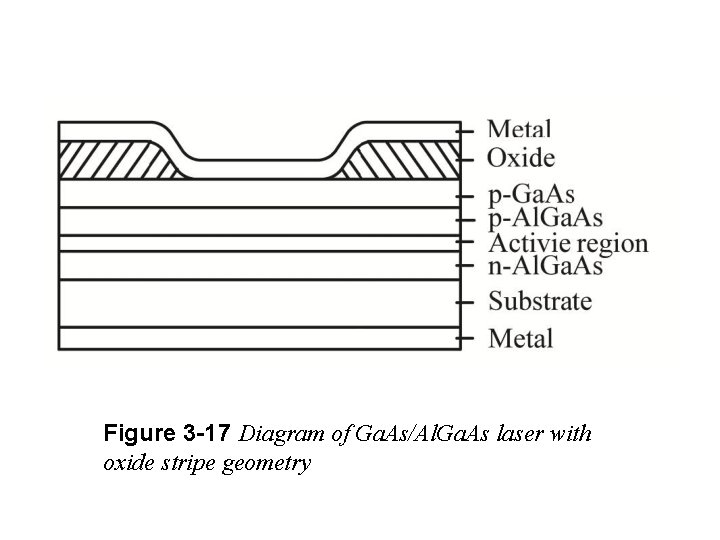
Figure 3 -17 Diagram of Ga. As/Al. Ga. As laser with oxide stripe geometry

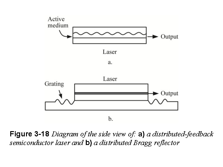
Figure 3 -18 Diagram of the side view of: a) a distributed-feedback semiconductor laser and b) a distributed Bragg reflector

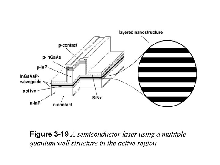
Figure 3 -19 A semiconductor laser using a multiple quantum well structure in the active region

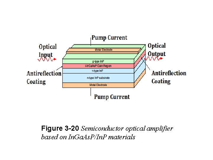
Figure 3 -20 Semiconductor optical amplifier based on In. Ga. As. P/In. P materials

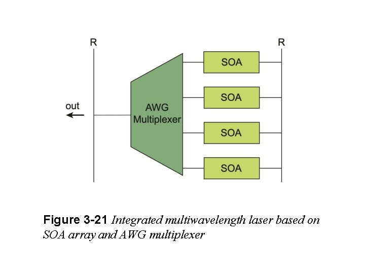
Figure 3 -21 Integrated multiwavelength laser based on SOA array and AWG multiplexer

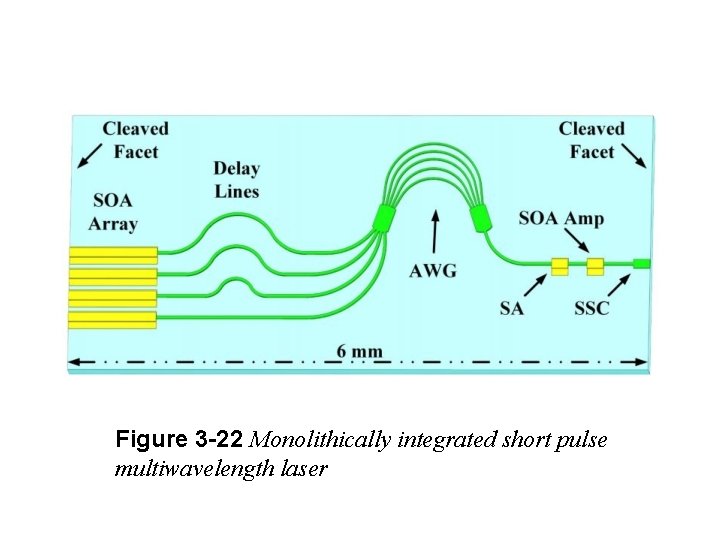
Figure 3 -22 Monolithically integrated short pulse multiwavelength laser

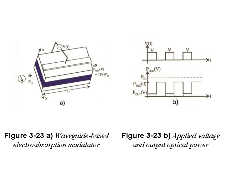
Figure 3 -23 a) Waveguide-based electroabsorption modulator Figure 3 -23 b) Applied voltage and output optical power

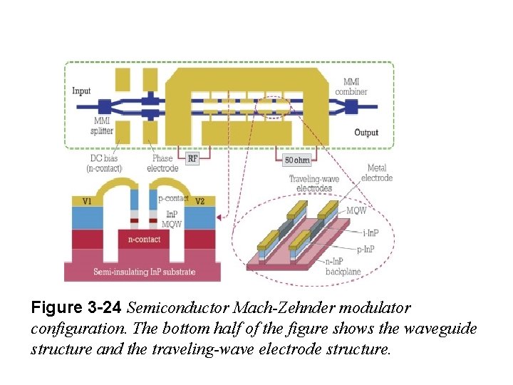
Figure 3 -24 Semiconductor Mach-Zehnder modulator configuration. The bottom half of the figure shows the waveguide structure and the traveling-wave electrode structure.

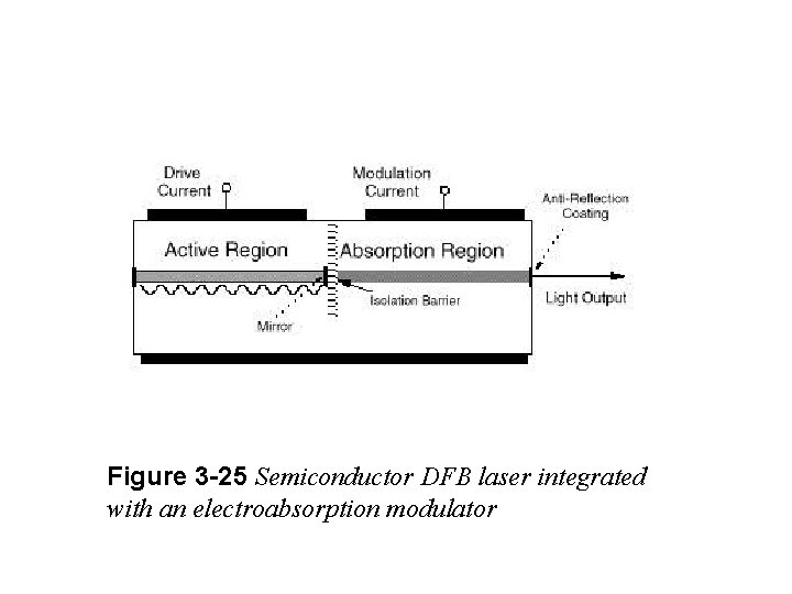
Figure 3 -25 Semiconductor DFB laser integrated with an electroabsorption modulator

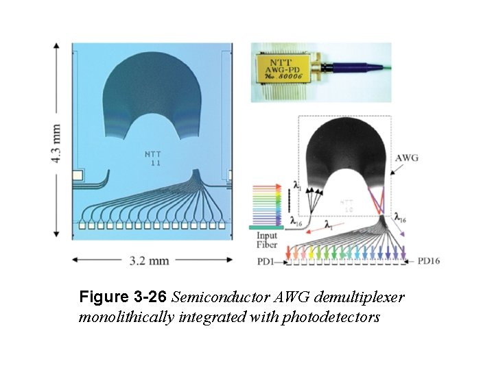
Figure 3 -26 Semiconductor AWG demultiplexer monolithically integrated with photodetectors