ILC ELECTRON SOURCE SUMMARY M Kuriki J Grames



- Slides: 23

ILC ELECTRON SOURCE SUMMARY M. Kuriki, J. Grames AWLC 2020 Source WG

CONTENTS 1 ILC Electron Source 2 PES cathode 3 Laser system 4 Summary

TDR Design 3

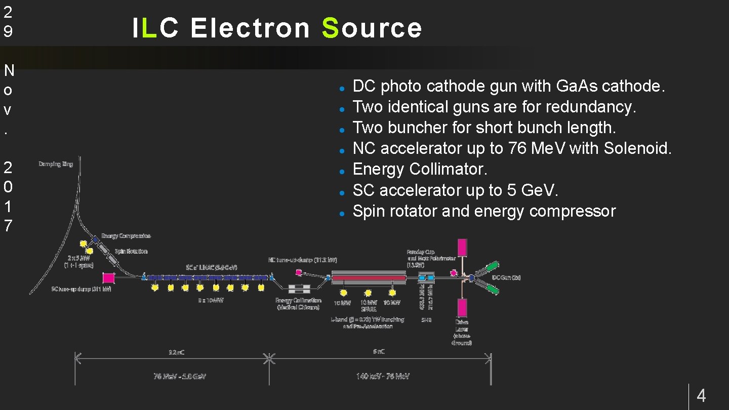
2 9 N o v. ILC Electron Source 2 0 1 7 DC photo cathode gun with Ga. As cathode. Two identical guns are for redundancy. Two buncher for short bunch length. NC accelerator up to 76 Me. V with Solenoid. Energy Collimator. SC accelerator up to 5 Ge. V. Spin rotator and energy compressor 4

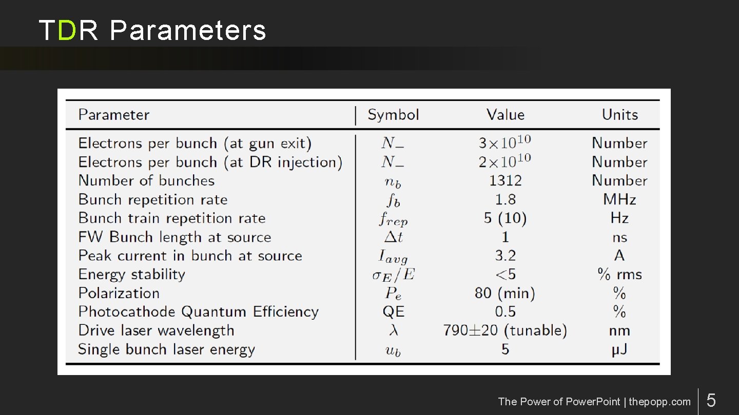
TDR Parameters The Power of Power. Point | thepopp. com 5

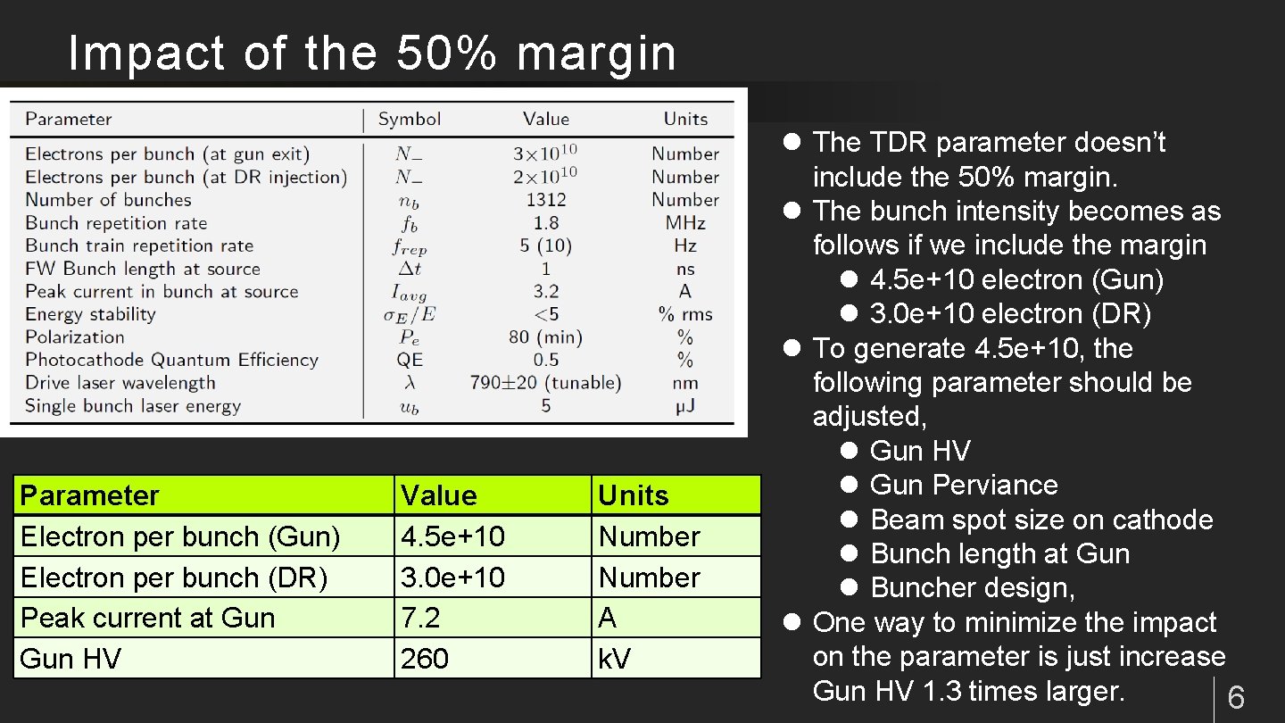
Impact of the 50% margin Parameter Electron per bunch (Gun) Electron per bunch (DR) Peak current at Gun HV Value 4. 5 e+10 3. 0 e+10 7. 2 260 Units Number A k. V The TDR parameter doesn’t include the 50% margin. The bunch intensity becomes as follows if we include the margin 4. 5 e+10 electron (Gun) 3. 0 e+10 electron (DR) To generate 4. 5 e+10, the following parameter should be adjusted, Gun HV Gun Perviance Beam spot size on cathode Bunch length at Gun Buncher design, One way to minimize the impact on the parameter is just increase Gun HV 1. 3 times larger. 6

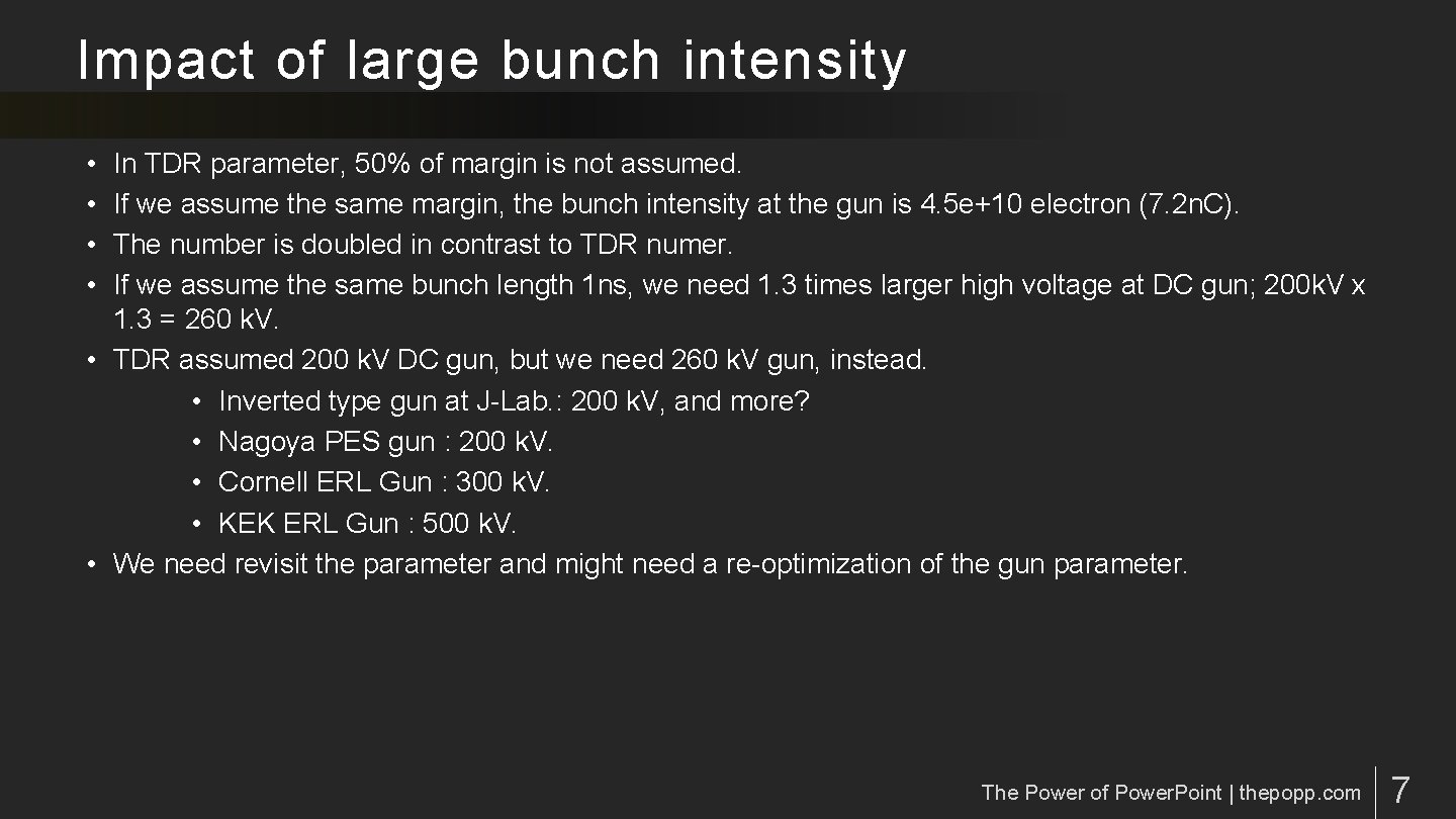
Impact of large bunch intensity • • In TDR parameter, 50% of margin is not assumed. If we assume the same margin, the bunch intensity at the gun is 4. 5 e+10 electron (7. 2 n. C). The number is doubled in contrast to TDR numer. If we assume the same bunch length 1 ns, we need 1. 3 times larger high voltage at DC gun; 200 k. V x 1. 3 = 260 k. V. • TDR assumed 200 k. V DC gun, but we need 260 k. V gun, instead. • Inverted type gun at J-Lab. : 200 k. V, and more? • Nagoya PES gun : 200 k. V. • Cornell ERL Gun : 300 k. V. • KEK ERL Gun : 500 k. V. • We need revisit the parameter and might need a re-optimization of the gun parameter. The Power of Power. Point | thepopp. com 7

PES Cathode 8

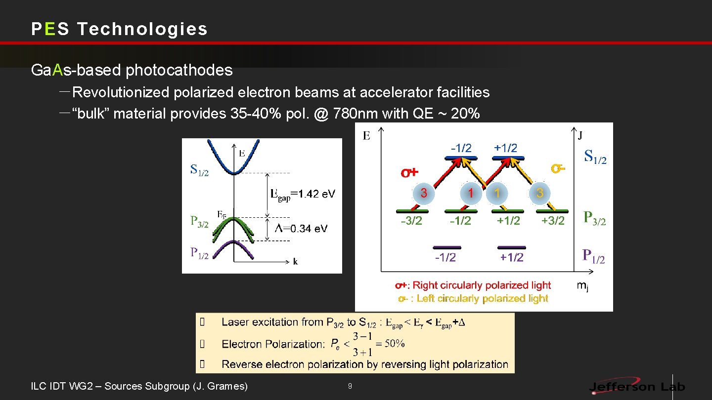
PES Technologies Ga. As-based photocathodes -Revolutionized polarized electron beams at accelerator facilities -“bulk” material provides 35 -40% pol. @ 780 nm with QE ~ 20% ILC IDT WG 2 – Sources Subgroup (J. Grames) 9

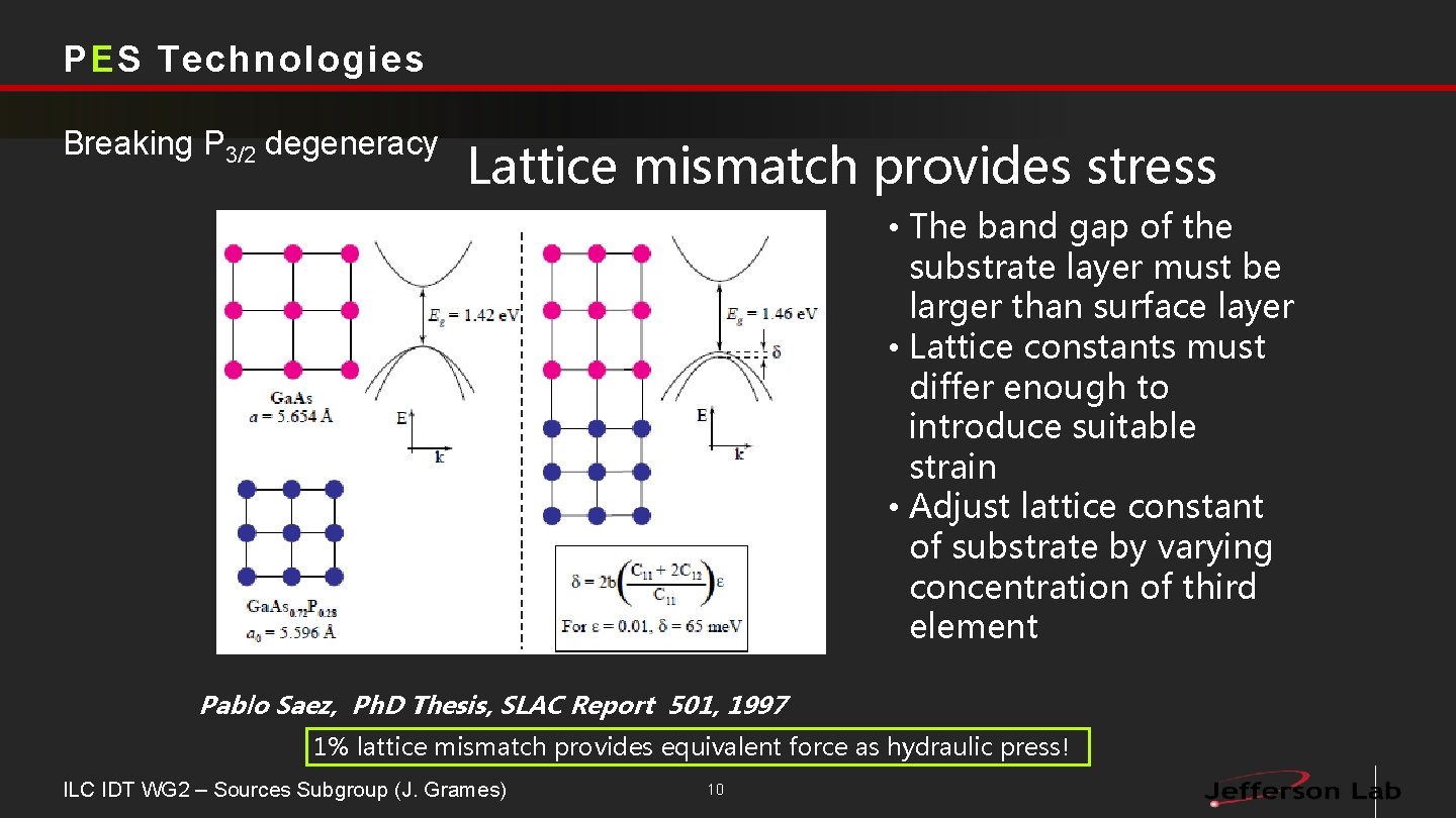
PES Technologies Breaking P 3/2 degeneracy Lattice mismatch provides stress • The band gap of the substrate layer must be larger than surface layer • Lattice constants must differ enough to introduce suitable strain • Adjust lattice constant of substrate by varying concentration of third element Pablo Saez, Ph. D Thesis, SLAC Report 501, 1997 1% lattice mismatch provides equivalent force as hydraulic press! ILC IDT WG 2 – Sources Subgroup (J. Grames) 10

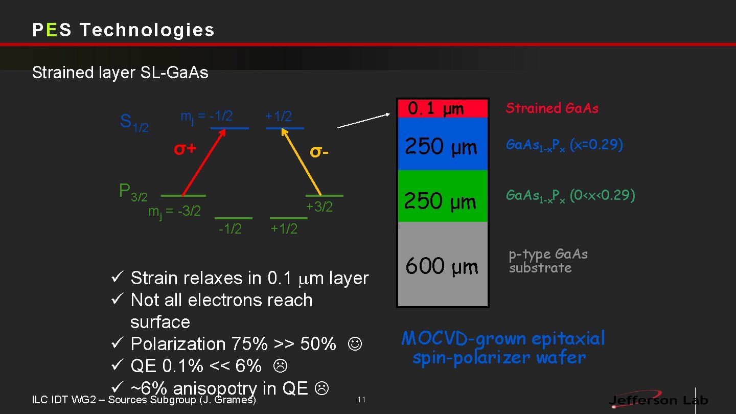
PES Technologies Strained layer SL-Ga. As S 1/2 mj = -1/2 +1/2 σ+ P 3/2 mj = -3/2 σ+3/2 -1/2 0. 1 μm Strained Ga. As 250 μm Ga. As 1 -x. Px (x=0. 29) 250 μm Ga. As 1 -x. Px (0<x<0. 29) 600 μm p-type Ga. As substrate +1/2 ü Strain relaxes in 0. 1 mm layer ü Not all electrons reach surface ü Polarization 75% >> 50% ü QE 0. 1% << 6% ü ~6% anisopotry in QE 11 ILC IDT WG 2 – Sources Subgroup (J. Grames) MOCVD-grown epitaxial spin-polarizer wafer

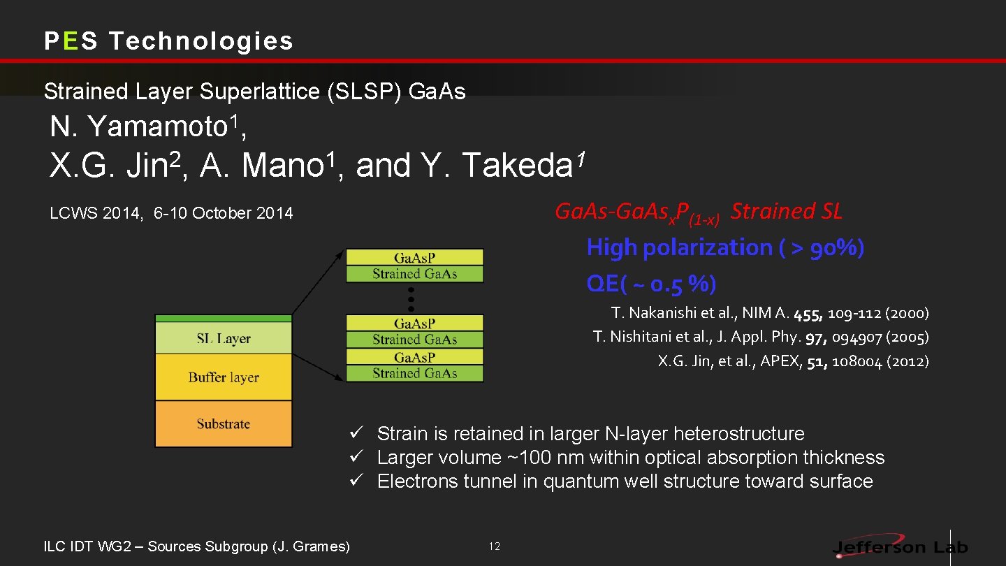
PES Technologies Strained Layer Superlattice (SLSP) Ga. As N. Yamamoto 1, X. G. 2 Jin , A. 1 Mano , and Y. 1 Takeda Ga. As-Ga. Asx. P(1 -x) Strained SL High polarization ( > 90%) QE( ~ 0. 5 %) LCWS 2014, 6 -10 October 2014 T. Nakanishi et al. , NIM A. 455, 109 -112 (2000) T. Nishitani et al. , J. Appl. Phy. 97, 094907 (2005) X. G. Jin, et al. , APEX, 51, 108004 (2012) ü Strain is retained in larger N-layer heterostructure ü Larger volume ~100 nm within optical absorption thickness ü Electrons tunnel in quantum well structure toward surface ILC IDT WG 2 – Sources Subgroup (J. Grames) 12

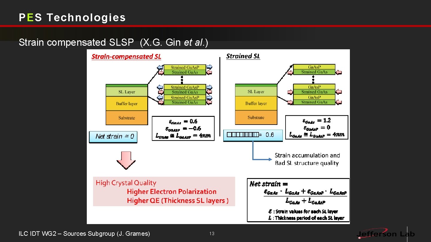
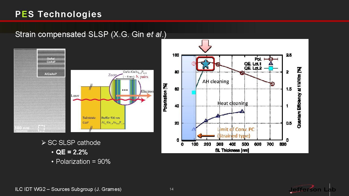
PES Technologies Strain compensated SLSP (X. G. Gin et al. ) ILC IDT WG 2 – Sources Subgroup (J. Grames) 13

PES Technologies Strain compensated SLSP (X. G. Gin et al. ) Ø SC SLSP cathode • QE = 2. 2% • Polarization = 90% ILC IDT WG 2 – Sources Subgroup (J. Grames) 14

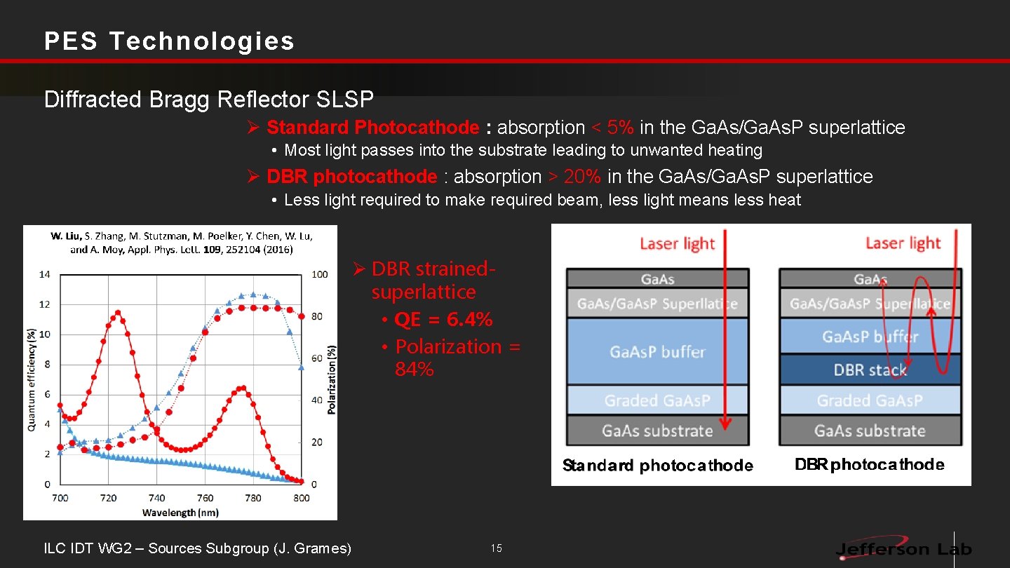
PES Technologies Diffracted Bragg Reflector SLSP Ø Standard Photocathode : absorption < 5% in the Ga. As/Ga. As. P superlattice • Most light passes into the substrate leading to unwanted heating Ø DBR photocathode : absorption > 20% in the Ga. As/Ga. As. P superlattice • Less light required to make required beam, less light means less heat Ø DBR strainedsuperlattice • QE = 6. 4% • Polarization = 84% ILC IDT WG 2 – Sources Subgroup (J. Grames) 15

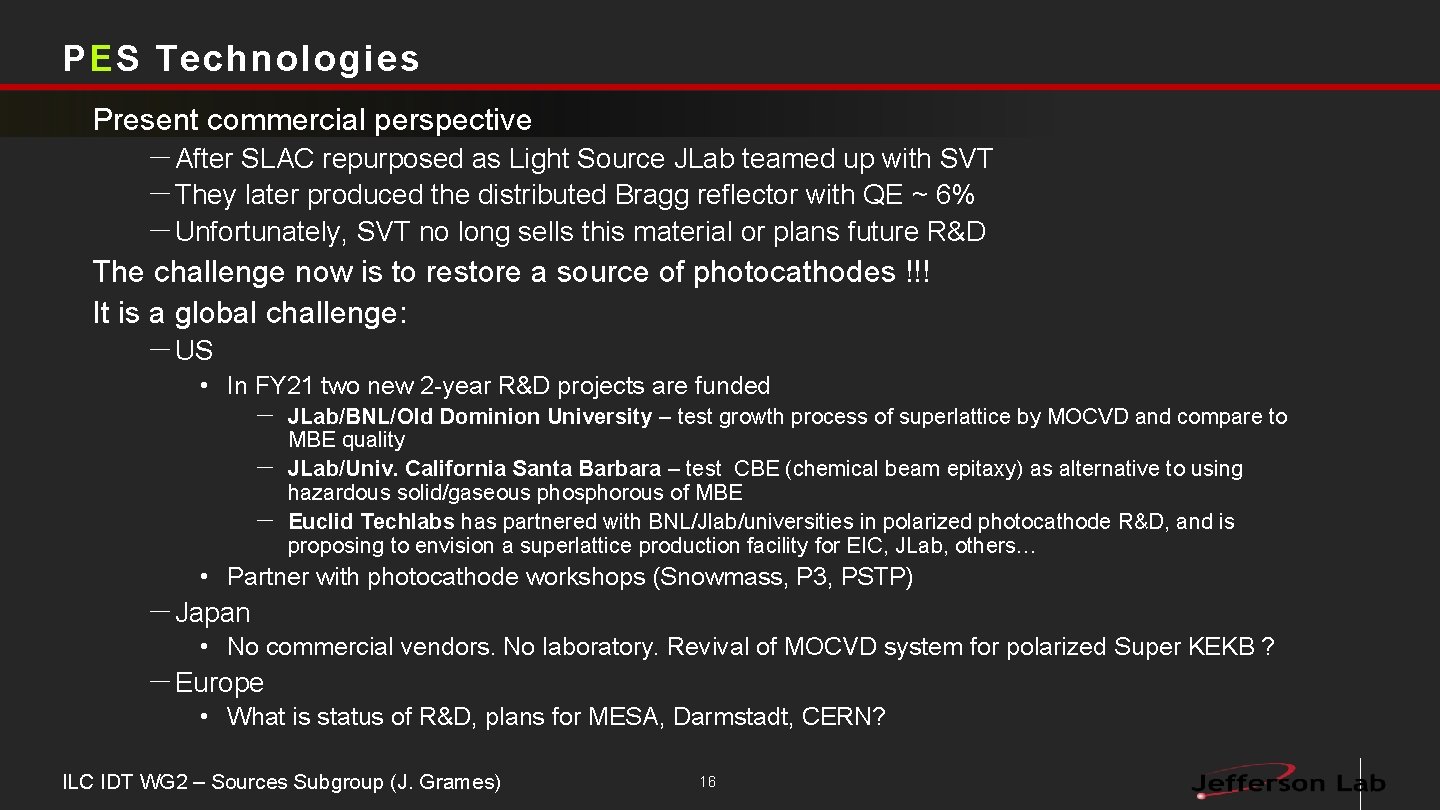
PES Technologies Present commercial perspective -After SLAC repurposed as Light Source JLab teamed up with SVT -They later produced the distributed Bragg reflector with QE ~ 6% -Unfortunately, SVT no long sells this material or plans future R&D The challenge now is to restore a source of photocathodes !!! It is a global challenge: -US • In FY 21 two new 2 -year R&D projects are funded - JLab/BNL/Old Dominion University – test growth process of superlattice by MOCVD and compare to MBE quality - JLab/Univ. California Santa Barbara – test CBE (chemical beam epitaxy) as alternative to using hazardous solid/gaseous phosphorous of MBE - Euclid Techlabs has partnered with BNL/Jlab/universities in polarized photocathode R&D, and is proposing to envision a superlattice production facility for EIC, JLab, others… • Partner with photocathode workshops (Snowmass, P 3, PSTP) -Japan • No commercial vendors. No laboratory. Revival of MOCVD system for polarized Super KEKB ? -Europe • What is status of R&D, plans for MESA, Darmstadt, CERN? ILC IDT WG 2 – Sources Subgroup (J. Grames) 16

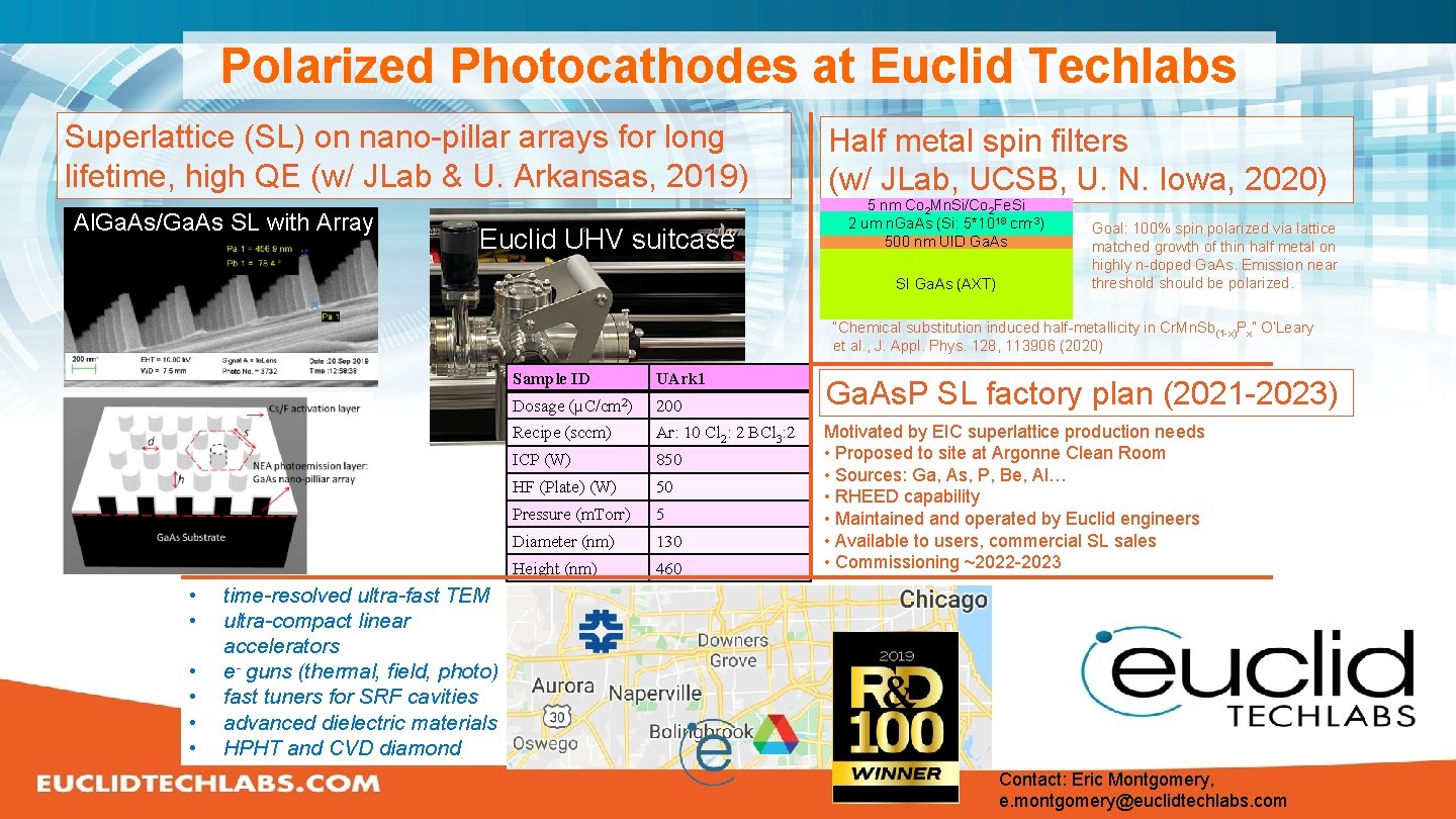
Polarized Photocathodes at Euclid Techlabs Superlattice (SL) on nano-pillar arrays for long lifetime, high QE (w/ JLab & U. Arkansas, 2019) Al. Ga. As/Ga. As SL with Array Euclid UHV suitcase Half metal spin filters (w/ JLab, UCSB, U. N. Iowa, 2020) 5 nm Co 2 Mn. Si/Co 2 Fe. Si 2 um n. Ga. As (Si: 5*1018 cm-3) 500 nm UID Ga. As SI Ga. As (AXT) Goal: 100% spin polarized via lattice matched growth of thin half metal on highly n-doped Ga. As. Emission near threshold should be polarized. “Chemical substitution induced half-metallicity in Cr. Mn. Sb(1 -x)Px” O’Leary et al. , J. Appl. Phys. 128, 113906 (2020) • • • Sample ID UArk 1 Dosage (µC/cm 2) 200 Recipe (sccm) Ar: 10 Cl 2: 2 BCl 3: 2 ICP (W) 850 HF (Plate) (W) 50 Pressure (m. Torr) 5 Diameter (nm) 130 Height (nm) 460 Ga. As. P SL factory plan (2021 -2023) Motivated by EIC superlattice production needs • Proposed to site at Argonne Clean Room • Sources: Ga, As, P, Be, Al… • RHEED capability • Maintained and operated by Euclid engineers • Available to users, commercial SL sales • Commissioning ~2022 -2023 time-resolved ultra-fast TEM ultra-compact linear accelerators e- guns (thermal, field, photo) fast tuners for SRF cavities advanced dielectric materials HPHT and CVD diamond Contact: Eric Montgomery, e. montgomery@euclidtechlabs. com

Laser System 18

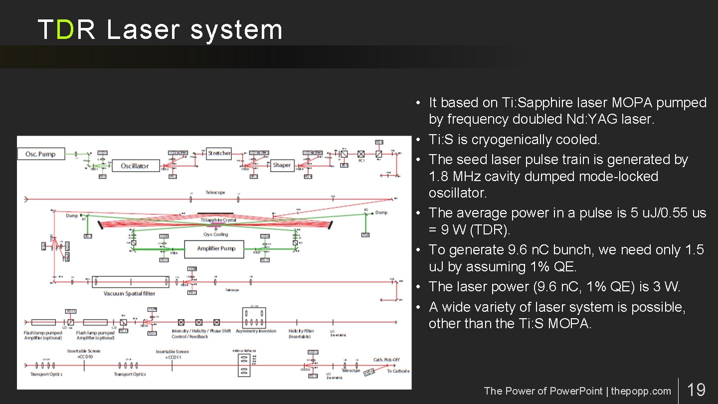
TDR Laser system • It based on Ti: Sapphire laser MOPA pumped by frequency doubled Nd: YAG laser. • Ti: S is cryogenically cooled. • The seed laser pulse train is generated by 1. 8 MHz cavity dumped mode-locked oscillator. • The average power in a pulse is 5 u. J/0. 55 us = 9 W (TDR). • To generate 9. 6 n. C bunch, we need only 1. 5 u. J by assuming 1% QE. • The laser power (9. 6 n. C, 1% QE) is 3 W. • A wide variety of laser system is possible, other than the Ti: S MOPA. The Power of Power. Point | thepopp. com 19

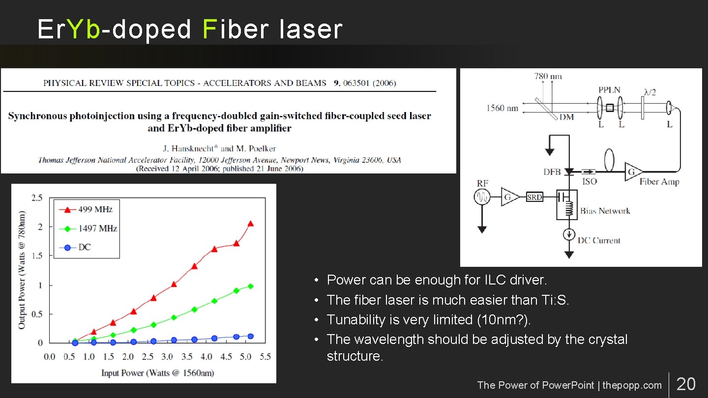
Er. Yb-doped Fiber laser • • Power can be enough for ILC driver. The fiber laser is much easier than Ti: S. Tunability is very limited (10 nm? ). The wavelength should be adjusted by the crystal structure. The Power of Power. Point | thepopp. com 20

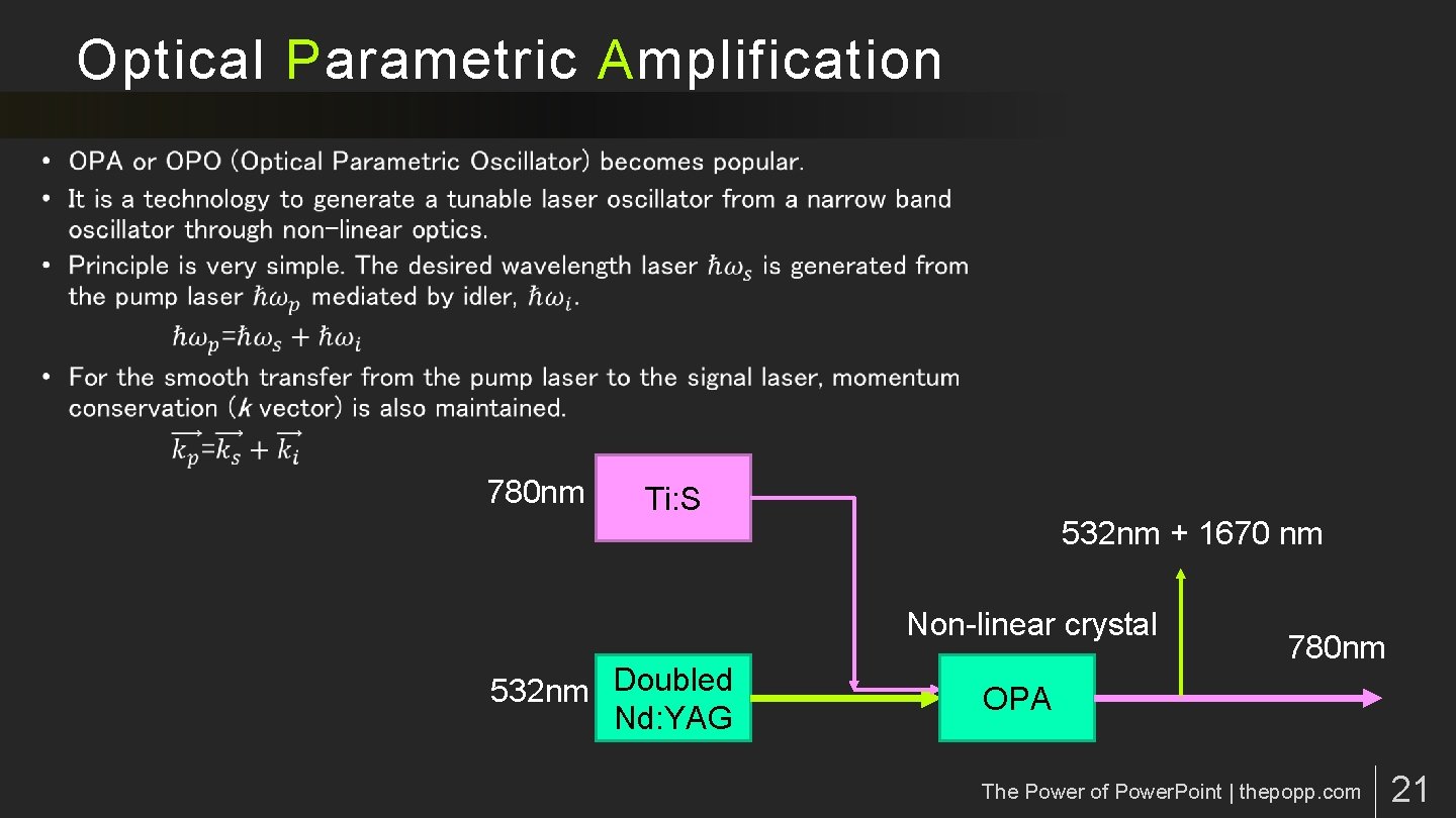
Optical Parametric Amplification 780 nm Ti: S 532 nm + 1670 nm Non-linear crystal 532 nm Doubled Nd: YAG 780 nm OPA The Power of Power. Point | thepopp. com 21

Summary • Summary of ILC Electron source is presented. • TDR parameter doesn’t have any margin on DR bunch. If we assume the 50% margin, the bunch intensity from the gun is 7. 2 n. C (assuming 50% transmission). • Need a higher voltage gun, 260 k. V to keep the 1 ns bunch length from the gun, otherwise, we need to re-design the injector (buncher). • Cathode technology is progressed giving a high polarization with a higher QE. • Cathode supply system should be established. • A wide variety solutions are possible for the laser system employing the latest laser technology.

THANK YOU! Any Questions?