IAEA Post Graduate Educational Course Radiation Protection and
- Slides: 22

IAEA Post Graduate Educational Course Radiation Protection and Safe Use of Radiation Sources Part IIQuantities and Measurements Module 3 Principles of Radiation Detection and Measurements Session 6 Semiconductor detectors IAEA International Atomic Energy Agency

Semiconductor Detectors • Upon completion of this section the student will be able to explain the process and characteristics of semiconductor detectors including the concepts: • • • N-type P-type Intrinsic/Depletion region Resolution Efficiency IAEA 2

Semiconductor Diodes • Semiconductors are typically made of silicon or germanium • For portable detectors, silicon is typically used because the band gap is greater which results in less thermally generated “noise” • To reduce this noise in germanium detectors it is necessary to cool the detectors using liquid nitrogen IAEA 3

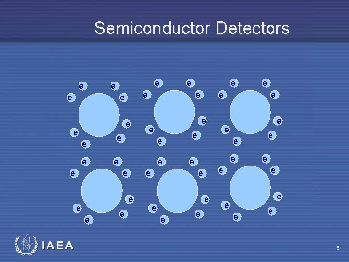
Semiconductor Detectors • Silicon forms a crystal that has a diamond shaped lattice • Each silicon atom has four covalent bonds • In the diagram in the next slide, each covalent bond is represented by a pair of valence band electrons IAEA 4

Semiconductor Detectors e e e e e e e e e IAEA e e e e 5

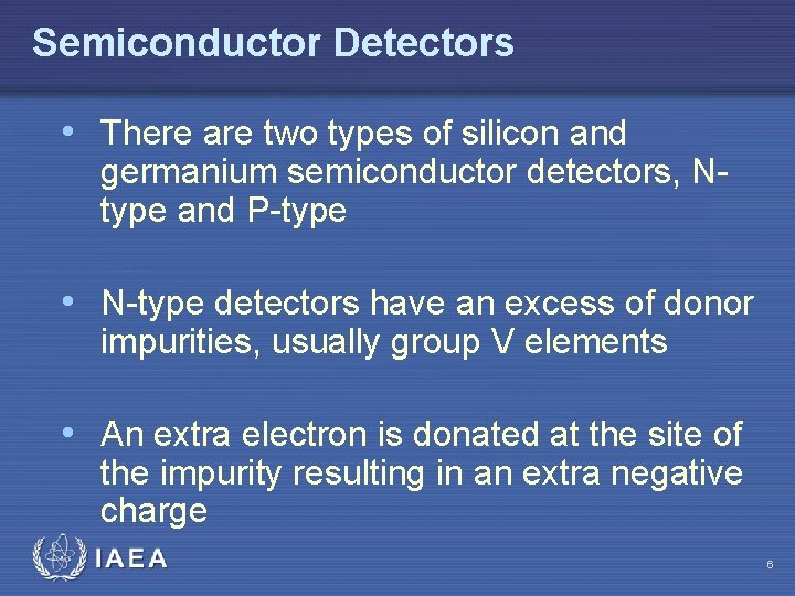
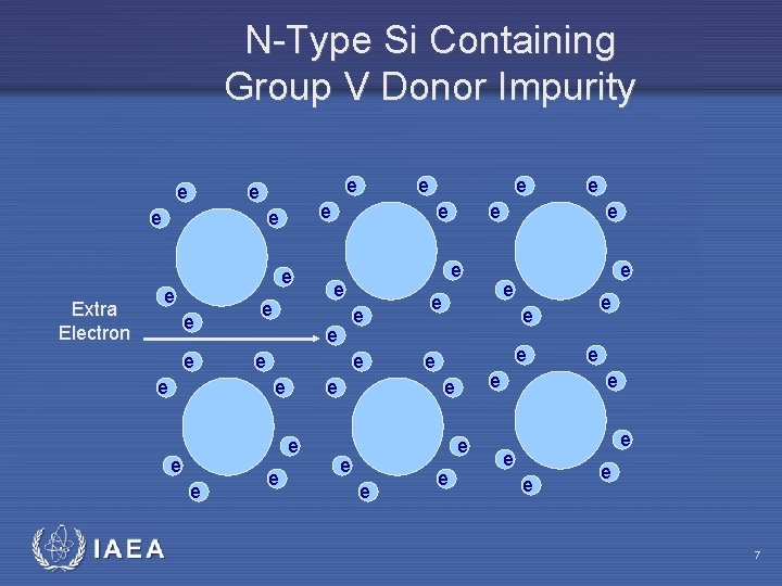
Semiconductor Detectors • There are two types of silicon and germanium semiconductor detectors, Ntype and P-type • N-type detectors have an excess of donor impurities, usually group V elements • An extra electron is donated at the site of the impurity resulting in an extra negative charge IAEA 6

N-Type Si Containing Group V Donor Impurity e e Extra Electron e e e e e e e e IAEA e e e e 7

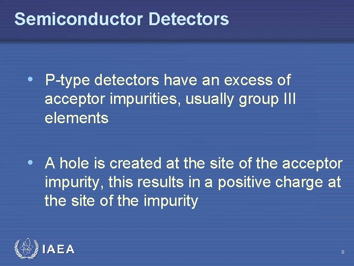
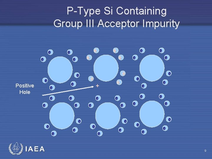
Semiconductor Detectors • P-type detectors have an excess of acceptor impurities, usually group III elements • A hole is created at the site of the acceptor impurity, this results in a positive charge at the site of the impurity IAEA 8

P-Type Si Containing Group III Acceptor Impurity e e Positive Hole e e e e e e + e e IAEA e e e e 9

Semiconductor Detectors • The sensitive volume of a diode detector is referred to as the depletion or intrinsic region • This is the region of relative purity at a junction of n-type and p-type semiconductor material • At this junction, the electrons from the n-type silicon migrate across the junction and fill the holes in the ptype silicon to create the p-n junction where there is no excess of holes or electrons IAEA 10

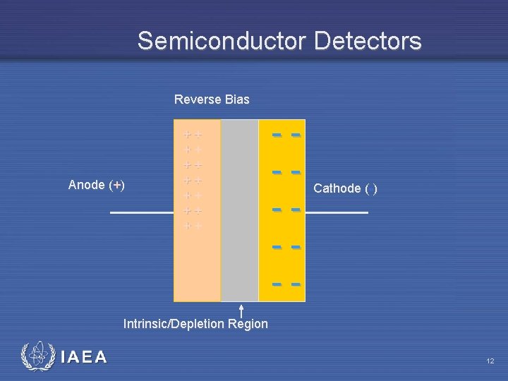
Semiconductor Detectors • When a positive voltage is applied to the n-type material and negative voltage to the p-type material, the electrons are pulled further away from this region creating a much thicker depletion region • The depletion region acts as the sensitive volume of the detector • Ionizing radiation entering this region will create holes and excess electrons which migrate and cause an electrical pulse IAEA 11

Semiconductor Detectors Reverse Bias Anode (+) ++ ++ ------ Cathode (-) Intrinsic/Depletion Region IAEA 12

Semiconductor Detectors • Diode detectors are often referred to as “PIN” detectors or diodes. “PIN” is from P-type, Intrinsic region, N-type • The intrinsic region is several hundred micrometers thick • The intrinsic efficiency (ignoring attenuation from the housing) is 100% for 10 ke. V photons IAEA 13

Semiconductor Detectors • The efficiency is reduced to approximately 1% for 150 ke. V photons and remains more or less constant above this energy • Above 60 ke. V, the interactions involve Compton scattering almost exclusively IAEA 14

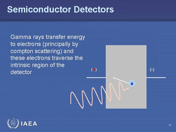
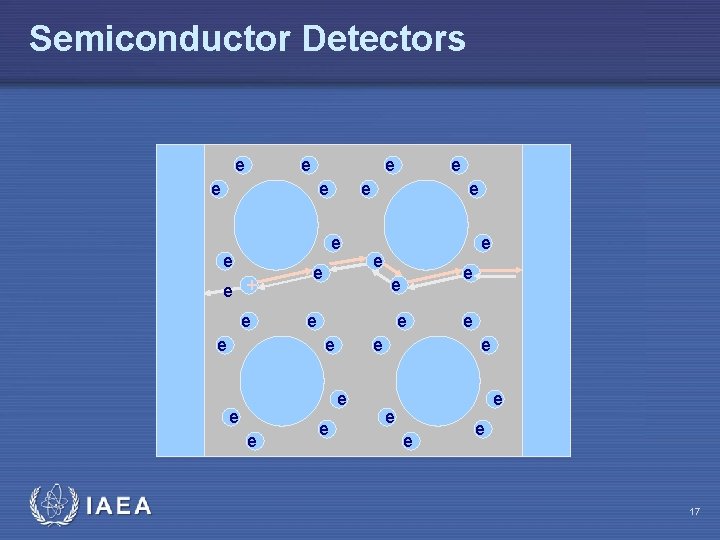
Semiconductor Detectors Gamma rays transfer energy to electrons (principally by compton scattering) and these electrons traverse the intrinsic region of the detector (+ ) (-) e IAEA 15

Semiconductor Detectors • When a charged particle traverses the intrinsic (depletion) region, electrons are promoted from the valence band to the conduction band • This results in a hole in the valence band • Once in the conduction band, the electron is mobile and it moves to the anode while the positive hole moves to the cathode (actually it is displaced by electrons moving to the anode) IAEA 16

Semiconductor Detectors e e e + e e e e IAEA e e e 17

Semiconductor Detectors • The average energy needed to create an electron-hole pair in silicon is about 3. 6 e. V. • The average needed to create an ion pair in gas is about 34 e. V, so for the same energy deposited, we get about 34/3. 6 or about 9 times more charged pairs. IAEA 18

Energy Resolution • The energy resolution in a detector is E/E, which is proportional to N where N is the number of charged pairs • Using a semiconductor detector, we receive about 9, or 3 times the resolution of a gas ionization detector system • Compared to a scintillation detector which requires about 1000 e. V to create one photoelectron at the PM tube, the resolution is about 17 times better IAEA 19

Germanium vs Silicon Detectors • Germanium (Ge) requires only 2. 9 e. V to create an electron-hole pair vs. 3. 6 e. V for silicon, so the energy resolution is (3. 6/2. 9) = 1. 1 times that of silicon • The problem with Ge is that thermal excitation creates electron-hole pairs. For this reason liquid nitrogen is used to cool the electronics of germanium systems IAEA 20

Ge(Li) and Si(Li) Detectors • Germanium with lithium ions used to create the depletion zone form what is known as a Ge(Li) “jelly” detector • Silicon with lithium ions used to create the depletion zone comprise what is known as a Si(Li) “silly” detector IAEA 21

Ge(Li) and Si(Li) Detectors • For gamma ray detection, the detector efficiency for the photoelectric effect is proportional to Z 5, where Z is the atomic number of the detector material • Since for Ge, Z=32, and the Z of Si is 14, Ge detectors are about 62 times more efficient than Si detectors IAEA 22