Development of resistive Micromegas TPCs for the T
- Slides: 26

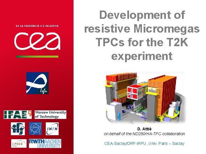
Development of resistive Micromegas TPCs for the T 2 K experiment D. Attié on behalf of the ND 280/HA-TPC collaboration CEA-Saclay/DRF-IRFU, Univ. Paris – Saclay

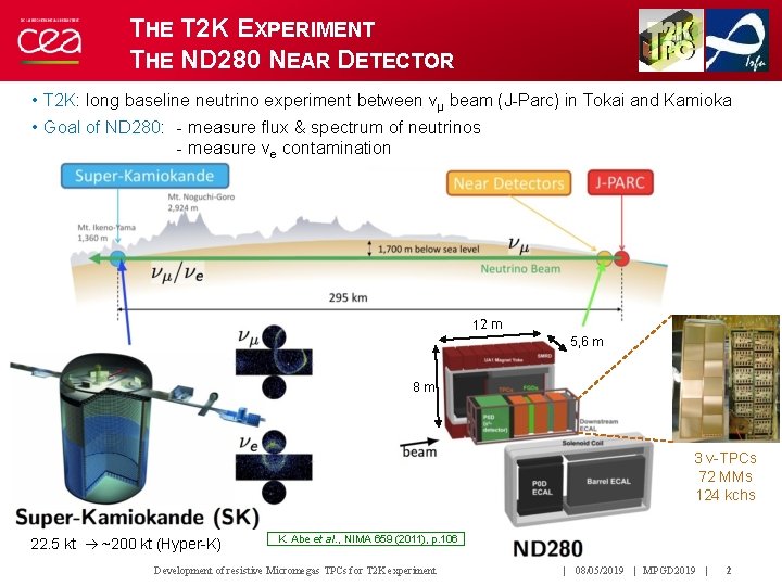
THE T 2 K EXPERIMENT THE ND 280 NEAR DETECTOR • T 2 K: long baseline neutrino experiment between νμ beam (J-Parc) in Tokai and Kamioka • Goal of ND 280: - measure flux & spectrum of neutrinos - measure νe contamination 12 m 5, 6 m 8 m 3 v-TPCs 72 MMs 124 kchs 22. 5 kt ~200 kt (Hyper-K) K. Abe et al. , NIMA 659 (2011), p. 106 Development of resistive Micromegas TPCs for T 2 K experiment | 08/05/2019 | MPGD 2019 | 2

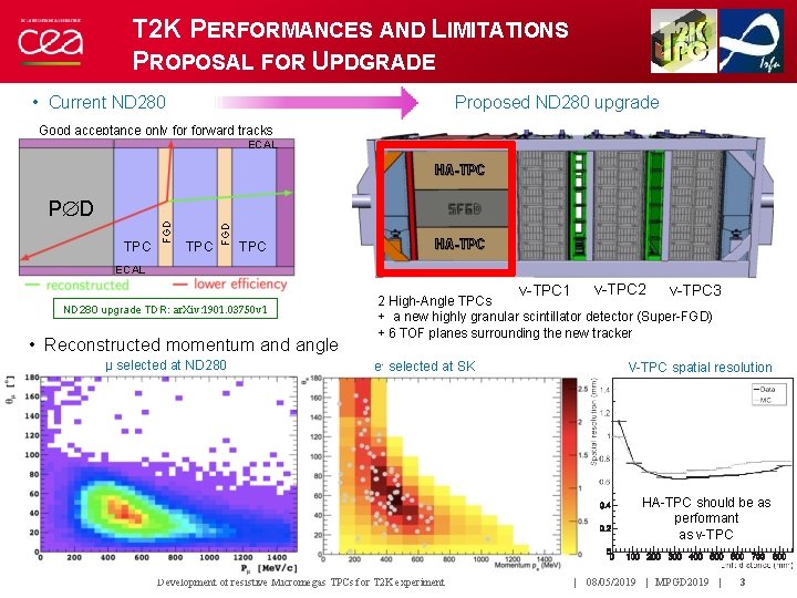
T 2 K PERFORMANCES AND LIMITATIONS PROPOSAL FOR UPDGRADE • Current ND 280 Proposed ND 280 upgrade Good acceptance only forward tracks ECAL TPC FGD P D FGD HA-TPC ECAL v-TPC 1 ND 280 upgrade TDR: ar. Xiv: 1901. 03750 v 1 • Reconstructed momentum and angle µ selected at ND 280 v-TPC 2 v-TPC 3 2 High-Angle TPCs + a new highly granular scintillator detector (Super-FGD) + 6 TOF planes surrounding the new tracker e- selected at SK V-TPC spatial resolution HA-TPC should be as performant as v-TPC Development of resistive Micromegas TPCs for T 2 K experiment | 08/05/2019 | MPGD 2019 | 3

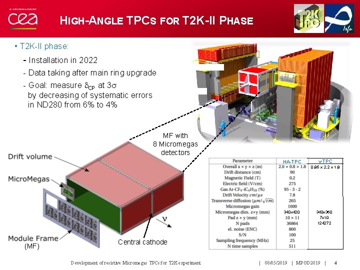
HIGH-ANGLE TPCS FOR T 2 K-II PHASE • T 2 K-II phase: - Installation in 2022 - Data taking after main ring upgrade - Goal: measure CP at 3 by decreasing of systematic errors in ND 280 from 6% to 4% MF with 8 Micromegas detectors HA-TPC v-TPC 0. 85 x 2. 2 x 1. 8 340 x 420 (MF) 340 x 360 7 x 10 124272 Central cathode Development of resistive Micromegas TPCs for T 2 K experiment | 08/05/2019 | MPGD 2019 | 4

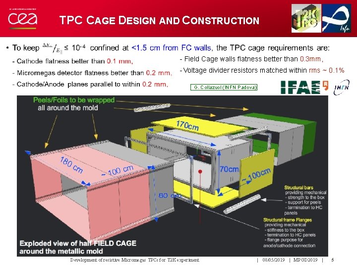
TPC CAGE DESIGN AND CONSTRUCTION - Field Cage walls flatness better than 0. 3 mm, - Voltage divider resistors matched within rms ~ 0. 1% G. Collazuol (INFN Padova) Development of resistive Micromegas TPCs for T 2 K experiment | 08/05/2019 | MPGD 2019 | 5

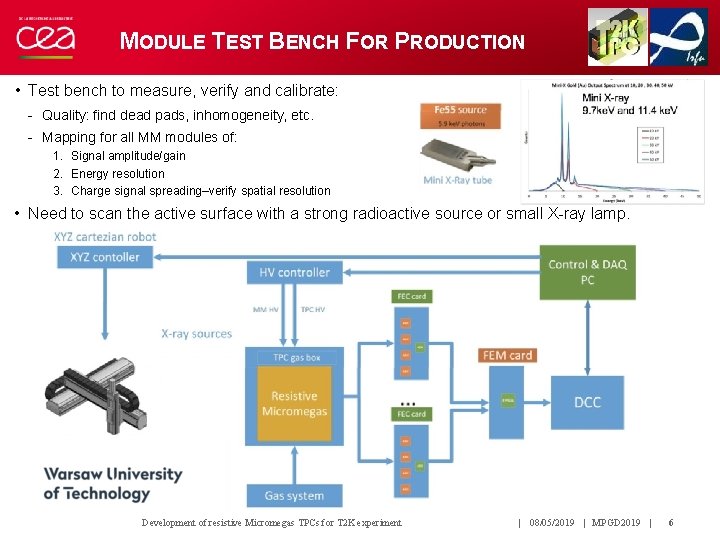
MODULE TEST BENCH FOR PRODUCTION • Test bench to measure, verify and calibrate: - Quality: find dead pads, inhomogeneity, etc. - Mapping for all MM modules of: 1. Signal amplitude/gain 2. Energy resolution 3. Charge signal spreading–verify spatial resolution • Need to scan the active surface with a strong radioactive source or small X-ray lamp. Development of resistive Micromegas TPCs for T 2 K experiment | 08/05/2019 | MPGD 2019 | 6

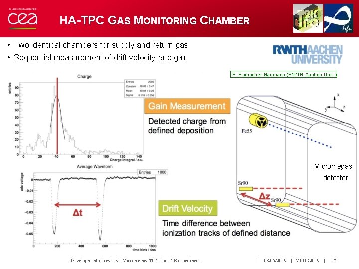
HA-TPC GAS MONITORING CHAMBER • Two identical chambers for supply and return gas • Sequential measurement of drift velocity and gain P. Hamacher-Baumann (RWTH Aachen Univ. ) Micromegas detector Development of resistive Micromegas TPCs for T 2 K experiment | 08/05/2019 | MPGD 2019 | 7

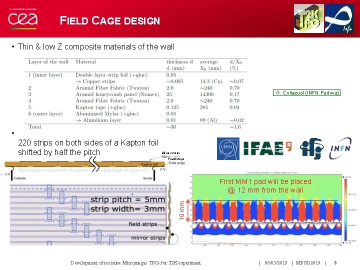
FIELD CAGE DESIGN • Thin & low Z composite materials of the wall G. Collazuol (INFN Padova) • 220 strips on both sides of a Kapton foil shifted by half the pitch Mirror strips Field strips 10 mm First MM 1 pad will be placed @ 12 mm from the wall Development of resistive Micromegas TPCs for T 2 K experiment | 08/05/2019 | MPGD 2019 | 8

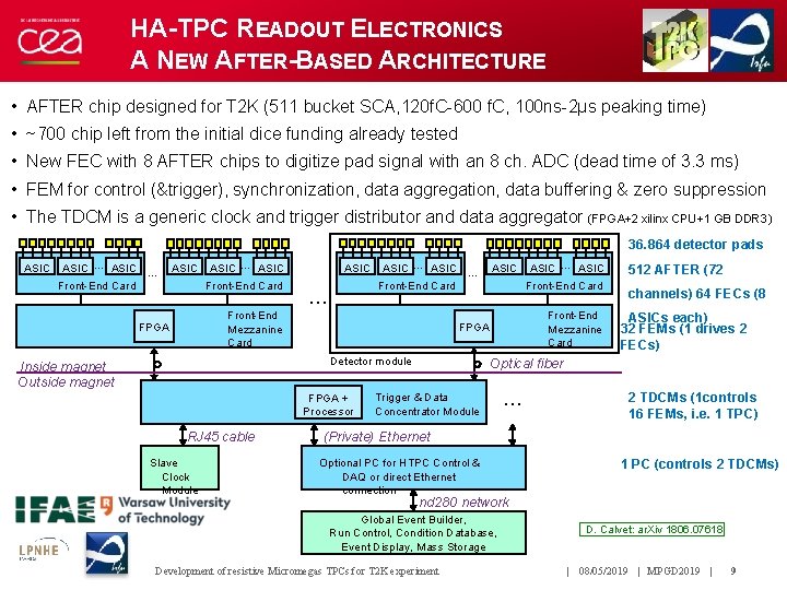
HA-TPC READOUT ELECTRONICS A NEW AFTER-BASED ARCHITECTURE • AFTER chip designed for T 2 K (511 bucket SCA, 120 f. C-600 f. C, 100 ns-2µs peaking time) • ~700 chip left from the initial dice funding already tested • New FEC with 8 AFTER chips to digitize pad signal with an 8 ch. ADC (dead time of 3. 3 ms) • FEM for control (&trigger), synchronization, data aggregation, data buffering & zero suppression • The TDCM is a generic clock and trigger distributor and data aggregator (FPGA+2 xilinx CPU+1 GB DDR 3) 36. 864 detector pads ASIC … Front-End Card ASIC … ASIC … Front-End Card Front-End Mezzanine Card FPGA + Processor RJ 45 cable Slave Clock Module ASIC … ASIC Front-End Card Front-End Mezzanine Card FPGA Detector module Inside magnet Outside magnet ASIC 512 AFTER (72 channels) 64 FECs (8 ASICs each) 32 FEMs (1 drives 2 FECs) Optical fiber Trigger & Data Concentrator Module … 2 TDCMs (1 controls 16 FEMs, i. e. 1 TPC) (Private) Ethernet Optional PC for HTPC Control & DAQ or direct Ethernet connection 1 PC (controls 2 TDCMs) nd 280 network Global Event Builder, Run Control, Condition Database, Event Display, Mass Storage Development of resistive Micromegas TPCs for T 2 K experiment D. Calvet: ar. Xiv 1806. 07618 | 08/05/2019 | MPGD 2019 | 9

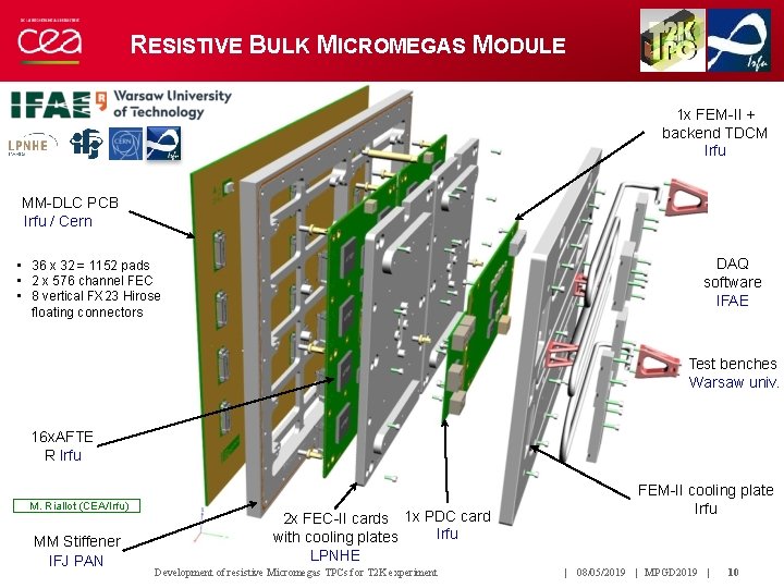
RESISTIVE BULK MICROMEGAS MODULE 1 x FEM-II + backend TDCM Irfu MM-DLC PCB Irfu / Cern DAQ software IFAE • 36 x 32 = 1152 pads • 2 x 576 channel FEC • 8 vertical FX 23 Hirose floating connectors Test benches Warsaw univ. 16 x. AFTE R Irfu M. Riallot (CEA/Irfu) MM Stiffener IFJ PAN 2 x FEC-II cards 1 x PDC card Irfu with cooling plates LPNHE Development of resistive Micromegas TPCs for T 2 K experiment FEM-II cooling plate Irfu | 08/05/2019 | MPGD 2019 | 10

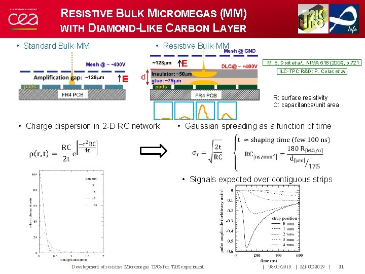
RESISTIVE BULK MICROMEGAS (MM) WITH DIAMOND-LIKE CARBON LAYER • Standard Bulk-MM • Resistive Bulk-MM M. S. Dixit et al. , NIMA 518 (2004), p. 721 ILC-TPC R&D: P. Colas et al. E R: surface resistivity C: capacitance/unit area • Charge dispersion in 2 -D RC network • Gaussian spreading as a function of time • Signals expected over contiguous strips Development of resistive Micromegas TPCs for T 2 K experiment | 08/05/2019 | MPGD 2019 | 11

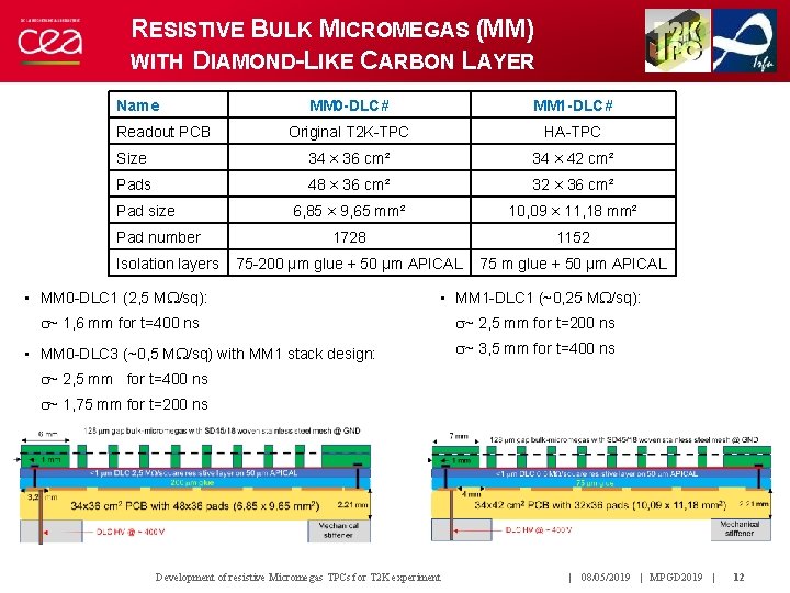
RESISTIVE BULK MICROMEGAS (MM) WITH DIAMOND-LIKE CARBON LAYER Name MM 0 -DLC# MM 1 -DLC# Original T 2 K-TPC HA-TPC Size 34 × 36 cm² 34 × 42 cm² Pads 48 × 36 cm² 32 × 36 cm² 6, 85 × 9, 65 mm² 10, 09 × 11, 18 mm² 1728 1152 75 -200 μm glue + 50 μm APICAL 75 m glue + 50 μm APICAL Readout PCB Pad size Pad number Isolation layers • MM 0 -DLC 1 (2, 5 MW/sq): • MM 1 -DLC 1 (~0, 25 MW/sq): ~ 1, 6 mm for t=400 ns • MM 0 -DLC 3 (~0, 5 MW/sq) with MM 1 stack design: ~ 2, 5 mm for t=200 ns ~ 3, 5 mm for t=400 ns ~ 2, 5 mm for t=400 ns ~ 1, 75 mm for t=200 ns Development of resistive Micromegas TPCs for T 2 K experiment | 08/05/2019 | MPGD 2019 | 12

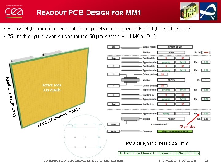
READOUT PCB DESIGN FOR MM 1 • Epoxy (~0, 02 mm) is used to fill the gap between copper pads of 10, 09 × 11, 18 mm² • 75 µm thick glue layer is used for the 50 µm Kapton + 0. 4 MΩ/□ DLC pads) f o s w (32 ro 34 cm 0. 005 Active area 1152 pads ) ads p f ns o m u l 6 co 3 ( m 42 c 75 µm glue PCB design thickness : 2. 21 mm B. Mehl, R. de Oliveira, O. Pizzirusso (CERN-EP-DT-EF) Development of resistive Micromegas TPCs for T 2 K experiment | 08/05/2019 | MPGD 2019 | 13

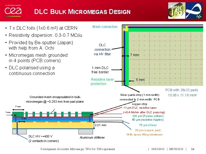
DLC BULK MICROMEGAS DESIGN Mesh connection • 7 x DLC foils (1 x 0. 6 m 2) at CERN • Resistivity dispersion: 0. 3 -0. 7 MΩ/□ • Provided by Be-sputter (Japan) with help from A. Ochi DLC connection via HV filter • Micromegas mesh grounded in 4 points (PCB corners) • DLC polarised using a continuous connection 7 mm 1 mm DLC free border Resistive layer protection 5 mm PCB with 36 x 32 pads Silver paste strip (1 mm width) Grounded mesh encapsulated in bulk- micromegas @ ~0. 253 mm from pad plane connected to 2 mm width PCB copper strip <1 µm DLC resistive layer (~0, 4 Mohm after DLC pressing) 128 µm (Pyralux plillars) 50 µm (resistive Kapton) 7 mm 1 mm 4 mm 2. 21 mm DLC HV ~+400 V (2 contacts in corners) 10. 09 x 11. 18 mm 2 Aluminum stiffener Development of resistive Micromegas TPCs for T 2 K experiment 75 µm (Glue) 35 µm (copper pad) With epoxy filling inbetween | 08/05/2019 | MPGD 2019 | 14

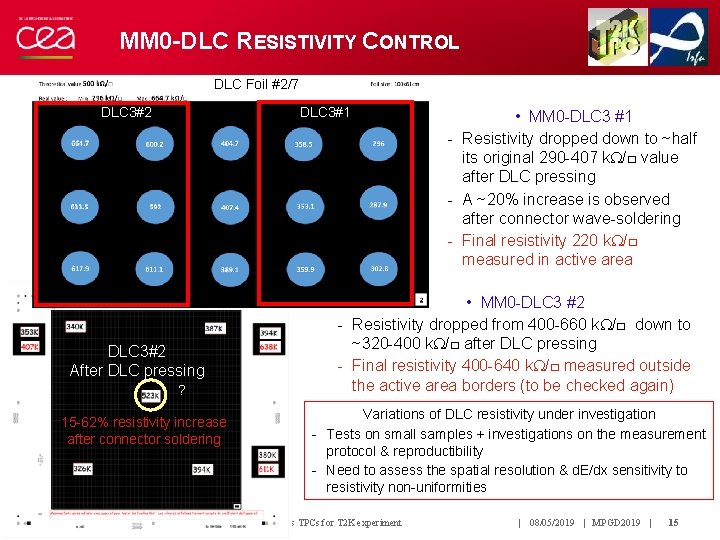
MM 0 -DLC RESISTIVITY CONTROL DLC Foil #2/7 DLC 3#2 DLC 3#1 • MM 0 -DLC 3 #1 - Resistivity dropped down to ~half its original 290 -407 k. W/□ value after DLC pressing - A ~20% increase is observed after connector wave-soldering - Final resistivity 220 k. W/□ measured in active area DLC 3#2 After DLC pressing ? 15 -62% resistivity increase after connector soldering • MM 0 -DLC 3 #2 - Resistivity dropped from 400 -660 k. W/□ down to ~320 -400 k. W/□ after DLC pressing - Final resistivity 400 -640 k. W/□ measured outside the active area borders (to be checked again) Variations of DLC resistivity under investigation - Tests on small samples + investigations on the measurement protocol & reproductibility - Need to assess the spatial resolution & d. E/dx sensitivity to resistivity non-uniformities Development of resistive Micromegas TPCs for T 2 K experiment | 08/05/2019 | MPGD 2019 | 15

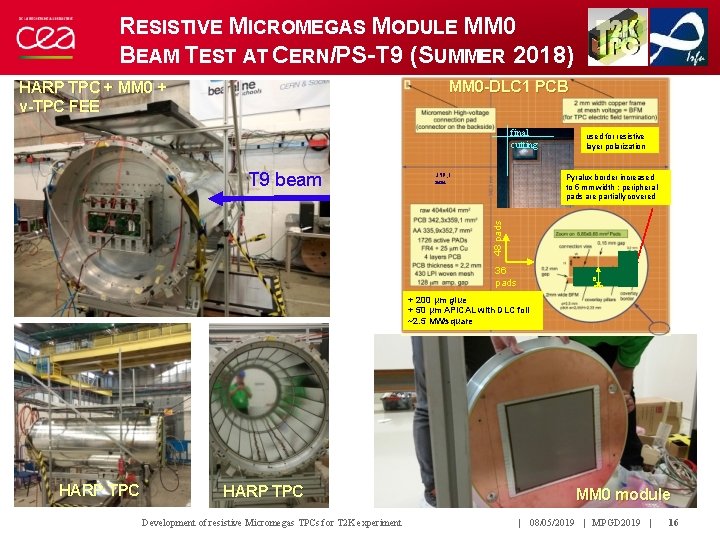
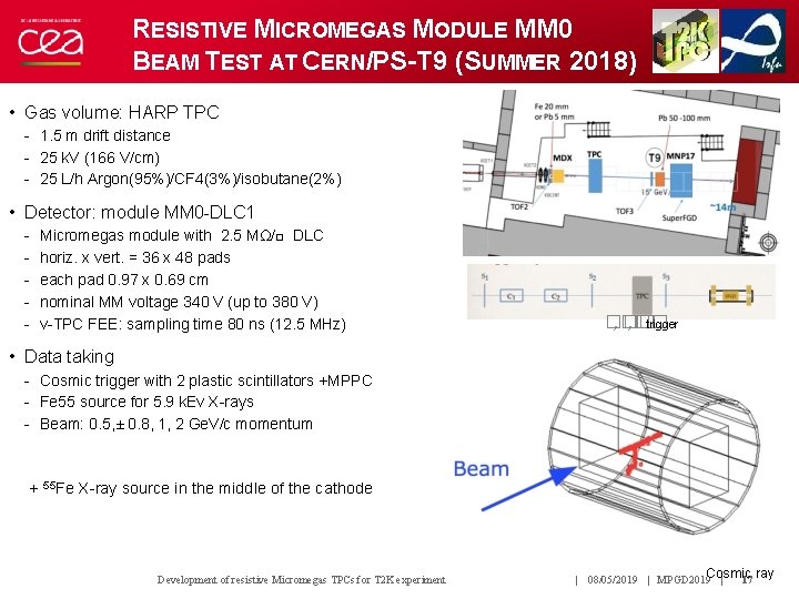
RESISTIVE MICROMEGAS MODULE MM 0 BEAM TEST AT CERN/PS-T 9 (SUMMER 2018) MM 0 -DLC 1 PCB HARP TPC + MM 0 + v-TPC FEE final cutting 359, 1 mm Pyralux border increased to 5 mm width : peripheral pads are partially covered 48 pads T 9 beam used for resistive layer polarization 36 pads 6 mm + 200 µm glue + 50 µm APICAL with DLC foil ~2. 5 MW/square HARP TPC Development of resistive Micromegas TPCs for T 2 K experiment MM 0 module | 08/05/2019 | MPGD 2019 | 16

RESISTIVE MICROMEGAS MODULE MM 0 BEAM TEST AT CERN/PS-T 9 (SUMMER 2018) • Gas volume: HARP TPC - 1. 5 m drift distance - 25 k. V (166 V/cm) - 25 L/h Argon(95%)/CF 4(3%)/isobutane(2%) • Detector: module MM 0 -DLC 1 - Micromegas module with 2. 5 MΩ/□ DLC horiz. x vert. = 36 x 48 pads each pad 0. 97 x 0. 69 cm nominal MM voltage 340 V (up to 380 V) v-TPC FEE: sampling time 80 ns (12. 5 MHz) trigger �� , �� • Data taking - Cosmic trigger with 2 plastic scintillators +MPPC - Fe 55 source for 5. 9 k. Ev X-rays - Beam: 0. 5, ± 0. 8, 1, 2 Ge. V/c momentum + 55 Fe X-ray source in the middle of the cathode Development of resistive Micromegas TPCs for T 2 K experiment Cosmic ray | 17 | 08/05/2019 | MPGD 2019

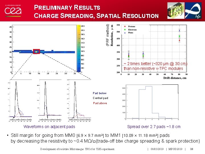
(PRF method) PRELIMINARY RESULTS CHARGE SPREADING, SPATIAL RESOLUTION ~ 2 times better (~320 µm @ 30 cm) than non-resistive v-TPC modules Pad below Central pad Pad above Waveforms on adjacent pads Spread over 2. 7 pads ~1. 8 cm • Still margin for going from MM 0 [6. 9 × 9. 7 mm 2] to MM 1 [10. 09 × 11. 18 mm 2] pads by decreasing the resistivity to ~0. 4 MΩ/□ (trade-off btw charge spreading & spark protection) Development of resistive Micromegas TPCs for T 2 K experiment | 08/05/2019 | MPGD 2019 | 18

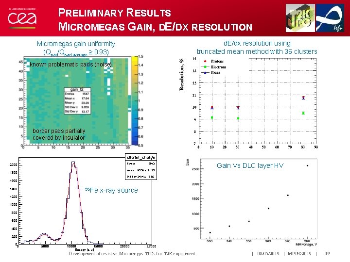
PRELIMINARY RESULTS MICROMEGAS GAIN, DE/DX RESOLUTION d. E/dx resolution using truncated mean method with 36 clusters Micromegas gain uniformity (Qpad/Qpad average ≥ 0. 93) known problematic pads (noise) border pads partially covered by insulator cluster_charge Entries 2000 12913 Mean 9530 ± 21. 25 1800 Gain Vs DLC layer HV Std Dev 2414 ± 15. 03 1600 55 Fe x-ray source 1400 1200 1000 800 600 400 200 0 0 5000 10000 15000 Energy [a. u. ] 20000 25000 Development of resistive Micromegas TPCs for T 2 K experiment | 08/05/2019 | MPGD 2019 | 19

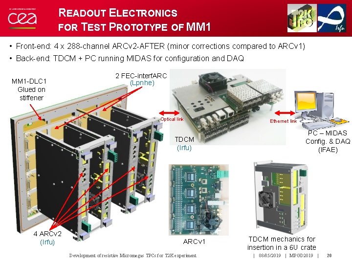
READOUT ELECTRONICS FOR TEST PROTOTYPE OF MM 1 • Front-end: 4 x 288 -channel ARCv 2 -AFTER (minor corrections compared to ARCv 1) • Back-end: TDCM + PC running MIDAS for configuration and DAQ MM 1 -DLC 1 Glued on stiffener 2 FEC-interf. ARC (Lpnhe) Optical link TDCM (Irfu) 4 ARCv 2 (Irfu) ARCv 1 Development of resistive Micromegas TPCs for T 2 K experiment Ethernet link PC – MIDAS Config. & DAQ (IFAE) TDCM mechanics for insertion in a 6 U crate | 08/05/2019 | MPGD 2019 | 20

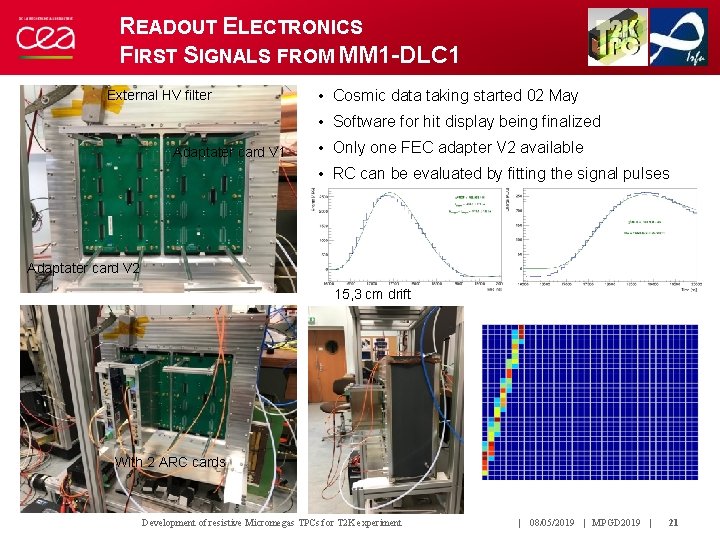
READOUT ELECTRONICS FIRST SIGNALS FROM MM 1 -DLC 1 External HV filter • Cosmic data taking started 02 May • Software for hit display being finalized Adaptater card V 1 • Only one FEC adapter V 2 available • RC can be evaluated by fitting the signal pulses Adaptater card V 2 15, 3 cm drift With 2 ARC cards Development of resistive Micromegas TPCs for T 2 K experiment | 08/05/2019 | MPGD 2019 | 21

CONCLUSIONS &PERSPECTIVES • The tests of a resistive bulk-Micromegas module on CERN/PS-T 9 beam showed a 2 times better spatial resolution while keeping the d. E/d. X capabilities in control (9 -10% with only one module track length) • Analysis is on-going to understand, measure the DLC resistivity non-uniformity • A small prototype of a HA-TPC field cage equipped with a full-size resistive bulk Micromegas module MM 1 will be tested with beam at DESY in June 2019 • The T 2 K / ND 280 near detector upgrade development is on-going (FEC, FC, test bench • The 2 new HA-TPCs design will be soon fixed and production should start in October 2019 for a completion scheduled for march 2021 Development of resistive Micromegas TPCs for T 2 K experiment | 08/05/2019 | MPGD 2019 | 22

THANK YOU Development of resistive Micromegas TPCs for T 2 K experiment | 08/05/2019 | MPGD 2019 | 23

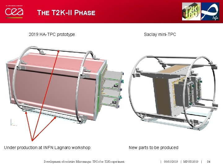
THE T 2 K-II PHASE 2019 HA-TPC prototype Under production at INFN Lagnaro workshop Development of resistive Micromegas TPCs for T 2 K experiment Saclay mini-TPC New parts to be produced | 08/05/2019 | MPGD 2019 | 24

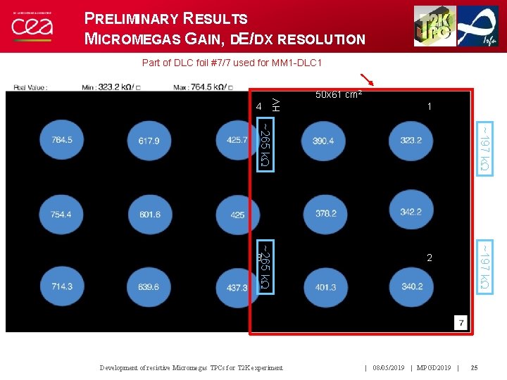
PRELIMINARY RESULTS MICROMEGAS GAIN, DE/DX RESOLUTION 4 4 HV Part of DLC foil #7/7 used for MM 1 -DLC 1 50 x 61 cm 2 1 1 2 ~197 k. W ~265 k. W Development of resistive Micromegas TPCs for T 2 K experiment ~197 k. W ~265 k. W 3 3 2 | 08/05/2019 | MPGD 2019 | 25

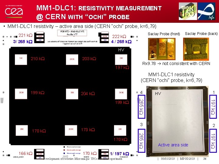
MM 1 -DLC 1: RESISTIVITY MEASUREMENT @ CERN WITH “OCHI” PROBE • MM 1 -DLC 1 resistivity – active area side (CERN “ochi” probe, k=6, 79) 4 221 k. W 3/ 265 k. W Saclay Probe (front) 222 k. W 4 / 265 k. W 1 Saclay Probe (back) HV 210 k. W 203 k. W 197 k. W Rx 9. 78 not consistent with CERN 3 2 MM 1 -DLC 1 resistivity (CERN “ochi” probe, k=6, 79) 4 204 k. W 197 k. W 265 k. W 199 k. W 1 HV HV filter 199 k. W 3 166 k. W 170 k. W 197 k. W 170 k. W 265 k. W 170 k. W 2 173 k. W Active area side 1/ 197 k. W Development of resistive Micromegas TPCs for T 2 K experiment | 08/05/2019 | MPGD 2019 | 26